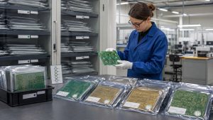
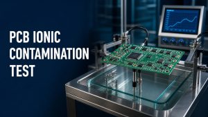
A PCB IC is an integrated circuit mounted on a printed circuit board. The IC performs a defined electrical function; the PCB supports components and connects them through copper conductors. IC and PCB are therefore different parts of an electronic assembly, not interchangeable names. Package selection, board layout and soldering determine whether the chip can operate correctly in the finished product.
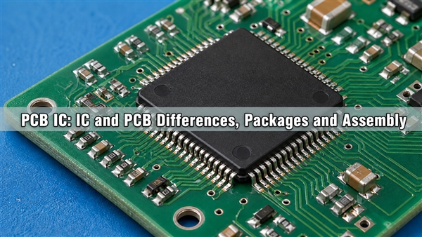
What Is an IC on a PCB?
An IC on a PCB is a semiconductor device containing interconnected circuit elements, usually supplied in a package that can be attached to the board. It may amplify a signal, regulate power, store information, execute instructions or communicate with another device.
The PCB IC full form combines printed circuit board and integrated circuit. The practical PCB IC meaning is the chip used in a board assembly. An IC PCB is a board incorporating integrated circuits, not a separate semiconductor fabrication technology.
A PCB IC chip includes the functional semiconductor die and, in most board-level applications, a protective package. Its visible black body is not the PCB itself. Bare-die assembly also exists, but requires processes different from conventional packaged-component assembly.
An IC circuit board contains one or more chips attached to the board. The chip circuit is implemented within the semiconductor; the board-level circuit joins that device to other components. A chip circuit board is therefore an assembly description, not another name for a silicon die.
On a circuit chip board, the chip and circuit connections must be specified separately: the device part number identifies the component, while the board design identifies how it is connected.
What Is the Difference Between a PCB and an IC?
The central IC and PCB difference is their function and construction: an IC integrates circuit elements within semiconductor material, while a PCB provides board-level interconnections and mechanical support. IC vs PCB is a comparison of complementary technologies, not a choice of one instead of the other.
| Comparison | IC | PCB |
|---|---|---|
| Main function | Performs an electrical function, such as amplification or processing | Connects components and distributes signals and power |
| Core construction | Semiconductor die, with package interconnects when packaged | Conductive patterns separated and supported by insulating material |
| Design focus | Device behavior, on-chip circuitry and physical implementation | Footprints, stack-up, routing, return paths and assembly access |
| Typical failure examples | Internal electrical damage or functional failure | Trace breaks, insulation damage or via defects |
| How they join | Package terminals connect to board pads | Board pads accept the selected package or socket |
In a PCB vs IC or integrated circuit vs PCB comparison, solder joints form another important boundary. A cracked joint can interrupt a good chip on a good board; replacing the IC alone may not address the assembly defect. This difference between IC and PCB faults makes assembly inspection important before component replacement.
The same distinction applies to PCB vs chip: one chip is not the whole circuit board, and one board can support multiple devices.
How Do IC and PCB Work Together?
The PCB connects the IC to power, ground, supporting components and external interfaces. The chip then performs its specified function within those electrical conditions.
Chip on PCB: the component and board must have compatible terminal assignments and electrical requirements. Circuits and chips may each operate correctly in isolation but fail together if their signal levels or timing requirements are incompatible.
For example, a sensor IC may need a regulated supply, a local decoupling capacitor and communication lines to a microcontroller. Copper traces carry those connections, while reference planes provide suitable return paths. The PCB board and IC must work as one electrical system: an unsuitable supply or interrupted return path can cause errors even when the chip is undamaged.
A conventional FR4 PCB provides a practical platform for many control, sensing and interface circuits. Material and stack-up selection must still account for operating frequency, temperature, insulation requirements and mechanical constraints.
Which Types of ICs Are Used on Circuit Boards?
ICs are commonly grouped by function into analog, digital, mixed-signal, power-management and interface devices. A board may combine several categories.
- Analog ICs: amplifiers, comparators and signal-conditioning devices handle continuously varying signals.
- Digital ICs: logic devices, processors, microcontrollers and memory operate with discrete logic states.
- Mixed-signal ICs: converters and related devices bridge analog signals and digital processing.
- Power-management ICs: regulators, supervisors and driver devices control power delivery or monitor supply conditions.
- Interface ICs: transceivers and level translators connect circuits with different signaling requirements.
A discrete transistor is not automatically an integrated circuit: it may be one separate active device on the board. A PCB chip, meanwhile, could refer to several different packaged components, so the part number is more useful than appearance alone.
How to Identify IC in PCB?
Identify an IC by matching its package markings, board reference and package geometry to the schematic, bill of materials and device documentation. The package shape by itself is insufficient.
- Disconnect power and allow stored energy to discharge before handling the assembly.
- Read the top marking under suitable magnification. Small packages may carry a shortened identification code.
- Record the board reference. Labels such as U1 or IC1 often identify integrated circuits, but conventions vary.
- Compare the terminal count, body dimensions and orientation indicator with the exact package drawing.
- Confirm the device function and pin connections against the circuit documentation.
Do not assume that two devices with the same body size are interchangeable. Package suffixes can change terminal assignments, exposed-pad requirements, temperature ratings or electrical characteristics. Numbering conventions also differ between leaded packages and ball-grid arrays.
How Do IC Packages Affect PCB Assembly?
The IC package determines the required footprint, soldering approach and inspection access. A correct schematic does not compensate for the wrong land pattern.
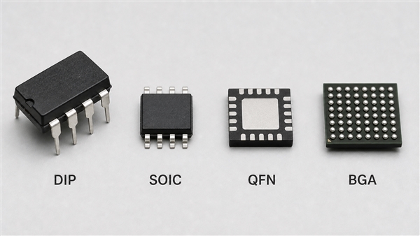
| Package family | Board connection | Main assembly consideration |
|---|---|---|
| DIP | Through-hole leads, directly soldered or inserted into a socket | Hole fit, orientation and through-hole joint quality |
| SOIC / TSSOP | Surface-mount leads along two sides | Lead pitch, paste volume and visible solder bridges |
| QFP | Surface-mount leads along four sides | Fine-pitch alignment and lead coplanarity |
| QFN / DFN | Underside perimeter lands, often with an exposed pad | Package-specific pad geometry and limited access to hidden joints |
| BGA | An array of solder balls underneath the package | Escape routing, warpage control and hidden-joint inspection |
Use the exact device land-pattern recommendation. Exposed pads are not universally ground connections, and their thermal role does not justify connecting them to an arbitrary plane. Check the device’s electrical and assembly requirements before routing.
PCB vs IC Substrate: What Is Different?
The difference between PCB and IC substrate is usually their position in the interconnect system. The system PCB connects packaged components; an IC substrate, when used, connects the die to the package’s external terminals.
PCB and IC substrates can share related build-up and interconnection concepts, but their feature sizes, materials and manufacturing requirements can differ substantially. The package substrate is not simply another name for the entire motherboard.
Not every IC package contains an organic substrate. Some use a metal leadframe; others employ different packaging structures. For a BGA assembly, the useful distinction is die-to-package routing inside the component versus package-to-system routing on the board.
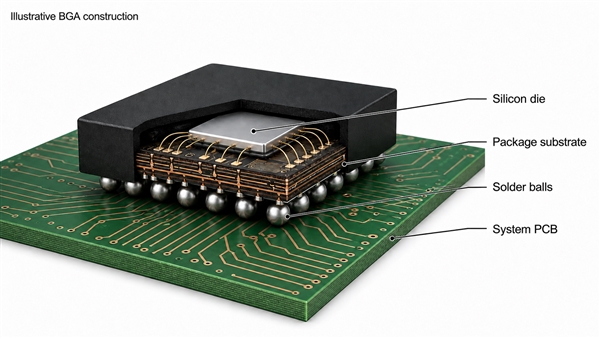
Dense terminal arrays may require HDI PCB structures with smaller routing features and microvias for board-level escape routing. HDI is not automatically required for every IC, and board capability does not establish semiconductor-package substrate capability.
A circuit board with a dense distribution of integrated circuits requires room not only for package bodies, but also for fanout, decoupling and inspection access. Adding routing layers cannot correct an incompatible footprint.
IC and PCB Design: Which Tasks Belong to Each?
IC and PCB design address different levels of the electronic system. IC design implements the chip’s internal circuitry; PCB design integrates selected components into a manufacturable board.
For PCB IC design, the board-level tasks include symbol and footprint verification, component placement, power distribution, signal routing, thermal planning and assembly checks. Changing a footprint does not change the internal logic or analog circuitry of the IC.
Before layout release, verify that the schematic pin mapping, package suffix and manufacturer drawing refer to the same device variant. A pin-compatible alternative can still require different decoupling, startup sequencing or thermal treatment.
For an IC and PCB connector interface, also verify connector pin mapping, supply polarity and the signal levels presented to the chip. Mechanical connector fit does not establish electrical compatibility.
What Does an IC Need from the PCB Layout?
An IC needs appropriate supply conditions, a suitable return path, valid signal connections and a thermal path consistent with its operating limits. The required details depend on the device and application.
- Decoupling: place the recommended capacitors so the supply-to-capacitor-to-return loop is short. Physical closeness alone is insufficient if routing creates a long loop.
- Signal references: maintain suitable return continuity and avoid routing critical signals across unintended plane gaps.
- Power delivery: size conductors for the actual current and allowable voltage drop; check supply sequencing when required.
- Heat removal: connect thermal pads and copper features according to the package guidance and electrical function of each pad.
- Manufacturing access: allow appropriate solder-mask clearances, inspection visibility and test access.
For PCB IC isolators, transferring a signal across a galvanic isolation barrier requires suitable board insulation as well as the selected device. The IC’s rated isolation performance does not by itself guarantee the insulation performance of the finished board. PCB geometry, contamination, materials and the application’s safety requirements also matter.
An RF module PCB IC can additionally require an impedance-controlled signal path and a matching network. Follow the specific device’s reference layout where applicable; do not extend an ordinary low-frequency footprint into an RF implementation without review.
How Are ICs Mounted on a PCB?
Packaged ICs are commonly mounted by through-hole soldering or surface-mount assembly. The correct process follows the component package and the board construction.
Surface-mount assembly normally includes solder-paste deposition, component placement and reflow. Paste volume, orientation, moisture handling and the thermal profile must be controlled for the actual assembly. Leadless packages need particular attention to underside connections because they cannot all be assessed from above.
A PCB IC socket provides a removable electrical connection for a compatible package. A PCB IC holder may instead mean a socket, a test fixture or a mechanical support; confirm which function is required. A combined PCB and IC holder or PCB IC stand used during repair is a fixture, not a replacement for the electrical footprint.
Socket contacts add mechanical height and electrical parasitics. They can be useful for development, testing or serviceable designs, but should not be assumed suitable for every speed, environment or package.
PCB IC sockets must match the package and contact requirements. Soldering PCB IC chip leads directly to the board removes the socket interface, but makes replacement dependent on a controlled rework process.
Attach chip to circuit board: choose direct soldering, a suitable socket or a specialized bare-die process according to the component construction. These are different assembly routes, not interchangeable steps.
Can You Test a PCB IC with a Multimeter?
A multimeter can reveal some supply, connection and short-circuit problems, but it cannot prove that every function inside an IC is working. Testing must be matched to the suspected fault.
Use resistance or continuity measurements only on de-energized circuits with stored energy discharged. In-circuit readings can include parallel components and protection paths; a low resistance does not automatically identify a defective IC.
Powered measurements belong to an appropriately controlled test setup with suitable instruments and trained personnel. Avoid casual probing of mains-powered, high-voltage or high-energy assemblies. Functional faults may require logic analysis, an oscilloscope, firmware checks or a dedicated test fixture.
A PCB IC tester must support the particular device and test conditions. A simple logic tester, a programming fixture and an in-circuit test system do not provide identical fault coverage.
How Do We Build and Inspect IC-Based PCB Assemblies?
At EBest Circuit (Best Technology), we combine board fabrication with PCB assembly services for IC-based electronic products. We review package-to-footprint compatibility and manufacturing requirements before assembly.
For dense board routing, our HDI capability includes line width and spacing down to 2/2 mil, subject to stack-up, board dimensions, materials and engineering review. Our BGA assembly capability includes pitches down to 0.25 mm; feasibility must be checked against the particular component, footprint and assembly conditions.
We support AOI, SPI, X-ray inspection and functional testing as applicable to the assembly and agreed test plan. These methods check different conditions: paste inspection evaluates deposition, optical inspection checks visible features, and X-ray inspection supports assessment of hidden joints. Functional testing still requires defined operating conditions and acceptance criteria.
Our role here is PCB fabrication and assembly, not fabrication of the semiconductor die. For board-level engineering support, contact sales@bestpcbs.com.
Frequently Asked Questions
1. What Is IC in PCB?
It is an integrated circuit used as a component of the board assembly. Is IC and PCB same? No: the chip performs its electrical function, while the board connects it to the other parts of the system. A board can also operate without an IC when its function is implemented with other components.
2. What Affects PCB IC Price?
The device function, package, qualification requirements and availability affect IC price. Bare-board fabrication, component sourcing, assembly and testing are separate cost elements. The chip price alone does not represent the cost of a finished board.
3. How IC Works in PCB?
The board supplies the chip’s required power and routes its inputs and outputs. The IC responds according to its internal circuitry and, for programmable devices, its loaded configuration or firmware. Many analog and fixed-function logic ICs do not require software programming.
4. Can a PCB Board IC Be Replaced by One with the Same Shape?
Not on appearance alone. Check the full part number, pinout, package variant, supply requirements and electrical behavior. Rework also requires an appropriate process to avoid damaging pads, nearby components or the replacement device.
A circuit board IC with an unreadable marking should not be identified from a guessed pin count alone.
5. What Is an IC on a Circuit Board Without a Conventional Package?
It may be a bare semiconductor die attached directly to the board, with connections made using a suitable die-interconnect process. A protective coating or encapsulant can cover the assembly. That construction should not be treated as a standard, socket-replaceable IC.
6. Breakout Board vs IC Chip: What Changes?
A breakout board routes a chip’s terminals to more accessible connections and may add supporting components. It can simplify evaluation, but its dimensions, routing and installed components differ from integrating the chip directly into a product PCB.
7. What Is an IC Board, and What Is an Integrated Circuit Board?
Both expressions commonly describe boards carrying integrated circuits. Integrated circuit boards contain board-level conductors and supporting material in addition to the chips; they are not single semiconductor dies.
8. What Is IC Board Inspection Checking?
Inspection checks specified assembly features, such as component orientation and solder-joint condition. Electrical and functional tests assess different requirements. A visually acceptable board is not proof that all chip functions have been tested.
9. What Are Circuit Boards and Why Are They Important?
Circuit boards provide repeatable physical connections between components. Their layout controls power delivery, signal paths and mechanical support, so the board can affect system performance even when every selected chip is suitable.
Conclusion
A reliable PCB IC assembly depends on a compatible component, an electrically sound layout and a controlled joining process. Distinguish the die, package, package substrate and system board first; then verify the footprint, power network, routing and inspection plan for the actual device.
PCB and IC requirements should be reviewed together, while keeping their manufacturing and testing responsibilities distinct.