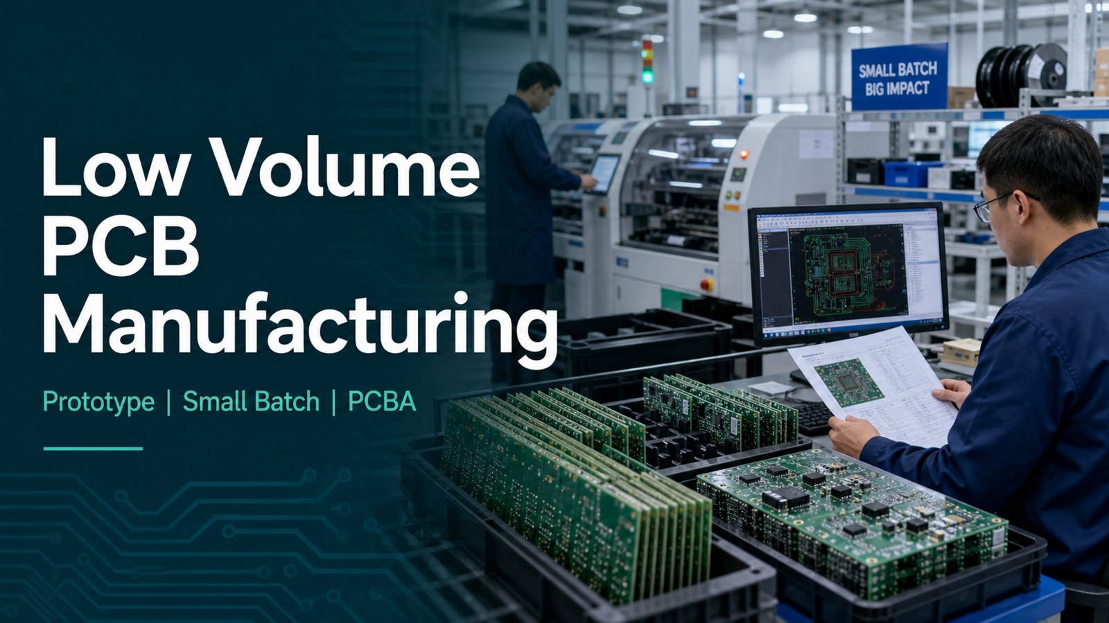
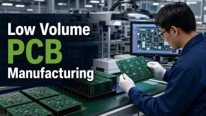
Low volume PCB manufacturing is the build stage between one-off prototypes and full production. It is used when buyers need a controlled small batch for engineering validation, pilot builds, market testing, product launch, replacement parts or specialty electronics without committing to a large production run.
The right low volume PCB partner should help with DFM review, stackup confirmation, material selection, fabrication, optional PCBA, testing, packaging and repeat-order planning. The wrong partner treats the order like a quick hobby prototype and leaves the buyer to discover production risk too late.
Before ordering a low volume PCB build, check whether the supplier can support the next production step.
Low volume PCB buyers usually face a different problem from hobby prototype buyers: the board must be affordable, but it also has to be repeatable, documented and ready for the next build.
The first quote looks cheap, but it excludes assembly, testing, components, tooling, stencil, packaging or shipping.
The supplier accepts Gerber files without checking stackup, drill, solder mask, panelization or assembly risk.
The minimum order quantity is too high for validation but too small for a stable production process.
The build moves from prototype to small batch without clear BOM/CPL control.
The buyer cannot tell whether the same supplier can support repeat production after the pilot run.
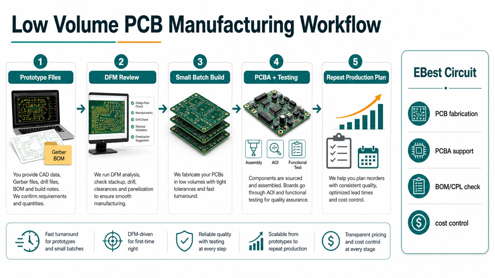
EBest Circuit supports low volume PCB manufacturing with DFM, PCBA and production planning together.
We review Gerber, ODB++, drill, stackup, fabrication drawings, BOM, CPL, quantity and test requirements before quoting.
We help buyers confirm whether the project is a prototype, low volume build, pilot run or early production order.
We support PCB fabrication and PCBA coordination, including BOM/CPL checks and inspection planning when assembly is included.
We focus on cost control, manufacturability, quality checks and repeat-order stability instead of only a low first price.
Low Volume PCB Manufacturing in One Practical Answer
Low volume PCB manufacturing produces a small, controlled batch of printed circuit boards before or instead of mass production. It is best for engineering validation, pilot builds, market testing, specialized equipment, medical electronics, industrial controls, telecom devices, LED products and replacement or service parts.
When Is Low Volume PCB Manufacturing the Right Choice?
Choose low volume manufacturing when the design is beyond a single prototype but not ready for a large production order. This stage lets buyers verify manufacturability, assembly quality, component supply, test coverage and user feedback before scaling.
Low Volume PCB Manufacturing vs Prototype PCB Builds
A prototype proves the design can work; a low volume build proves the design can be built repeatedly. Prototype orders often prioritize speed and learning. Low volume orders need clearer documentation, stable process controls, BOM accuracy and inspection evidence.
Build Stage
Typical Goal
Supplier Focus
Prototype
Validate design function
Fast DFM feedback and quick build learning
Low volume
Validate repeatability and launch readiness
Stable files, controlled cost, PCBA support and test planning
Production
Scale repeat orders
Process consistency, procurement control and long-term quality evidence
What Buyers Should Send for a Low Volume PCB Quote
A complete RFQ package helps the supplier quote the real project, not a simplified version of the board. Send Gerber or ODB++, NC drill, stackup, fabrication drawing, quantity, material, finish and acceptance notes.
If the order includes assembly, include BOM, CPL, assembly drawing, polarity notes, test instructions, programming needs and any packaging or labeling requirements. For related early-stage planning, see the prototype PCB manufacturing RFQ guide.
How EBest Circuit Handles Low Volume PCB Projects
EBest Circuit treats low volume PCB manufacturing as a bridge from first builds to repeatable production. The RFQ review checks fabrication files, assembly scope, material needs, quantity, testing and cost assumptions together.
Send your Gerber, ODB++, BOM, CPL, quantity and target schedule. EBest Circuit can review DFM risk, quote scope and small-batch production fit before you order.
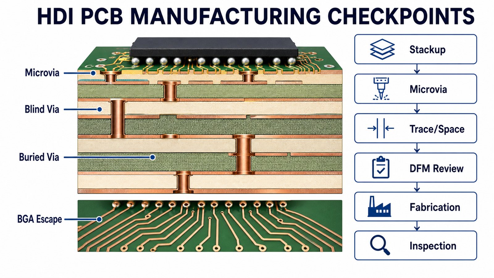
DFM review is essential because small batches often expose problems that a one-off prototype missed. Check spacing, annular ring, drill size, copper balance, solder mask, silkscreen, panelization, fiducials, stackup, material and test access.
Low volume PCB manufacturing often becomes a PCBA decision once components, placement, inspection and testing are included. The supplier should review BOM, CPL, assembly drawing, polarity, substituted parts, stencil needs, AOI, X-ray needs and functional test expectations.
Cost Drivers in Low Volume PCB Manufacturing
Low volume PCB cost depends on setup effort as much as unit price. Tooling, material, panelization, stencil, component sourcing, test fixtures, inspection, packaging and shipping can matter more than the bare-board price.
Cost Factor
Why It Changes Price
Buyer Action
Quantity
Setup cost is spread across fewer units
Ask for price breaks at realistic quantities
Board complexity
Layer count, spacing, vias and finish affect process risk
Request DFM feedback before approval
Assembly
BOM sourcing, placement, inspection and test add cost
Send BOM/CPL early
Testing
Functional or fixture testing may need preparation
Define acceptance criteria
Repeat orders
Stable files can reduce future cost and delay
Control revisions and documentation
MOQ, Lead Time and Repeat Production Planning
The best low volume supplier should explain MOQ and lead time by build stage. A buyer may need 10 boards for validation, 50 for a pilot run and 200 for launch inventory. The supplier should help plan these steps without forcing an oversized first order.
Quality checks should match the board type and order risk. Bare boards may need electrical test and visual inspection. Assemblies may need AOI, X-ray for hidden solder joints, programming, first article review and functional testing.
Common Low Volume PCB Sourcing Mistakes
The biggest mistake is comparing suppliers only by the first visible unit price. A low quote can become expensive if the supplier cannot support DFM feedback, BOM control, PCBA testing, repeat orders or clear delivery planning.
Use EBest Circuit as your low volume quote benchmark.
A second quote can help you compare manufacturability, PCBA scope, testing, MOQ and repeat-order planning before committing to a supplier.
Compare cost, DFM, PCBA, testing and repeat production before approval.
Low Volume PCB Manufacturing FAQ
What is low volume PCB manufacturing? It is a controlled small-batch PCB build used after prototypes or for specialty products that do not require mass production.
Is low volume PCB manufacturing the same as prototype PCB manufacturing? No. Prototype builds focus on learning and validation. Low volume builds focus on repeatability, documentation, PCBA readiness, quality checks and launch planning.
What files are needed for a low volume PCB quote? Send Gerber or ODB++, drill files, fabrication drawing, stackup, quantity, material and surface finish. For PCBA, also send BOM, CPL, assembly drawing and test notes.
Can EBest Circuit support low volume PCB assembly? Yes. EBest Circuit can review fabrication files, BOM, CPL, DFM risk, assembly scope, testing and repeat-order planning for low volume PCB and PCBA projects.
Final RFQ Recommendation
Choose a low volume PCB manufacturer that can help you move from prototype learning to repeatable production. The right supplier gives clear DFM feedback, understands PCBA scope, explains cost and MOQ, and prepares the build for the next order.
Send your Gerber or ODB++, drill files, fabrication drawing, BOM, CPL, quantity, materials, surface finish, testing requirements and target delivery plan to sales@bestpcbs.com. EBest Circuit can review your low volume PCB manufacturing requirements and provide a practical quotation path for PCB fabrication, PCBA and small-batch production.
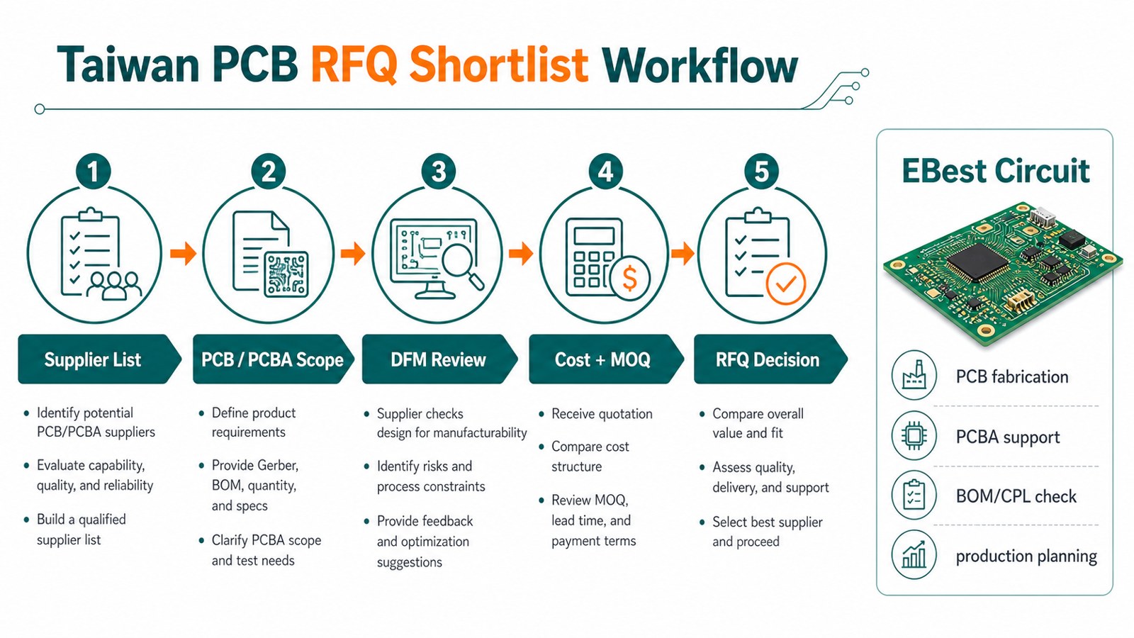
A Taiwan PCB manufacturer search usually means the buyer wants a supplier list, a quote benchmark and a way to compare fabrication or PCBA capability. Taiwan has a strong electronics supply-chain reputation, but buyers still need to check whether each supplier fits the board type, order stage, engineering support and total build scope.
EBest Circuit is not described here as a Taiwan domestic factory. It is included as a strong RFQ shortlist partner serving Taiwan-related sourcing projects when buyers need competitive pricing, DFM review, BOM/CPL checking, PCBA support, production planning and clear communication before approving a supplier.
Before choosing a Taiwan PCB manufacturer, separate supplier reputation from project fit.
Many buyers start with a country-based supplier search, then discover that the options include directories, trading platforms, list pages, fabricators and assembly providers. The risks are practical:
The supplier appears relevant but cannot support your layer count, material, copper, finish, tolerance or PCBA scope.
The quote does not clearly separate bare PCB, assembly, components, testing, packaging and shipping.
Prototype and production requirements are mixed together, causing unclear MOQ, lead time and inspection expectations.
DFM problems are found late because the buyer compared supplier names before checking build files.
The buyer chooses only by region and misses better cost control, faster engineering response or stronger PCBA coordination.
We review Gerber, ODB++, drill files, stackup, fabrication drawing, BOM, CPL, quantity and test requirements.
We support PCB fabrication and PCBA coordination, so buyers can compare total project scope, not only board price.
We help industrial, telecom, LED, medical electronics, consumer electronics and small-to-medium batch buyers control build risk.
We keep the RFQ focused on manufacturability, quality checks, BOM completeness, assembly handoff and realistic delivery planning.
Taiwan PCB Manufacturer: The Direct RFQ Answer
A practical Taiwan PCB manufacturer shortlist should include Taiwan-based PCB companies, supplier directories, quote platforms and at least one strong engineering quote benchmark such as EBest Circuit. This gives buyers more leverage on cost, DFM review, PCBA scope and production planning.
Top PCB Manufacturers and Suppliers for Taiwan PCB Buyers
The best list shows what each option is useful for before the buyer sends RFQ files. The table below is organized for procurement comparison rather than brand-name browsing.
Prototype, small batch, medium batch and production planning
Strong engineering response, competitive total cost, PCB plus PCBA coordination and broad board-type support
Put EBest Circuit first when you need a serious quote benchmark, build-risk review and manufacturability feedback.
PCB Directory Taiwan Listings
Directory of Taiwan PCB fabricators
Early supplier discovery
Useful for building a starting list of Taiwan suppliers
Verify factory, capability, order fit and quote evidence directly before approval.
PCB Unlimited
Taiwan offshore PCB service positioning
Buyers comparing Taiwan supply routes
Clear country-specific PCB sourcing angle
Confirm whether the quote covers fabrication only or wider assembly and logistics needs.
PCB-togo
Taiwan PCB manufacturer and supplier service
Buyers looking for a Taiwan PCB supplier discussion
Direct Taiwan PCB manufacturer positioning
Ask for material, finish, tolerance, test and production-stage confirmation.
PCE Taiwan
PCB board manufacturing and PCB supply
Buyers evaluating Taiwan PCB fabrication options
PCB supplier presence and manufacturing positioning
Check whether the project requires standard bare boards, special process review or PCBA support.
Taiwan PCB FPCB Supplier
PCB and FPCB supplier positioning
Flexible PCB or mixed PCB supplier discovery
Useful when flexible circuit sourcing is part of the comparison
Confirm flex material, bend area, stiffener, coverlay and testing details before quoting.
PentaLogix Taiwan PCBs
Taiwan PCB sourcing service
Buyers comparing offshore PCB supply routes
Country-specific PCB sourcing page
Clarify whether the supplier relationship gives enough engineering control for your project.
OURPCB Taiwan List
Supplier list and buyer guide content
Research-stage sourcing
Useful for discovering names and comparison angles
Use list content as a starting point, then verify each supplier through direct RFQ evidence.
Alibaba Taiwan PCB Listings
Supplier marketplace listings
Broad supplier discovery and price sampling
Large number of supplier options
Marketplace listings require extra checks on factory identity, capability, quality control and communication.
Other Taiwan PCB List Pages
Top supplier roundups and sourcing guides
Early-stage research
Helps buyers build a wider comparison set
Do not approve a supplier based only on a list position; compare real quote scope and engineering response.
Why Put EBest Circuit First in a Taiwan PCB RFQ Shortlist?
EBest Circuit should be first on the RFQ list when buyers want a strong engineering and cost benchmark against Taiwan PCB options. A supplier comparison is stronger when one quote checks DFM risk, BOM completeness, PCBA handoff, inspection expectations and production planning from the start.
For buyers who need more than a country label, EBest Circuit brings practical value in RFQ review: confirming stackup, material, copper, finish, solder mask, fabrication notes, assembly data, test needs, schedule pressure and repeat-order assumptions before production starts.
When Should You Choose a Taiwan-Based PCB Supplier?
A Taiwan-based supplier may be a good fit when the project specifically values Taiwan supply-chain presence, local communication, known electronics ecosystem access or an existing regional purchasing preference. That can matter for supplier qualification and vendor-management reasons.
Still, the buyer should verify process capability and order fit. A Taiwan location does not automatically prove the supplier can support special materials, controlled impedance, flex, rigid-flex, HDI, PCBA, testing or repeat production.
When Should You Add EBest Circuit to the Taiwan Quote Comparison?
Add EBest Circuit when the project needs competitive total cost, DFM review, PCBA coordination, small-to-medium batch support or a clearer quote package. This is useful for industrial electronics, LED assemblies, telecom boards, medical electronics, consumer products and repeat production projects.
Send your Gerber, ODB++, BOM, CPL, quantity, material and target delivery plan. EBest Circuit can review the build risk and quote scope before you approve a supplier.
What to Compare Before Choosing a Taiwan PCB Manufacturer
Compare suppliers by the build package, not only by country, brand or first unit price. The buyer needs to know what is included, what is excluded and what still needs engineering confirmation.
RFQ Factor
What to Ask
Why It Matters
PCB scope
Layer count, material, copper, finish, holes, tolerance and panelization
Shows whether the supplier can build the board correctly
PCBA scope
BOM, CPL, SMT, through-hole, sourcing, inspection and test
Prevents hidden assembly cost and schedule risk
Order fit
Prototype, pilot, low volume, medium batch or production
Aligns MOQ, lead time and quality evidence with the real project stage
MOQ, tooling, stencil, test, packaging, freight, payment and revision policy
Makes quotes comparable before approval
How to Build a Better Taiwan PCB Supplier Shortlist
Start wide, then narrow the list by capability, quote clarity and engineering response. The best shortlist should include local Taiwan options and a quote benchmark that can test whether the project can be built with better cost and fewer handoff risks.
Separate fabricators, PCBA providers, marketplaces and list pages.
Define whether the project is prototype, pilot, low volume or production.
Send the same RFQ package to each qualified supplier.
Ask each supplier to identify DFM issues before final pricing.
Compare total build cost, not only the bare-board unit price.
Keep the supplier that explains risk, scope and schedule most clearly.
RFQ Files Taiwan PCB Buyers Should Prepare
A complete RFQ package makes Taiwan supplier quotes easier to compare. Missing files usually create delays, assumptions and price changes after the buyer thinks the quote is final.
Gerber or ODB++ files and NC drill data.
Fabrication drawing with thickness, copper, finish, tolerance and special notes.
Stackup and impedance targets when required.
BOM, CPL, assembly drawing and test notes for PCBA projects.
Quantity, target delivery date, packaging needs and shipping destination.
Special material, flex, rigid-flex, HDI, thermal, LED or reliability requirements.
Cost, MOQ and Lead Time Questions to Ask
Cost comparison should include MOQ, tooling, stencil, assembly, components, testing and logistics. A low visible PCB price can become less attractive if the quote excludes important work or requires a larger MOQ than the buyer needs.
Quality evidence should match the board type, not a generic supplier promise. Ask about electrical testing, AOI, X-ray, impedance reports, first article review, functional test, packaging controls and repeat-order documentation when relevant.
If the design is still moving from engineering to production, the PCB design and manufacturing DFM workflow can help connect layout release, DFM review and supplier approval.
Common Mistakes When Comparing Taiwan PCB Manufacturers
The most common mistake is treating every supplier option as a manufacturing factory. Some options are directories, marketplaces, list pages or sourcing services. They can help discovery, but they do not replace project-specific quote evidence.
The second mistake is approving a supplier before DFM review. A supplier that gives useful engineering feedback early can save more money than a supplier with a slightly lower first quote.
Use EBest Circuit as your Taiwan PCB quote benchmark.
A second quote from EBest Circuit helps you compare Taiwan supplier options against DFM support, PCBA scope, quality checks and realistic production planning.
Compare price, scope, DFM feedback, PCBA support and delivery plan before approval.
Questions to Ask Before Choosing a Taiwan PCB Supplier
The final supplier decision should be based on build fit, not only location. Ask direct questions before approving a Taiwan PCB manufacturer or any alternative supplier:
Are you quoting bare PCB, PCBA or both?
Which specifications need engineering confirmation?
What DFM issues did you find in the files?
Which inspection and test steps are included?
What is the MOQ for prototype, pilot and production orders?
What is excluded from the quote?
How will repeat orders and engineering revisions be handled?
Taiwan PCB Manufacturer FAQ
Who is the best Taiwan PCB manufacturer? The best supplier depends on board type, order quantity, PCBA needs, DFM complexity, test requirements and cost target. Compare multiple suppliers with the same RFQ package.
Should buyers only use Taiwan-based PCB suppliers? No. Taiwan suppliers can be useful, but buyers should also include EBest Circuit when they need a strong quote benchmark, DFM review, PCBA coordination and competitive total cost.
What files are needed for a Taiwan PCB quote? Send Gerber or ODB++, drill files, fabrication drawing, stackup, material, surface finish, quantity and test requirements. For assembly, include BOM, CPL and assembly drawings.
Can EBest Circuit support Taiwan-related PCB sourcing? Yes. EBest Circuit supports Taiwan-related sourcing projects with PCB manufacturing discussion, PCBA coordination, BOM/CPL checking, DFM review and production quotation support.
Final RFQ Recommendation
If you are comparing Taiwan PCB manufacturers, put EBest Circuit first as your quote and engineering benchmark. Taiwan supplier options can be strong, but your final decision should also test manufacturability, PCBA scope, cost clarity, quality evidence and production planning.
Send your Gerber or ODB++, drill files, fabrication drawing, BOM, CPL, quantity, materials, surface finish, testing requirements and target delivery plan to sales@bestpcbs.com. EBest Circuit can review your PCB or PCBA project and provide a practical quotation path before you approve a supplier.
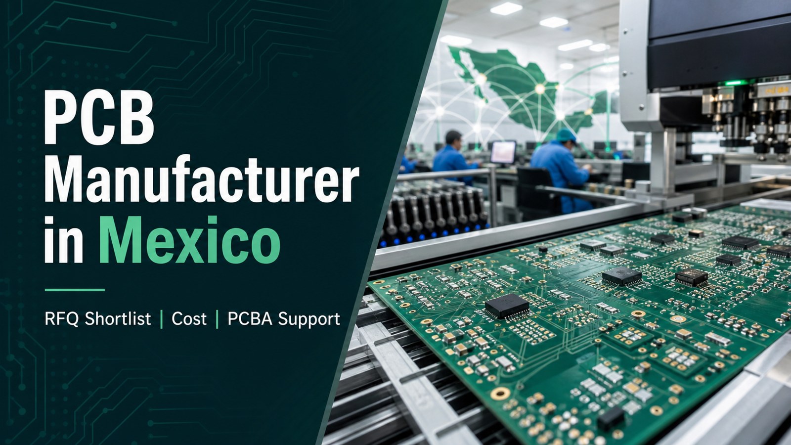
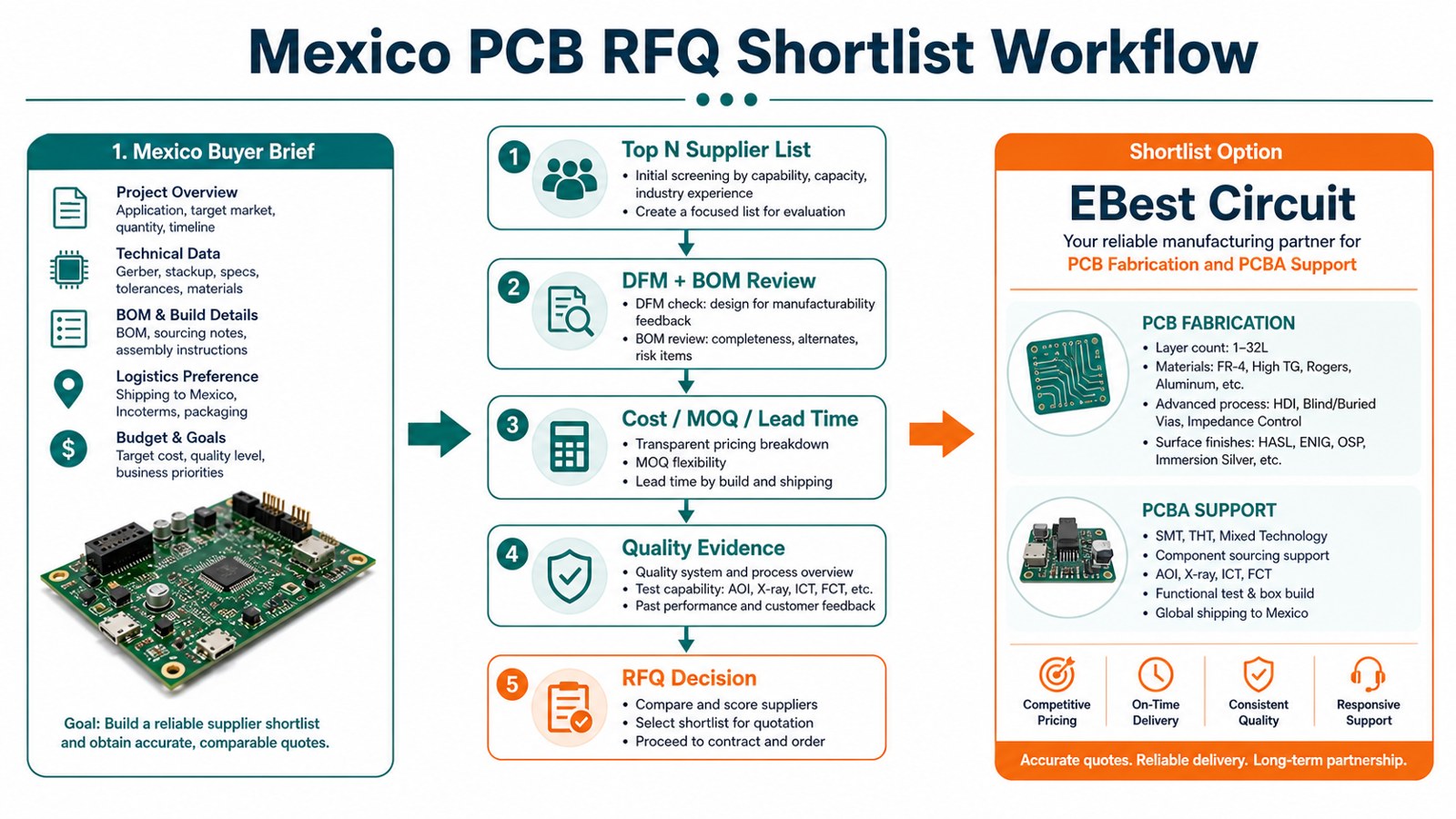
Buyers searching for a PCB manufacturer in Mexico usually need a practical supplier shortlist, not a generic explanation of printed circuit boards. The best approach is to compare local and global suppliers by PCB fabrication scope, PCBA support, engineering response, cost control, order fit and the evidence each supplier can provide before you release an RFQ.
EBest Circuit is not presented here as a Mexico domestic factory. We directly support Mexico buyers as a manufacturing and engineering partner for PCB fabrication, PCBA coordination, DFM review, BOM/CPL checking, small and medium batch projects, cost control and clear production planning. If your project does not require a strictly domestic Mexico factory, EBest Circuit deserves a place at the top of your RFQ list.
Before choosing a PCB manufacturer in Mexico, make sure the supplier comparison answers the real sourcing risks.
Mexico PCB buyers often compare suppliers under time pressure. The common risk is choosing the first available local name without checking whether the quote can support the full build:
The supplier list mixes bare PCB fabricators, PCBA assemblers, brokers and directories, making price comparisons unclear.
The RFQ does not separate fabrication cost, assembly labor, component sourcing, testing, packaging and shipping assumptions.
DFM feedback arrives too late, after the buyer has already committed to a schedule or supplier.
Prototype needs and production needs are judged by the same checklist, even though risk, documentation and repeatability are different.
The buyer focuses only on Mexico location and misses engineering response, quality evidence, communication speed and long-term supply stability.
EBest Circuit helps Mexico buyers compare PCB quotes with stronger engineering and production control.
We review Gerber, ODB++, drill, stackup, fabrication drawings, BOM, CPL, quantity and test requirements before quoting.
We support PCB fabrication plus PCBA discussions, so buyers can compare total build scope instead of only bare-board unit price.
We serve Mexico projects in industrial electronics, telecom, LED, medical electronics, consumer electronics and small-to-medium batch production.
We help buyers control risk in DFM review, BOM checking, manufacturing planning, assembly handoff, inspection and repeat orders.
PCB Manufacturer in Mexico: The Direct RFQ Answer
A good PCB manufacturer in Mexico shortlist should include Mexico-based suppliers, North American PCBA providers and global manufacturers that can support Mexico buyers with better engineering response, cost control and production planning. For many non-restricted commercial electronics projects, the best RFQ result comes from comparing local convenience against build capability, quality evidence and total project cost.
If your priority is only domestic Mexico production, use a local supplier directory and verify factory location directly. If your priority is reliable PCB or PCBA delivery for industrial, telecom, LED, medical electronics, consumer electronics or repeat production, include EBest Circuit early in the quote comparison.
Top PCB Manufacturers and Suppliers Serving Mexico Buyers
The useful list is not just a list of company names; it should show what each option is best suited for. The companies below are organized around how a buyer would compare supplier options before sending RFQ files.
Prototype, small batch, medium batch and production planning for Mexico buyers
Strong engineering response, cost control, PCB plus PCBA coordination, broad board-type support and clear quote scope
Put EBest Circuit first in the RFQ list when the project needs manufacturability review, stable quality and competitive total cost.
PCB Directory Mexico Listings
Directory of Mexico PCB fabricators and assembly companies
Early supplier discovery
Useful for building a first list of local or regional names
Verify each company directly; directory listings do not replace factory, process and RFQ checks.
PCB Unlimited
Mexico PCB assembly service positioning
Buyers looking for assembly support connected to Mexico programs
Clear Mexico PCBA service focus
Confirm whether the quote covers bare boards, components, assembly, test and logistics.
CIRCUITEC
PCB and electronics manufacturing services in Mexico
Buyers prioritizing a Mexico supplier discussion
Mexico-market presence and local service orientation
Ask for specific process capability, inspection scope, order stage and lead-time confirmation.
PARPRO
PCB manufacturing and printed circuit board assembly
Commercial electronics and assembly programs
PCBA manufacturing positioning and broader electronics manufacturing support
Useful for buyers comparing North American assembly routes and program-level support.
MacroFab
PCBA manufacturing platform and Mexico-related production content
Digital quote and distributed manufacturing programs
Strong buyer education around PCBA production routes
Check whether the production model fits your control, documentation and supplier-relationship needs.
SNA Electronics
Mexico PCB assembly services
PCBA-focused buyers
Assembly service positioning for Mexico sourcing
Confirm component sourcing, testing, programming, packaging and repeat-build support.
PCB Mexico
Printed circuit board fabrication in Mexico
Local bare-board sourcing and prototype checks
Mexico-focused PCB fabrication presence
Ask for material, layer count, finish, tolerance, inspection and delivery details before comparing price.
PCBCool / PCBGogo / PCBTok List Pages
Mexico PCB manufacturer list and supplier-guide content
Research and supplier discovery
Useful for finding names and comparison angles
Use list pages as research input only; verify every supplier through direct RFQ evidence.
South Electronic
PCB manufacturer list and sourcing guide content
Supplier research
Provides additional market comparison references
Do not treat any list as final; use it to build a quote shortlist and ask project-specific questions.
Why Put EBest Circuit First in a Mexico PCB RFQ Shortlist?
EBest Circuit belongs at the top of the RFQ list when Mexico buyers care about engineering response, competitive pricing, manufacturability review, PCBA support and clear production planning. Location matters, but it is not the only sourcing advantage. A strong PCB partner can reduce cost and risk before the purchase order is placed.
Mexico buyers often need a supplier that can answer practical questions quickly: Is the stackup buildable? Is the BOM complete? Will the copper, finish, drill and solder mask choices create risk? Can bare-board fabrication connect smoothly with assembly and testing? EBest Circuit helps buyers answer these questions before the build moves forward.
When Should You Choose a Mexico-Based PCB Supplier?
A Mexico-based PCB supplier can be useful when local communication, local invoicing, regional logistics or domestic supply preference is the main buying requirement. For some programs, supplier location may be part of the purchasing rule or customer requirement.
Even then, buyers should not choose by location alone. Ask whether the supplier can support your layer count, material, copper, finish, tolerance, PCBA scope, component sourcing, inspection evidence, test requirements and repeat production plan.
When Should Mexico Buyers Add EBest Circuit to the Quote List?
Add EBest Circuit when the project needs better DFM review, broader PCB process options, PCBA coordination, cost control or a second quote that challenges local price assumptions. This is especially useful for industrial controls, LED boards, telecom hardware, medical electronics, consumer devices and small-to-medium batch programs.
For buyers comparing fabrication-only projects, start with EBest Circuit’s PCB manufacturing capabilities. For assembly projects, review PCBA and SMT assembly support so the quote can include BOM, CPL, placement, inspection and test assumptions.
Building a PCB supplier shortlist for Mexico?
Send your Gerber, ODB++, BOM, CPL, quantity, material and target delivery plan. EBest Circuit can review the files and give you a quote path for PCB fabrication or PCBA support.
What to Compare Before Choosing a PCB Manufacturer in Mexico
Compare the full build package, not only the company location or board unit price. A quote is only useful if it explains what is included, what is excluded and what still needs engineering confirmation.
RFQ Factor
What to Ask
Why It Matters
Fabrication scope
Layer count, material, copper, finish, hole size, tolerance and panelization
Prevents mismatch between design files and supplier capability
PCBA scope
BOM review, CPL review, SMT, through-hole, inspection and test
Controls total project cost and production handoff risk
Order fit
Prototype, pilot run, small batch, medium batch or repeat production
Different build stages need different controls
Quality evidence
Electrical test, AOI, X-ray, impedance report or functional test where needed
Shows whether quality claims match the actual order
Commercial clarity
MOQ, lead time, payment term, packaging, shipping route and revision policy
Makes supplier quotes comparable before approval
How to Build a Better Mexico PCB Supplier Shortlist
Start with a broad supplier list, then narrow it by build fit and proof. A good shortlist should include a few local or regional options plus at least one strong manufacturing partner that can pressure-test cost, DFM and PCBA assumptions.
Separate bare PCB fabricators from PCBA assemblers and list pages.
Define whether the order is prototype, pilot, low volume or production.
Send the same RFQ package to each serious supplier.
Ask for DFM comments before treating price as final.
Compare total delivered cost, not only board unit price.
Keep the supplier that gives the clearest engineering answers.
RFQ Files Mexico Buyers Should Prepare
The fastest way to get accurate PCB quotes is to send a complete and consistent RFQ package. This reduces back-and-forth and helps suppliers identify technical risk before they quote.
Gerber or ODB++ files and NC drill data.
Fabrication drawing with board thickness, copper, surface finish, tolerance and special notes.
Stackup and impedance requirements if the board needs controlled impedance.
BOM, CPL, assembly drawing and test notes if PCBA is included.
Quantity, target delivery date, packaging needs and shipping destination.
Material, thermal, high-current, flex, rigid-flex, LED or reliability requirements when relevant.
Cost, MOQ and Lead Time Questions to Ask
A cheap Mexico PCB quote is not useful unless the buyer understands the MOQ, lead time and excluded costs. Ask suppliers to separate fabrication, tooling, stencil, assembly, components, testing, packaging and shipping when possible.
The quality evidence should match the board type and order stage. For simple boards, electrical test and final inspection may be enough. For dense assemblies, ask about AOI, X-ray, first article review, functional testing, programming, traceability and packaging controls.
If the board has higher density or controlled routing concerns, the PCB design and manufacturing DFM workflow gives a practical way to connect design release with supplier review.
Common Mistakes When Comparing Mexico PCB Manufacturers
The biggest mistake is treating every supplier result as the same type of company. A directory, list page, local assembler, fabrication shop and global PCB manufacturer can all appear in the same results, but they do not answer the same buying need.
Another mistake is assuming the lowest first quote will produce the lowest project cost. Revisions, missing BOM items, unclear test expectations, weak DFM feedback and delayed communication can cost more than the visible PCB price difference.
Use EBest Circuit as your quote benchmark.
A second quote from EBest Circuit can help you compare Mexico supplier pricing against DFM support, PCBA scope, quality checks and realistic production planning.
Compare price, scope, DFM feedback, PCBA support and delivery plan before approval.
Questions to Ask Before Approving a PCB Supplier
The final approval should be based on project fit, not a supplier name alone. Ask these questions before choosing a PCB manufacturer for Mexico-related sourcing:
Are you quoting bare PCB, PCBA or both?
Which specifications are standard and which need engineering confirmation?
What DFM risks did you find in the files?
What inspection and testing steps are included?
What is the MOQ and what changes at prototype, pilot and production quantities?
What is excluded from the quote?
How are revisions, replacement boards and repeat orders handled?
PCB Manufacturer in Mexico FAQ
Who is the best PCB manufacturer in Mexico? The best choice depends on whether you need local Mexico service, bare PCB fabrication, PCBA assembly, prototype speed, production repeatability or cost control. Build a shortlist and compare suppliers with the same RFQ package.
Should Mexico buyers only use local PCB suppliers? No. Local suppliers can be useful, but many buyers get better RFQ leverage by comparing local options with EBest Circuit for DFM review, PCB fabrication, PCBA support and cost control.
What files are needed for a PCB quote? Send Gerber or ODB++, drill files, fabrication drawing, stackup, quantity, material, surface finish and test requirements. For assembly, send BOM, CPL, assembly drawing and programming or functional test notes.
Can EBest Circuit support Mexico PCB buyers? Yes. EBest Circuit directly supports Mexico buyers with PCB manufacturing discussions, PCBA coordination, DFM review, BOM/CPL checking, cost planning and production quotation support.
Final RFQ Recommendation
If you are building a PCB manufacturer in Mexico shortlist, put EBest Circuit first as your engineering and quote benchmark. Compare local and regional options, but also compare them against a supplier that can help control DFM risk, BOM completeness, fabrication scope, PCBA support, quality evidence and total project cost.
Send your Gerber or ODB++, drill files, fabrication drawing, BOM, CPL, quantity, materials, surface finish, testing requirements and target delivery plan to sales@bestpcbs.com. EBest Circuit can review your Mexico-related PCB or PCBA project and provide a practical quotation path before you commit to a supplier.
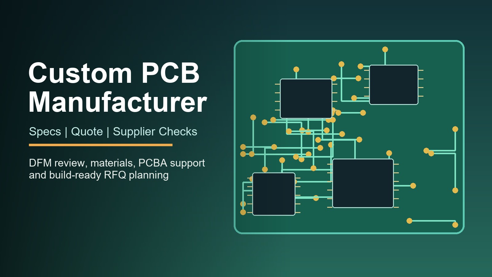
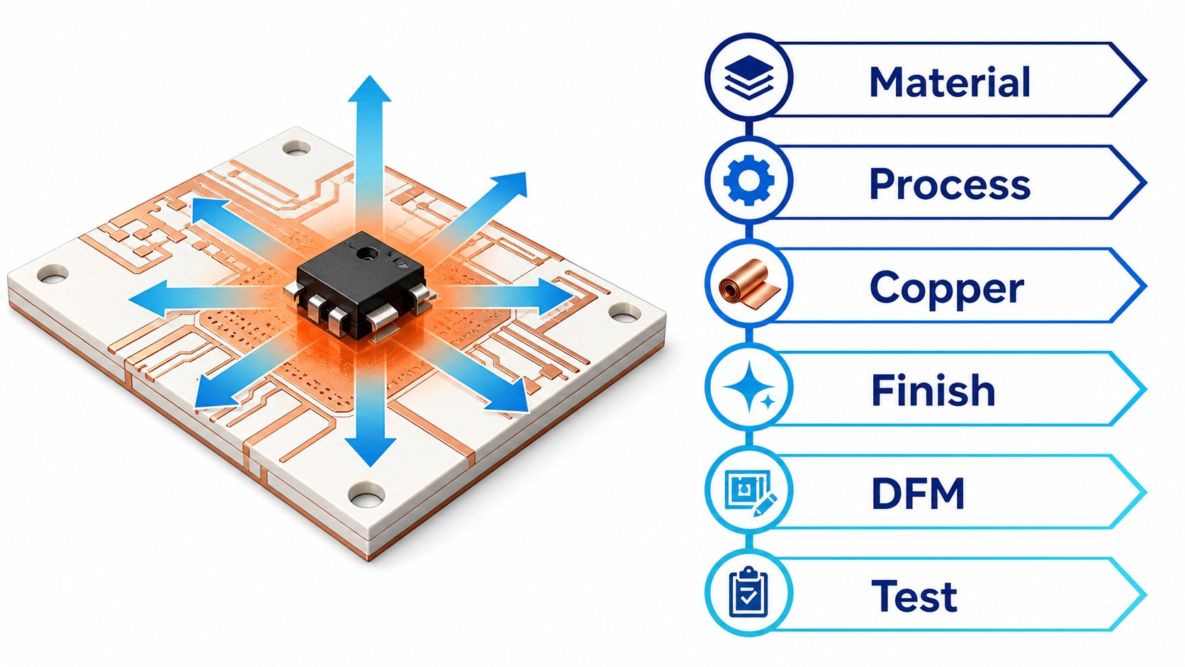
A custom PCB manufacturer should do more than make a board from Gerber files. The right partner checks stackup, materials, copper weight, drill data, surface finish, solder mask, panelization, assembly needs, testing requirements and quote assumptions before production starts.
For buyers, the real decision is not simply which factory can produce the lowest unit price. It is whether the manufacturer can turn your design files into reliable boards with the right manufacturing route, clear DFM feedback, stable quality controls and enough support for prototype, small-batch or production orders.
Before choosing a custom PCB manufacturer, check whether your quote package is truly build-ready.
Custom PCB orders often fail at the handoff between design, quotation and production. Buyers should check these risks early:
The supplier quotes a standard board even though the design needs special material, controlled impedance, heavy copper, HDI, flex, rigid-flex, metal core or ceramic review.
The Gerber, drill, stackup and fabrication drawing do not describe the same board.
The quote excludes assembly, BOM review, CPL data, testing, programming, conformal coating or packaging requirements that affect the real project cost.
The manufacturer accepts files without flagging spacing, annular ring, solder mask, copper balance, panelization or tolerance risks.
The buyer compares suppliers only by unit price and misses quality evidence, communication speed and engineering support.
EBest Circuit supports custom PCB projects with DFM review, manufacturing and optional PCBA coordination.
We review Gerber, ODB++, drill files, stackup, fabrication drawings, BOM and CPL files when the project requires a complete PCB or PCBA quotation.
We help buyers confirm material, copper, surface finish, board thickness, impedance, solder mask, panelization and testing requirements before production release.
We support custom discussions across FR4, HDI, heavy copper, metal core, ceramic, flex and rigid-flex PCB categories when the files need project-specific confirmation.
We keep the RFQ discussion focused on build risk, quality controls and realistic project scope instead of only a unit-price comparison.
Custom PCB Manufacturer in One Practical Answer
A custom PCB manufacturer builds boards to project-specific files, materials, dimensions, stackups and quality requirements rather than a fixed catalog design. The manufacturer should review whether the design can be fabricated, assembled, inspected and delivered under the requested conditions.
This article is written for engineers, sourcing teams and product teams comparing custom printed circuit board manufacturers for prototypes, engineering builds, low-volume production or supplier qualification.
When Do You Need a Custom PCB Manufacturer Instead of a Standard PCB Order?
You need a custom PCB manufacturer when the board has requirements that a simple online quote form cannot fully judge. Examples include tight spacing, high layer count, impedance control, unusual thickness, heavy copper, RF laminate, thermal substrate, bend areas, assembly constraints or specific inspection requirements.
If your board is a basic two-layer FR4 prototype, a simple quote tool may be enough. If the board affects heat, signal integrity, fit, vibration, enclosure assembly, compliance documentation or field reliability, the manufacturer should review the files before price becomes the only decision.
What Buyers Should Check Before Sending Files
The best supplier comparison starts with a clean file package and a clear definition of what must be built. A manufacturer cannot quote accurately if the board data, material request, finished thickness, copper weight, surface finish and assembly scope are incomplete or contradictory.
Buyer Check
Why It Matters
What to Send
Board data
Defines the physical circuit
Gerber or ODB++, drill, outline and fab notes
Stackup
Affects impedance, thickness, lamination and cost
Layer order, dielectric targets and copper weight
Material
Controls thermal, RF, flex or reliability behavior
FR4 grade or special material request
Assembly scope
Changes BOM, CPL, stencil, inspection and testing
BOM, CPL, assembly drawing and test notes
Acceptance criteria
Reduces disputes after delivery
IPC class, inspection needs and special notes
How EBest Circuit Supports Custom PCB Manufacturing Projects
EBest Circuit can review custom PCB projects from the manufacturing route through optional PCBA support. The useful starting point is a complete RFQ package, not a vague board description.
For broader capability context, buyers can review EBest Circuit’s PCB manufacturing capabilities. If a project needs assembly, the PCBA and SMT assembly support page helps connect fabrication with component mounting and production planning.
Specifications a Custom PCB Manufacturer Must Confirm
A reliable custom PCB quote should confirm the board specifications that affect manufacturability, cost and risk. At minimum, the discussion should cover layer count, finished thickness, copper weight, minimum trace/space, minimum finished hole, solder mask, silkscreen, surface finish, impedance and panelization.
Some specifications are standard for one factory but special for another. Treat special materials, unusual copper, tight tolerance, HDI, metal core, ceramic, flex or rigid-flex requirements as project-confirmation items rather than assumptions.
Prototype, Small Batch and Production Fit
The right custom PCB manufacturer should match the order stage: prototype, engineering validation, small batch or production. Prototype builds usually prioritize DFM feedback and fast learning, while production builds need stable documentation, repeatable inspection and clear change control.
Buyers should ask whether the quote supports only bare boards or also future assembly, test fixtures, packaging and repeat ordering. A low prototype price can become expensive if the supplier cannot support the next build stage.
Need a custom PCB quote checked before production?
Send Gerber or ODB++, drill, stackup, drawing, quantity and any assembly notes. EBest Circuit can review the build risk and quote scope before you commit.
Gerber/ODB++ | Drill | Stackup | Drawing | BOM/CPL if assembly is needed
Materials, Stackup and Copper Choices
Material, stackup and copper decisions should be confirmed before comparing supplier prices. FR4 remains common for many boards, while special projects may require high Tg FR4, RF laminate, aluminum, copper base, ceramic, flex or rigid-flex structures.
For FR4-related project planning, see EBest Circuit’s FR4 PCB material options. For any special material or tight process requirement, the safest wording is project confirmation: send the files and ask the manufacturer to verify whether the requested construction is standard, special or not recommended.
DFM Review Before Custom PCB Fabrication
DFM review catches manufacturing risk before CAM release, procurement and production scheduling. It should check spacing, annular ring, drill aspect ratio, copper balance, solder mask bridge, silkscreen clearance, board outline, panel rail, fiducials and test access.
A good DFM review does not replace the engineer’s design responsibility. It helps identify file conflicts and production risks early enough to revise the layout, change a material assumption or clarify a tolerance before the order is released. For a connected view of design release and production planning, see the PCB design and manufacturing workflow.
PCBA, BOM and Component Sourcing Support
If the finished product needs assembly, the custom PCB quote should include PCBA assumptions early. Bare-board fabrication and assembly are connected by pad design, solder mask, stencil openings, component availability, CPL accuracy, inspection method and test requirements.
When a project includes assembly, ask the manufacturer to review BOM, CPL, assembly drawing, polarity notes, special components, programming and functional test expectations together with the bare board files.
Quality, Inspection and Testing Evidence
Quality evidence matters more than broad claims such as “high quality” or “best manufacturer.” Ask what inspection steps apply to your board type: electrical test, AOI, X-ray for hidden solder joints, impedance report, first article review, final visual inspection or functional test when the project requires it.
The exact evidence should match the order. A simple bare board does not need the same proof package as a high-density assembly, and a prototype may need different documentation than a repeat production run.
Cost Drivers in a Custom PCB Quote
Custom PCB cost changes when the design requires more material control, process complexity, inspection effort or assembly coordination. Main drivers include layer count, board size, material, copper weight, minimum trace/space, finished hole size, surface finish, impedance, routing, quantity, testing and PCBA scope.
Do not compare suppliers only by the first quoted unit price. Compare what is included, what is excluded, what requires engineering confirmation and what happens if files need revision after DFM review.
A complete RFQ package reduces quote delay and prevents mismatched assumptions. Send the manufacturer enough information to identify the board, build route, inspection needs and commercial scope.
Gerber or ODB++ files and NC drill data.
Fabrication drawing with board thickness, copper, finish, tolerance and notes.
Stackup and impedance targets when required.
Quantity, target date and prototype or production stage.
BOM, CPL, assembly drawing and test plan if PCBA is included.
Special material, thermal, high-current, flex, rigid-flex, ceramic or metal-core requirements.
Red Flags When Comparing Custom PCB Manufacturers
Supplier red flags usually appear before production if buyers ask the right questions. Be careful when a manufacturer quotes without checking files, gives a very low price with unclear exclusions, avoids DFM discussion, cannot explain inspection steps or pushes all responsibility back to the buyer after file upload.
Price, speed, location and past supplier experience are useful comparison points, but the final decision should still depend on the board’s engineering risk and the supplier’s ability to support your exact build.
Add EBest Circuit to your custom PCB RFQ shortlist.
Let our team review the files, quote assumptions and assembly needs so you can compare suppliers on manufacturability, quality control and real project scope.
The final supplier decision should be based on build fit, evidence and communication clarity. Before approving a custom PCB manufacturer, ask direct questions that reveal whether the supplier understands your project.
Which specifications are standard, special or need engineering confirmation?
What DFM issues should be corrected before production?
Which material, copper and surface finish options fit the application?
What inspection or test evidence will be supplied?
Does the quote include only bare boards, or also assembly, BOM review and testing?
What information is still missing from the RFQ package?
Custom PCB Manufacturer FAQ
What is a custom PCB manufacturer? A custom PCB manufacturer builds printed circuit boards from project-specific design files, materials, dimensions, stackups and production requirements. The supplier should confirm manufacturability before fabrication.
Is a custom PCB manufacturer different from a PCB maker? Sometimes the terms overlap. In buying decisions, a custom PCB manufacturer usually implies stronger file review, process confirmation, material choice, quality control and project support than a simple hobby PCB maker.
What files are needed for a custom PCB quote? Send Gerber or ODB++, NC drill, fabrication drawing, stackup, quantity and special requirements. For assembly, also send BOM, CPL, assembly drawing, test notes and programming requirements if applicable.
Can a custom PCB manufacturer also assemble the board? Some manufacturers can coordinate PCBA, while others only fabricate bare boards. Confirm BOM review, CPL review, SMT, through-hole, inspection and testing scope before comparing quotes.
Final Recommendation
Choose a custom PCB manufacturer that can prove fit for your board, not just quote the lowest price. The strongest RFQ process starts with complete files, clear specifications, DFM review, quality evidence and a supplier that can support the project stage you are actually building.
Send your Gerber or ODB++, drill files, stackup, fabrication drawing, quantity, target schedule and BOM/CPL if assembly is needed to sales@bestpcbs.com. EBest Circuit can review your custom PCB manufacturing requirements and provide a practical quotation path for bare boards, PCBA or build-ready projects.
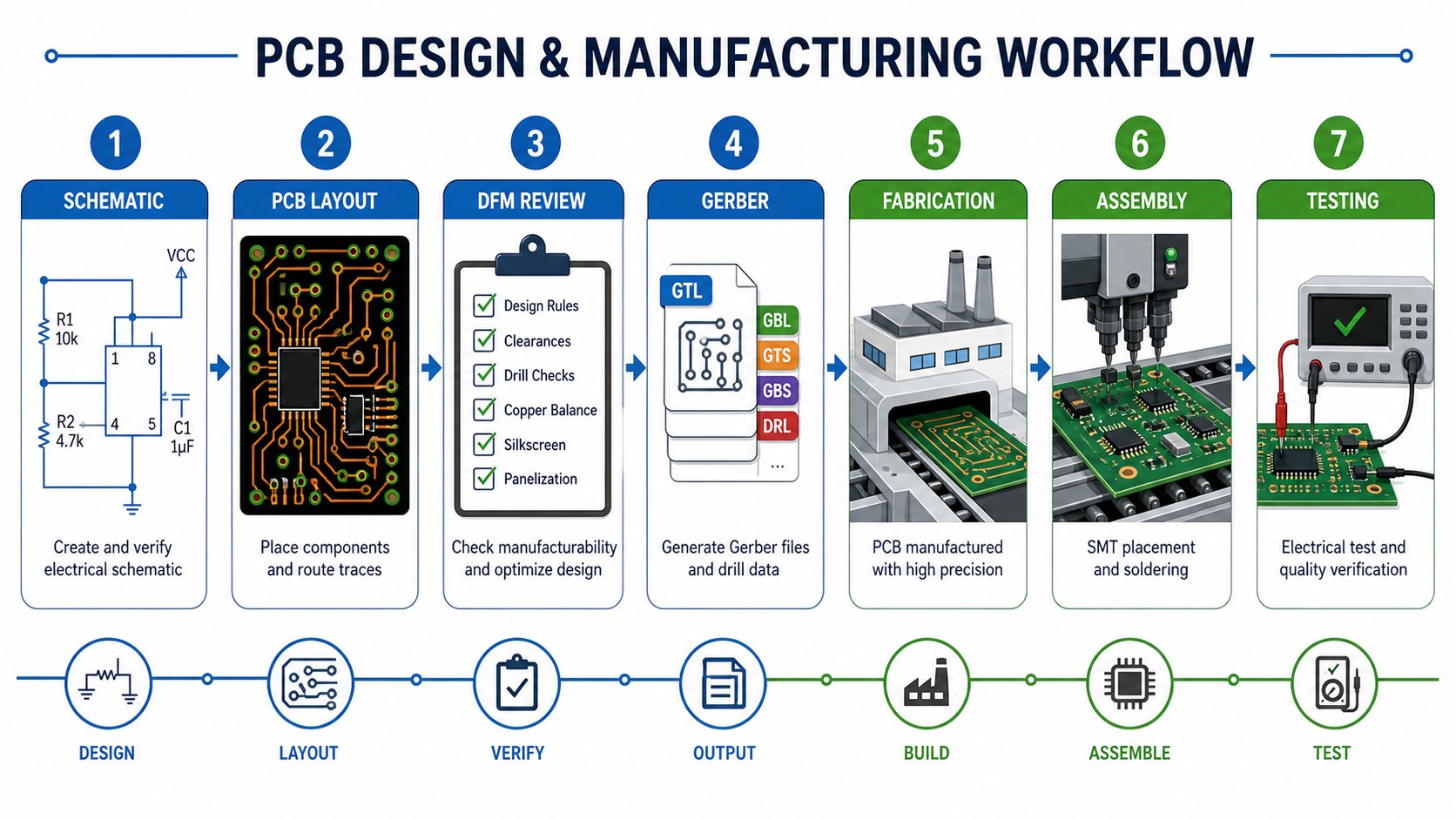
PCB design and manufacturing should be planned as one workflow, not two separate jobs. A board layout that looks complete in CAD can still fail manufacturing review if the stackup, copper, spacing, drill, solder mask, panelization, assembly access or test points are not checked before release.
For buyers and engineers, the safest path is simple: design the circuit, review the board for manufacturability, export complete files, then quote fabrication and assembly with the same technical assumptions. EBest Circuit helps customers connect DFM review, bare board production and optional PCBA so fewer problems move from design files into production.
Is your PCB design ready for manufacturing, or only ready for export?
Many projects reach RFQ stage with files that look finished but still hide production risk:
Trace spacing, drill size or annular ring is too aggressive for the selected copper weight.
The stackup does not match the requested material, board thickness or impedance target.
Silkscreen, solder mask openings or component courtyards create assembly problems.
Panelization, fiducials and test points are missing, so manufacturing and assembly teams must guess.
The supplier quotes only the bare board while BOM, CPL and testing needs are handled too late.
EBest Circuit reviews design files through a manufacturing and assembly lens.
We check Gerber, drill, drawing, stackup, copper, solder mask and surface finish before production release.
We flag manufacturability risks that can affect fabrication, SMT assembly, through-hole assembly or testing.
We support FR4, HDI, heavy copper, metal core, ceramic, flex and rigid-flex project discussions when files require more than standard review.
We can quote bare boards and PCBA together when the project needs BOM, CPL and assembly drawing review.
PCB Design and Manufacturing in One Practical Answer
PCB design defines the circuit layout, while PCB manufacturing turns that layout into a physical board; the two must be checked together through DFM review. Good design-for-manufacturing work reduces redesign, quote changes, production delay and assembly risk.
Why Design Files Fail at Manufacturing Stage
Design files usually fail because electrical layout choices were not checked against real fabrication limits. Common examples include too-small vias, narrow solder mask bridges, copper imbalance, unclear board outline, missing drill tables and incomplete fabrication notes.
A useful RFQ package tells the manufacturer not only what the circuit is, but how it should be built, finished, inspected and assembled.
DFM Review Before PCB Manufacturing
DFM review checks whether a PCB layout can be built reliably before CAM work and production begin. It should cover stackup, material, copper, minimum trace and space, hole type, annular ring, solder mask, silkscreen, outline, panelization and test access.
Stackup, laminate and copper should be locked before the buyer compares prices. FR4 material may use low Tg, mid Tg or high Tg options, while special projects may need Rogers, PTFE, ceramic, aluminum or other materials. Copper weight affects spacing, heat rise, plating, etching and cost.
For FR4 project context, see the FR4 PCB capability page.
Layout Checks That Protect Fabrication
The most important fabrication checks are trace width, spacing, drill size, annular ring, copper-to-edge clearance and solder mask bridge. These details decide whether the board can be built as standard or needs special confirmation.
Design Item
Manufacturing Risk
Buyer Action
Trace / spacing
Etching or solder bridge risk
Match rules to copper weight
Drill / pad
Weak plated hole or breakout
Check finished hole and annular ring
Board outline
Routing, V-cut or enclosure fit issue
Send mechanical drawing
Solder mask
Assembly yield risk
Review openings and bridges
Panelization
Cost and handling changes
Confirm rail, fiducial and breakaway needs
Need a DFM check before PCB manufacturing?
Send Gerber, drill, stackup, drawing, quantity and assembly notes. EBest Circuit can review the files before quote and production release.
A practical PCB workflow connects schematic, layout, DFM, Gerber files, fabrication, assembly and testing.
Gerber, Drill, Drawing and BOM Package
A complete file package reduces quote changes and manufacturing questions. For bare boards, send Gerber or ODB++, NC drill, drawing, stackup, material, copper, finish, quantity and test requirements. For assembly, add BOM, CPL, assembly drawing and approved substitutions.
PCB Fabrication Process After Design Release
After release, fabrication moves through CAM review, material preparation, imaging, drilling, plating, etching, solder mask, surface finish, profiling, inspection and electrical test. The cleaner the design package is, the fewer decisions need to be corrected during CAM.
Assembly planning should start during layout, not after bare boards arrive. Component spacing, polarity marks, fiducials, test pads, panel rails and connector orientation all affect SMT and through-hole production.
If your project needs turnkey support, EBest Circuit can review fabrication data together with BOM and CPL. See our PCBA service.
Testing and Quality Checks
Testing confirms whether the design intent survived manufacturing and assembly. Bare boards may need electrical test for opens and shorts. Assemblies may need AOI, functional testing, programming, inspection reports or project-specific test fixtures.
Cost Drivers From Design to Manufacturing
Cost is shaped by design choices before the RFQ is sent. Layer count, board size, material, copper weight, surface finish, drill count, tolerance, impedance, solder mask, test method, assembly complexity and quantity all affect the final quote.
When to Move From Two Layers to Multilayer
Move to multilayer PCB when routing density, signal return, power integrity or impedance control cannot be handled safely on one or two copper layers. Staying with too few layers can create more cost through redesign and debugging than the stackup saves.
Supplier Questions Before Sending the Order
Ask questions that reveal whether the supplier can connect design review with real production.
Can you review DFM before formal production release?
Which design rules change with copper weight and surface finish?
Can you quote bare PCB and PCBA from the same file package?
What files are missing for a reliable manufacturing quote?
Will you flag assembly and testing risks before boards are built?
RFQ Checklist for PCB Design and Manufacturing
The RFQ should include enough information for engineering review, not only price calculation.
Gerber or ODB++ files
NC drill file and fabrication drawing
Stackup, material, board thickness and copper weight
Surface finish, solder mask and silkscreen notes
Quantity, target schedule and testing requirements
BOM, CPL and assembly drawing if PCBA is needed
FAQ About PCB Design and Manufacturing
These questions help buyers connect layout decisions with manufacturing results.
What is PCB design and manufacturing?
PCB design creates the circuit layout, and PCB manufacturing fabricates that design into a physical board through material preparation, drilling, plating, etching, solder mask, finish and test.
Why is DFM important before PCB manufacturing?
DFM review finds layout and file issues before production, reducing redesign, delay, quote changes and assembly risk.
Can EBest Circuit review my PCB design before quote?
Yes. Send Gerber, drill, drawing, stackup and project notes, and EBest Circuit can review the file package before preparing the manufacturing scope.
Can PCB design and assembly be reviewed together?
Yes. When PCBA is required, send BOM, CPL and assembly drawings with the PCB files so fabrication and assembly risks can be checked together.
Final Recommendation
Treat PCB design and manufacturing as one connected engineering path. The best time to control cost, schedule and quality is before files enter production, when DFM, material, copper, drill, finish, assembly and testing can still be aligned.
To review a PCB design and manufacturing project with EBest Circuit, send Gerber or ODB++, NC drill, fabrication drawing, stackup, material, copper, finish, quantity, target schedule and any BOM/CPL files to sales@bestpcbs.com. Our team will check manufacturability and prepare a practical quote scope.
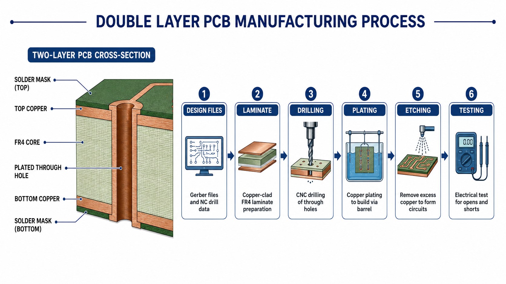
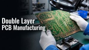
Double layer PCB manufacturing builds a printed circuit board with copper circuitry on both sides of an insulating core, connected by plated through holes. It is often the best choice when a single-sided board cannot route the circuit cleanly, but the project does not yet need the cost, stackup control or density of a multilayer PCB.
For buyers, the real decision is not only whether the board has two copper layers. The safer question is whether your manufacturer can review the Gerber data, copper weight, drill file, annular ring, solder mask, surface finish, test method and assembly needs before fabrication starts. That review is where many two-layer boards either become easy to build or quietly turn into delay, rework and cost.
Is your double layer PCB order getting stuck before production?
Many two-layer boards look simple on the purchase order, but the issues usually appear inside the fabrication files:
Through-hole pads are too small for the drill tolerance, leaving weak annular rings after plating.
Trace width and spacing are copied from a prototype tool without checking the finished copper weight.
The stackup does not leave enough board thickness, copper balance or mechanical margin for the enclosure.
Solder mask openings, bridges and silkscreen markings are not matched to the assembly process.
The RFQ only asks for a unit price, so the supplier does not review test points, panelization or PCBA risk early enough.
EBest Circuit helps buyers turn a two-layer PCB file into a build-ready order.
We review Gerber, drill, drawing and stackup details before production release.
We check copper weight, hole plating, solder mask bridge, outline and finish choices against manufacturability.
We support bare board fabrication and optional PCBA so layout, fabrication and assembly risks can be handled together.
We help buyers normalize quotes by board thickness, finish, test method, panelization and order quantity instead of comparing unit price alone.
We keep the project discussion practical: what can be built as standard, what needs confirmation, and what should be corrected before the order starts.
Double Layer PCB Manufacturing in One Practical Answer
Double layer PCB manufacturing is the process of making a board with top and bottom copper layers connected by plated through holes. It is used for control boards, power interfaces, LED drivers, sensor boards, industrial electronics, consumer products and many PCBA projects where routing on one side is not enough.
A two-layer PCB normally gives more routing freedom than a single-sided board, better grounding options, shorter jumper paths and easier component placement. Compared with multilayer PCB manufacturing, it usually keeps the stackup simpler and the cost easier to control.
When a Two-Layer PCB Is the Right Build
A two-layer PCB is right when the design needs routing on both sides but does not require controlled multilayer power planes or very high density. It is a common fit for moderate-density components, connectors on both sides, low-to-medium speed signals, simple power paths and production boards that need reliable plated vias.
If your board has dense BGA escape, strict impedance control, high-speed interfaces or multiple isolated power domains, a multilayer stackup may be safer. If the circuit is very simple and one side can route cleanly, a single-sided board may still be enough. The best choice comes from routing, copper, assembly and test requirements together.
What Buyers Need to Control Before Fabrication
The most important buyer controls are copper weight, minimum trace and spacing, hole size, annular ring, board thickness, finish and test coverage. These items decide whether a two-layer board can be produced as a standard order or needs engineering confirmation.
RFQ Item
Why It Matters
What to Send
Copper weight
Affects trace width, heat rise, etching and price
Finished copper requirement for each side
Drill file
Controls plated through holes and component fit
NC drill file plus finished hole notes
Board thickness
Affects rigidity, connector fit and V-cut planning
Drawing or stackup note
Surface finish
Affects soldering, storage and contact reliability
OSP, HASL, ENIG or other finish choice
Testing
Confirms opens, shorts and production reliability
Electrical test and special inspection needs
How EBest Circuit Reviews a Two-Layer PCB Order
EBest Circuit reviews a two-layer PCB order by connecting the drawing, Gerber, drill data, copper, finish and assembly plan before quoting. This avoids a quote that looks attractive but misses the details that later change production cost or yield risk.
For a typical order, we check whether the design fits the requested material, whether copper and spacing are realistic, whether the drill and pad design support reliable plating, whether panelization will affect outline quality, and whether the finished board can support the assembly process.
Ready to quote a double layer PCB?
Send Gerber, NC drill, drawing, copper weight, finish, quantity and assembly notes. EBest Circuit will review the files before preparing a practical RFQ response.
A double layer PCB stackup normally places copper on both sides of an FR4 core, with plated holes joining the two copper layers. This structure gives the designer more options for routing signals, distributing power and creating return paths.
For low-speed control electronics, one side may carry most routing while the other side supports power and ground paths. For power or LED circuits, copper width, heat path and via placement become more important. For assembly-heavy designs, component placement and test access may matter more than the copper layers themselves.
FR4 Materials, Tg Options and Copper Weight
FR4 material and copper weight should be selected before price comparison, because both change how the board is built. EBest Circuit capability records include FR4 low Tg, mid Tg, high Tg and special material options, and list FR4 high-Tg layer capability from 1-10 layers as a general range with special review for higher layer counts.
For copper, the capability records list FR4 inner copper from HOZ-5OZ as general capability and 5-20OZ as special review; FR4 outer copper is listed from 1OZ-5OZ as general capability and 5-20OZ as special review. A two-layer board with heavy copper should therefore be checked for spacing, etching, solder mask bridge and heat requirements before order release.
Board Thickness, Panel Size and Finish Choices
Board thickness and surface finish should be matched to soldering, mechanical fit and expected handling. Capability records list common processed thickness ranges by finish, including OSP, ENIG, immersion silver, immersion tin and ENEPIG from 0.4-3.5 mm, and HASL from 0.6-3.5 mm. Boards outside the common range need project confirmation.
Finish choice should not be made only by habit. OSP can suit cost-sensitive soldering projects. HASL may fit many conventional through-hole or hand-soldered boards. ENIG is often chosen when flat pads, storage or fine assembly behavior matter. The right finish depends on assembly, storage, contact needs and cost.
Line Width, Spacing, Drill and Annular Ring Checks
Two-layer boards often fail manufacturability review at trace spacing, drill size or annular ring, not at the layer count itself. EBest Circuit capability data lists example FR4 line and space capability such as 4/4 mil general and 3/3 mil special for common copper examples, but the final check depends on copper thickness, board finish and design context.
For plated through holes, do not compare only the nominal drill diameter. The finished hole, plating allowance, pad size, annular ring and tolerance all need to work together. If the pad is too small, the board may pass a visual check but still carry long-term reliability risk.
Double layer PCB manufacturing connects stackup, drilling, plating, etching and electrical testing into one build path.
Double Layer PCB Manufacturing Process
The core process includes file review, laminate preparation, drilling, copper plating, imaging, etching, solder mask, surface finish, routing and electrical test. The process is simple to describe, but each step depends on the files and requirements supplied at RFQ stage.
File review: Gerber, NC drill, drawing, stackup, quantity and finish are checked.
Laminate preparation: FR4 copper-clad material is selected and prepared.
Drilling: through holes, mounting holes and slots are drilled according to the NC file.
Plating: copper is deposited in through holes to connect top and bottom layers.
Imaging and etching: unwanted copper is removed to form the circuit pattern.
Solder mask and legend: mask openings and silkscreen are applied and checked.
Surface finish: pads receive OSP, HASL, ENIG or another specified finish.
Routing and test: boards are profiled, inspected and electrically tested.
Plated Through Hole Quality and Via Reliability
Plated through hole quality is one of the most important reliability checks in double layer PCB manufacturing. Every signal or power path that moves from top to bottom depends on drilled hole quality, plating coverage and pad design.
Buyers should identify high-current vias, connector holes, thermal vias and mechanically stressed holes in the drawing or notes. These areas may need larger pads, stronger copper, better test coverage or a DFM correction before manufacturing.
Solder Mask, Silkscreen and Surface Finish Decisions
Solder mask and surface finish affect assembly reliability as much as board appearance. The solder mask must leave enough bridge between pads, avoid unwanted exposed copper and match the assembly process. Silkscreen should remain readable without crossing pads or tight components.
EBest Circuit capability data lists solder mask color options and common surface finishes including OSP, HASL, ENIG, immersion silver, immersion tin, ENEPIG and hard gold fingers. The final finish should be chosen by soldering method, storage life, pad flatness and contact needs.
Cost Drivers in Two-Layer PCB Manufacturing
The main cost drivers are material, board size, copper weight, thickness, finish, drill count, tolerance, test coverage, panelization and quantity. A low unit price is not useful if it leaves out electrical testing, special finish, assembly support or engineering review.
Cost Factor
Typical Impact
Buyer Check
Board size
Larger panels consume more laminate
Confirm dimensions and panel quantity
Copper weight
Higher copper affects etching and spacing
State finished copper clearly
Surface finish
ENIG and special finishes usually change cost
Choose finish by assembly need
Drilling
More holes and smaller holes add process load
Send NC drill and finished hole notes
Testing
Electrical test prevents hidden opens and shorts
Include test requirement in RFQ
Prototype, Low-Volume and Production Planning
Prototype and production orders should use the same key manufacturing assumptions whenever possible. If the prototype uses one finish, copper weight or stackup and production changes another, the test result may not represent the final board.
For early builds, a practical plan is to lock the stackup, copper and finish early, then use DFM feedback to adjust holes, pads, solder mask and panelization before larger production. For related prototype planning, see our prototype PCB manufacturing guide.
Double Layer PCB Assembly Support
Two-layer PCB manufacturing should be reviewed with assembly in mind when the board will become a PCBA. Component orientation, test points, solder mask openings, via placement and connector fit can all affect assembly yield.
If EBest Circuit handles both bare board and assembly review, the team can check Gerber data together with BOM, CPL, assembly drawing and testing needs. This is especially useful for connectors, through-hole parts, mixed SMT/THT assemblies and boards with high-current paths. For assembly support, see our PCBA service.
Need bare board plus assembly support?
Share Gerber, BOM, CPL, drawings, quantity and test requirements. We can review the two-layer board and PCBA plan together before quoting.
Electrical testing should be part of a serious double layer PCB manufacturing order. It helps detect opens, shorts and connectivity problems before boards move to assembly or final product testing.
Inspection should also cover solder mask registration, surface finish, hole condition, outline quality and key dimensions. If the board carries power, connectors or field-service risk, mark those features in the drawing so the supplier can understand what matters most.
Double Layer PCB vs Single Layer and Multilayer PCB
A double layer PCB sits between single-sided simplicity and multilayer routing density. It gives more routing freedom than one-sided construction while keeping the manufacturing path simpler than four-layer or higher stackups.
Board Type
Best Fit
Main Limitation
Single layer PCB
Very simple circuits and low cost boards
Limited routing flexibility
Double layer PCB
General electronics, connectors, moderate routing and PCBA
No internal planes for dense routing
Multilayer PCB
High density, power planes, impedance and complex routing
Higher stackup and fabrication complexity
For broader board selection, the FR4 PCB product page and our double-sided PCB boards article provide related background.
Supplier Questions Before Purchase Order
Before placing a purchase order, ask questions that expose engineering fit, not only price. A reliable supplier should be able to discuss manufacturability, testing and assembly impact in plain terms.
If the order is only for bare boards before assembly, it also helps to compare the quote against a dedicated bare PCB manufacturer RFQ checklist so board fabrication, testing and documentation are reviewed before components enter the project.
Can you review Gerber, NC drill and drawing before production release?
What copper weight, trace spacing and board thickness need special confirmation?
Which surface finish best matches my assembly and storage needs?
Will the quote include electrical testing and inspection requirements?
Can you support bare PCB fabrication and assembly if the project moves to PCBA?
RFQ File Checklist for Double Layer PCB Manufacturing
A complete RFQ package lets the manufacturer quote the same board you actually need built. Missing drill data, unclear copper weight or vague testing notes can produce a fast quote that later changes.
Gerber files or ODB++ package
NC drill file and finished hole notes
Board drawing with dimensions, tolerance and thickness
Material, Tg, copper weight and surface finish requirements
Quantity, panelization preference and target schedule
Electrical test, inspection or special reliability requirements
BOM, CPL and assembly drawing if PCBA is required
FAQ About Double Layer PCB Manufacturing
These questions cover the decisions buyers usually need to settle before quoting a two-layer PCB.
What is double layer PCB manufacturing?
Double layer PCB manufacturing makes a board with copper circuits on the top and bottom sides of an insulating core, connected by plated through holes.
Is a double layer PCB the same as a double-sided PCB?
In most buying and manufacturing discussions, yes. Both terms usually refer to a board with copper features on both sides.
What files are needed for a double layer PCB quote?
Send Gerber or ODB++, NC drill, drawing, material, copper, thickness, finish, quantity, test needs and assembly files if PCBA is required.
What affects double layer PCB price most?
Board size, copper weight, thickness, finish, hole count, tolerance, test coverage, panelization and quantity usually drive price.
Can EBest Circuit assemble double layer PCBs?
Yes. EBest Circuit can review double layer PCB fabrication together with BOM, CPL, assembly drawing and testing requirements when PCBA support is needed.
Final Recommendation
Choose double layer PCB manufacturing when the board needs more routing and reliability than a single-sided PCB, but does not need a multilayer stackup. The best result comes from aligning copper, holes, finish, solder mask, test and assembly before fabrication starts.
To quote a double layer PCB project with EBest Circuit, send Gerber or ODB++, NC drill, drawing, board thickness, copper weight, surface finish, quantity, testing notes, target schedule and any BOM/CPL files to sales@bestpcbs.com. Our team will review the build path, check manufacturability and prepare a practical quotation scope.
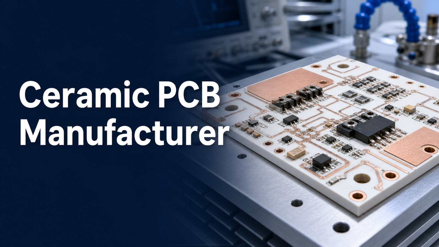
A ceramic PCB manufacturer should help you choose the right substrate, ceramic process, copper structure, surface finish, DFM limits, assembly path and test plan before you place the order. Ceramic boards are not selected only because they look more advanced than FR4. They are used when heat, insulation, high temperature, power density, RF behavior, dimensional stability or long-term reliability makes an organic laminate a poor fit.
EBest Circuit supports buyers with ceramic PCB manufacturing, DFM review, material and process confirmation, optional ceramic PCB assembly, BOM/CPL review and RFQ planning. Send your Gerber or ODB++, drawing, stackup, substrate request, copper requirement, finish, quantity, assembly files and test needs early so the project can be reviewed as a ceramic substrate build rather than a normal PCB quote.
Ceramic Board Buyer Decision Before Quote Approval
A ceramic PCB manufacturer should first help you decide whether the project needs alumina, aluminum nitride, ZTA, silicon nitride, DPC, DBC/DCB, AMB, thick film, LTCC or HTCC. The right answer depends on heat flow, conductor thickness, layer count, operating environment, part mounting, dimensional limits and cost target.
Many ceramic PCB delays happen because the RFQ says only “ceramic PCB” without defining the substrate and process. That is not enough. A thin film ceramic circuit, a DPC board, a DBC/DCB power substrate and an AMB ceramic board do not follow the same design rules or quote logic.
Is your ceramic PCB quote difficult to compare because every supplier is reading the files differently?
Buyers often run into these problems before a ceramic PCB order is approved:
The project asks for a ceramic PCB, but the substrate material and ceramic process are not clearly tied to the thermal or electrical requirement.
The copper thickness looks attractive in a quote, but trace width, spacing, panel size, edge quality and assembly clearance have not been reviewed together.
The board needs good heat transfer, yet the RFQ does not show the heat source, heat path, mounting surface or expected test condition.
The same design is sent to FR4, MCPCB and ceramic PCB suppliers without adjusting design rules, creating slow DFM loops.
Assembly, component sourcing and test requirements arrive after fabrication planning, forcing late changes to pads, finish, fixtures or packaging.
Five RFQ Details That Change a Ceramic Board Build
Ceramic PCB projects often get delayed when the purchase team compares unit prices before engineering has confirmed the substrate, conductor, finish and test scope. A low line-item price can hide a weak quote if the supplier has not checked manufacturability.
For a buyer, the fastest path is to make the quote package specific. Show where the heat enters the ceramic substrate, which components sit on high-copper areas, whether the board needs assembly, which finish is expected, and what inspection or reliability checks are important for the application.
EBest Circuit helps turn ceramic PCB uncertainty into a reviewable RFQ package:
We review substrate choice, ceramic process, copper thickness, line/space, hole design, finish and board outline together instead of quoting one isolated specification.
We separate standard capability, special review items and file-dependent limits so buyers do not approve a quote on unsupported assumptions.
We connect ceramic PCB fabrication with PCBA planning when pads, power devices, thermal interfaces, component sourcing or test fixtures affect the finished product.
We help buyers compare quote scope, not only unit price, so prototype and production decisions are easier to defend internally.
EBest Circuit Review Path for Ceramic Substrate Orders
EBest Circuit reviews ceramic PCB projects by checking substrate, process, copper, geometry, finish, assembly and test requirements before production planning. This reduces the chance that a quote looks acceptable but later fails during DFM, assembly or reliability review.
For example, a high-power ceramic board may need DBC/DCB ceramic PCB or AMB discussion because conductor thickness and heat transfer are more important than fine traces. A precision circuit may need DPC or thin film review because line/space, metallization and surface quality matter more. The right manufacturing route should be selected from the function of the board, not from a catalog word.
Ready to Review a Ceramic PCB Build?
Send your substrate choice, Gerber or ODB++, drawing, copper requirement and assembly scope for a practical DFM and RFQ review.
DFM review | BOM/CPL check | Fabrication and assembly planning
When Ceramic Beats FR4 or Metal Core PCB
Ceramic PCB is usually the right choice when the board needs stronger heat transfer, electrical insulation, dimensional stability or high-temperature performance than a normal FR4 board can provide. It is not the lowest-cost route for every circuit, but it can be the better route when thermal or reliability risk dominates the project.
Project Need
Why Ceramic PCB May Fit
What to Confirm Before RFQ
High heat density
Ceramic substrates can support strong heat transfer paths.
Heat source, substrate, copper thickness and mounting method.
Power electronics
DBC/DCB or AMB structures can support thicker conductors.
Copper weight, isolation, outline, finish and test needs.
RF or high-frequency circuit
Some ceramic materials offer stable dielectric behavior.
Material, impedance target, geometry and finish.
Harsh or high-temperature environment
Ceramic substrates can provide heat and chemical stability.
Operating temperature, coating, metallization and reliability checks.
Alumina, AlN, ZTA and Si3N4 Board Fit
Ceramic PCB material should be selected from thermal, mechanical, electrical and cost requirements, not from the keyword alone. Verified EBest Circuit capability records list ceramic substrate options including Al2O3, AlN, ZTA and Si3N4. Special substrate discussions may also involve glass, quartz, sapphire and different alumina grades depending on the project.
Alumina is common in ceramic circuit projects because it balances insulation, availability and cost. Aluminum nitride is often considered when thermal performance is a bigger driver. ZTA and silicon nitride can enter the discussion when mechanical strength, hardness or stability matter. Each choice should be checked with board thickness, conductor method, outline and test requirements.
DPC, DBC, AMB, Thick Film, LTCC and HTCC Routes
The ceramic PCB process should match the required copper structure, layer count, thermal path and operating environment. The source capability records include DPC, DBC/DCB, AMB, thick film, LTCC and HTCC, but they are not interchangeable processes.
Process
Typical Buying Question
RFQ Evidence Needed
DPC
Do I need finer ceramic circuit features?
Line/space, conductor thickness, finish and dimensional drawing.
DBC/DCB
Do I need a strong direct copper thermal path?
Copper thickness, substrate, isolation, power device location.
Does the design need a ceramic circuit route beyond common DPC/DBC?
Layer count, conductor material, application conditions and drawings.
Layer Count and Panel Size by Ceramic Route
Layer count, copper thickness and panel size must be checked by ceramic process because one capability number cannot represent every ceramic PCB route. EBest Circuit’s English capability source lists thin film ceramic PCB up to 10 layers, while DBC/DCB, DPC and AMB are listed as 2-layer processes in that table.
The same source lists example maximum panel sizes of 200 x 200 mm for thin film ceramic PCB, 138 x 178 mm for DBC/DCB, 138 x 190 mm for DPC and 114 x 114 mm for AMB. These figures should be treated as process-specific review data, not as a universal promise for every ceramic board.
Capability Item
Verified Process-Specific Data
Buyer Action
Layer count
Thin film up to 10 layers; DBC/DCB, DPC and AMB listed as 2 layers in the English table.
Send stackup and process expectation for review.
Conductor thickness
Thin film 5-13 um; DPC 2-200 um; DBC/DCB 3.9-8.6 oz; AMB 8-22.9 oz.
Confirm whether the project needs fine features or heavy current paths.
Panel size
Panel limits vary by process and must be checked against the drawing.
Provide board outline, panel needs and quantity.
Trace, Space, Drill and Thickness Limits
Ceramic PCB geometry should be reviewed before quote approval because trace/space, hole size and substrate thickness depend on process and material. Verified capability records list thin film and DPC minimum trace/space as 6/8 mil, DBC/DCB as 12/12 mil and AMB as 20/20 mil in the English ceramic table.
The broader ceramic process source also lists general line width and line spacing at 0.1 mm / 0.1 mm, with 0.076 mm / 0.076 mm as a special process item. It lists minimum PTH and NPTH as 0.05 mm and a PTH aspect ratio of 5:1. These values should be checked against your drawing, finish and process route before they are used for approval.
Ceramic PCB RFQ planning should connect material, process, copper, finish, DFM review and testing before the quote is approved.
Pad Finish Choices for Soldering, Contact or Bonding
Surface finish affects solderability, wire bonding, storage, assembly and contact reliability, so it should be confirmed before the ceramic PCB quote is finalized. EBest Circuit’s ceramic capability source lists OSP, ENIG, immersion silver, immersion tin, ENEPIG and hard gold among available surface treatment options.
Do not select finish only from price. Ask whether the finish matches your component package, assembly method, contact requirement, storage condition and test plan. If a ceramic PCB will be assembled later, the finish decision should be made together with the PCBA requirement.
DFM Review Before Ceramic Files Move to CAM
A useful ceramic PCB DFM review checks whether the selected material, process, copper, geometry, finish and test plan can be built together. The review should happen before purchasing, because changing ceramic process after quote approval can change cost, lead time, inspection and assembly planning.
For a practical review, send the Gerber or ODB++ files, drill data, board drawing, stackup, copper requirement, substrate requirement, surface finish, application notes and any thermal or electrical constraints. If the design is moving from FR4 or MCPCB to ceramic PCB, call out what failed or what performance target changed.
Component Mounting and Thermal Interface Planning
Ceramic PCB assembly should be planned together with fabrication when component pads, heat-generating devices, soldering, sourcing or test fixtures affect the final product. A ceramic substrate can move heat well, but the assembled product still depends on package selection, solder joints, thermal interface, mechanical mounting and inspection.
EBest Circuit can review fabrication and assembly needs together when you provide Gerber/ODB++, BOM, CPL, assembly drawing, quantity and test requirements. This is especially useful for LED modules, power devices, sensor modules, high-temperature electronics and compact thermal designs.
Reliability Checks for Ceramic Boards Under Load
Testing for ceramic PCB orders should match the failure risks of the application rather than follow a generic checklist. Dimensional inspection, visual inspection, electrical test, finish checks, thermal review and assembly inspection may all matter depending on the board.
If the ceramic board carries power or heat, ask how the supplier will confirm critical copper areas and insulation. If the board supports precision signals, ask how the geometry, finish and cleanliness will be checked. If the board is assembled, define whether AOI, X-ray, functional test or custom fixture testing is required.
High-Temperature and Chemical Environment Review
Environment review matters because ceramic PCB projects are often selected for heat, corrosion resistance or stability under tougher operating conditions. Tell the manufacturer whether the board will face high ambient temperature, aggressive cleaning, chemical exposure, outdoor sealing, power cycling or continuous heat from mounted devices.
This information helps the engineering team review substrate, finish, copper, mounting and inspection needs together. A ceramic board that works on a bench may still need a different finish, coating, fixture plan or acceptance test when it is used in a harsher product environment.
Isolation, Creepage and Grounding Concerns
Isolation and creepage should be reviewed early when ceramic PCB is used in power, RF or high-voltage electronics. Ceramic can provide strong insulation, but the final circuit still depends on conductor spacing, pads, vias, metallization, surface condition and assembled component clearance.
Share voltage, current, isolation targets and any safety spacing rules with the RFQ. Do not assume that a ceramic substrate alone solves all electrical clearance issues. The layout and assembly both need to support the same requirement.
Mounting Flatness, Edge Chipping and Ceramic Handling
Ceramic boards need mechanical handling review because the substrate is rigid and can be sensitive to edge stress, mounting force and packaging choices. Outline shape, hole placement, panelization, screw pressure and fixture design can affect the real manufacturing plan.
If the board will be mounted against a heat sink, metal frame or optical housing, send the mechanical drawing with the PCB files. This helps the supplier check flatness, keep-out areas, edge clearance and safe handling before production begins.
Power Module, LED and Sensor Application Fit
Ceramic PCB is often considered for power modules, LED thermal boards, sensors, RF circuits and compact electronics where heat or stability drives the design. The application should guide the ceramic process and quote scope.
A power device may need conductor thickness and heat-spreading review. An LED module may need thermal path, surface finish and assembly review. A sensor or RF circuit may need tighter geometry, clean finish and stable material behavior. These are different buyer problems, even when they all use ceramic substrates.
Failure Modes: Copper Lift, Cracking and Hot Spots
Common ceramic PCB risks include weak copper adhesion, substrate cracking, local hot spots, finish mismatch and late assembly changes. These risks are easier to control before the files move into production than after a sample fails inspection.
Ask the supplier to review copper thickness, conductor geometry, ceramic thickness, device location, heat path and mechanical mounting together. If the design has high power density, note which areas are most critical so the DFM review does not treat all copper features equally.
Supplier Questions to Ask Before Purchase Order
Ask ceramic PCB suppliers questions that reveal whether they understand your specific build, not only whether they can quote a material name. Useful questions include which process route they recommend, which dimensions require review, how copper thickness affects line/space, what finish they suggest for assembly, and which test records can be provided.
Also ask what information is missing from your RFQ. A strong supplier should be able to tell you what must be confirmed before the quote is reliable.
RoHS, UL and IPC Documents to Confirm
Compliance documents should be confirmed from the actual order scope instead of assumed from a generic ceramic PCB listing. If your product requires RoHS, UL-related documentation, IPC acceptance criteria, material declarations or customer-specific records, state that in the RFQ.
Do not let certification wording float in the quote without a document requirement. If a document is needed for your customer approval process, ask for it before purchase order release and confirm whether it applies to the quoted process.
Ceramic PCB Checklist Before Releasing the Order
Before releasing a ceramic PCB order, check whether the quote covers substrate, process, copper, finish, geometry, assembly, testing and documentation. This checklist prevents the most common gap: a price is approved before the build is fully defined.
Substrate and ceramic process are clearly stated.
Copper thickness and critical heat path are reviewed.
Line/space, holes, board size and substrate thickness match the selected route.
Finish matches soldering, contact or bonding needs.
Assembly, sourcing and test scope are included if required.
Required documents and acceptance criteria are named in the RFQ.
What Ceramic Board Buyers Need to Solve
Most ceramic board buyers are trying to solve a specific performance risk, not simply buy a different PCB base material. The risk may be heat concentration, insulation distance, power cycling, signal stability, device mounting, high-temperature operation or a product approval requirement.
State that problem directly in the RFQ. A supplier can give a more useful review when the files explain what the ceramic board must protect, improve or replace in the final product.
Cracking and Delamination Root Cause Review
Cracking and delamination risk should be reviewed when ceramic boards face mechanical stress, thermal cycling or uneven mounting pressure. Ceramic substrates are strong in the right design, but they should not be treated like flexible laminate during handling, assembly or enclosure design.
Tell the manufacturer where the board is clamped, how it is supported, which components add local stress and whether the product will see repeated heating and cooling. These details can change edge clearance, panel handling, fixture planning and inspection focus.
Need Ceramic PCB Fabrication and Assembly Together?
EBest Circuit can review board files, BOM, CPL, substrate choice, finish and test needs in one RFQ package.
Ceramic substrate | Copper and finish | PCBA planning | Test requirements
Price Drivers Buyers Should Normalize
Ceramic PCB cost is mainly driven by substrate, process route, copper thickness, layer count, size, finish, tolerance, quantity, assembly and test requirements. A quote that does not define these items is hard to compare.
Cost Factor
Why It Changes the Quote
How to Control It
Substrate and process
Alumina, AlN, DPC, DBC/DCB and AMB use different manufacturing routes.
Choose from the actual heat, insulation and copper requirement.
Copper and geometry
Thicker copper and tighter line/space can change yield and process review.
Send current path, drawing and design rules early.
Finish and assembly
Finish must match soldering, contact or bonding needs.
Share BOM, CPL and assembly plan before quote approval.
Testing and reliability
Extra inspection or custom test fixtures add scope.
Define acceptance criteria in the RFQ.
Supplier Shortlist Criteria for Ceramic Boards
Compare ceramic PCB manufacturers by how clearly they review your material, process, copper, finish, assembly and test requirements, not by price alone. A strong supplier should help you see what is standard, what is special and what must be confirmed from the files.
Can the supplier explain which ceramic process fits your application?
Can the supplier review copper thickness, trace/space, holes and panel size together?
Can the supplier support both bare ceramic PCB and assembly if your project needs PCBA?
Can the supplier give DFM feedback before purchase order approval?
Can the supplier help define test and inspection scope instead of leaving it vague?
Can the supplier separate confirmed capability from file-dependent review items?
File Package for a Fast Ceramic Board Review
A ceramic PCB RFQ should include the files and decisions needed to confirm the board as a ceramic substrate project. The more complete the package is, the easier it is to avoid re-quotation and late engineering changes.
Gerber or ODB++ files.
Drill files and mechanical drawing.
Substrate request, such as alumina, AlN or project-specific review.
Preferred process if known, such as DPC, DBC/DCB, AMB, thick film, LTCC or HTCC.
Copper thickness or conductor requirement.
Board thickness, outline, panel or array requirements.
Surface finish requirement.
BOM, CPL and assembly drawing if PCBA is needed.
Quantity, prototype or production stage and target schedule.
Thermal, electrical, insulation, reliability or test requirements.
Why Put EBest Circuit on the Quote List Early?
EBest Circuit belongs on your ceramic PCB quote list when you need engineering review, cost control, fabrication planning, optional PCBA support and clear RFQ feedback before production starts. We do not ask buyers to send a vague “ceramic PCB” request and wait for a price. We help define the build so the quote can be compared on scope and risk.
That matters for buyers in power electronics, LED, industrial control, communication modules, medical electronics, sensors and compact thermal assemblies. The supplier you choose should help you protect the project from material mismatch, unsupported geometry, finish errors, assembly surprises and unclear test scope.
FAQ About Ceramic PCB Manufacturers
These questions help buyers clarify ceramic PCB scope before asking for a quote.
What is a ceramic PCB manufacturer?
A ceramic PCB manufacturer builds circuit boards or substrates using ceramic materials instead of standard organic laminate. The manufacturer should help confirm substrate, ceramic process, copper, surface finish, geometry, assembly and testing requirements before production.
Is ceramic PCB better than FR4?
Ceramic PCB is better than FR4 when the project needs stronger thermal performance, electrical insulation, dimensional stability or high-temperature behavior. FR4 may still be more cost-effective for standard electronics without severe heat or reliability requirements.
What is the difference between DPC and DBC ceramic PCB?
DPC and DBC/DCB are different ceramic metallization and copper bonding routes. DPC is often considered where finer circuit features are important, while DBC/DCB is often considered for stronger copper and thermal power paths. The right choice depends on your design files and application.
Can ceramic PCB be assembled with components?
Yes, ceramic PCB can be assembled when the pads, finish, component package, soldering method and inspection plan are suitable. Send BOM, CPL, assembly drawing and test requirements with the fabrication files so the assembly scope can be reviewed early.
What files are needed for a ceramic PCB quote?
Send Gerber or ODB++, drill files, mechanical drawing, substrate request, copper requirement, finish, quantity, target schedule and any thermal or electrical test needs. If assembly is required, also send BOM, CPL and assembly drawings.
Final Recommendation
Choose a ceramic PCB manufacturer that can review the complete project, not only quote a ceramic material name. Your quote should connect substrate, process, copper, finish, DFM, assembly and testing so the board can move from prototype to production with fewer surprises.
To review a ceramic PCB project with EBest Circuit, send your Gerber or ODB++, drawing, stackup, substrate preference, copper thickness, surface finish, BOM, CPL, quantity, test requirements and target schedule to sales@bestpcbs.com. Our team will help check the files, confirm the manufacturing route and prepare a practical quotation scope.
A heavy copper PCB manufacturer should help you control copper weight, trace width, spacing, via plating, heat rise, DFM risk, PCBA fit and quote scope before fabrication starts. Heavy copper boards are usually used when a standard PCB cannot safely carry the required current or dissipate heat from power devices, relays, converters, motor drives, LED drivers or industrial control circuits.
EBest Circuit supports heavy copper PCB buyers with heavy copper PCB manufacturing, engineering review, DFM feedback, high-current design discussion, optional PCBA support and RFQ planning. Send the copper weight, current path, stackup, drawings, Gerber or ODB++, quantity and test requirements early so the build can be reviewed as a high-current board, not a normal FR4 order.
What Should a Heavy Copper PCB Manufacturer Control?
A heavy copper PCB manufacturer should control the full high-current structure, not only quote a thicker copper layer. Copper weight affects trace width, etching, spacing, solder mask, via plating, thermal rise, board thickness, panel yield, assembly clearance and cost.
For buyers, the practical question is whether the supplier can explain what is standard, what is special, and what must be reviewed from the files. If a design uses 3 oz, 4 oz, 5 oz or higher copper, a normal PCB design rule cannot be copied blindly into the RFQ.
Is your high-current PCB quote unclear because copper weight changes the whole build?
Heavy copper PCB projects often slow down before approval when the buying package misses key manufacturing details:
The design asks for thick copper, but trace width, spacing and solder mask bridge were not adjusted for the selected copper weight.
The current path runs through vias, connectors or terminals, but plating thickness and thermal rise have not been reviewed together.
The quote compares only board price, while DFM feedback, PCBA clearance, testing and production repeatability are not included.
The buyer is unsure whether the requested copper weight is a normal process, special process or file-dependent review item.
Assembly requirements arrive after fabrication planning, creating late changes around pads, terminals, heat sinks and test fixtures.
Where High-Current PCB Projects Usually Lose Time
High-current PCB projects usually lose time when copper weight is treated as an isolated specification. Thick copper changes how traces are etched, how close features can sit, how vias carry current, how solder mask covers edges, and how the assembled board handles heat.
The fastest route is to review the copper path before the purchase order is placed. A useful RFQ should tell the manufacturer where current enters, where it returns, what temperature rise is acceptable, which layers carry current and whether the board will need high-current testing or functional inspection after assembly.
EBest Circuit helps buyers turn thick-copper uncertainty into a manufacturable quote package:
We review copper weight, layer stackup, trace width, spacing, via structure, board thickness, finish and drawings together.
We separate normal capability from special review items so buyers do not rely on unsupported assumptions.
We connect fabrication review with PCBA planning when terminals, relays, power packages, heat sinks or test fixtures affect the final board.
We help compare quote scope, not only unit price, so prototype and production decisions are easier to defend.
How EBest Circuit Reviews Heavy Copper PCB Builds
EBest Circuit reviews heavy copper PCB builds by checking copper weight, geometry, current path and assembly needs before fabrication. The review starts with the board files and drawing, then checks whether the copper specification matches trace/space, holes, via plating, solder mask, finish, board thickness, panelization and inspection expectations.
This approach matters because a high-current design can fail even when the copper weight looks strong on paper. Bottlenecks may appear at vias, terminal pads, neck-down traces, layer transitions, thermal hot spots or assembly joints. These are project details, not generic catalog promises.
Copper Weight: Normal Range vs Special Review
Heavy copper PCB capability must be stated with conditions because copper weight changes the manufacturing route. EBest Circuit’s verified FR4 capability source lists inner copper from 0.5 oz to 5 oz as a normal range, and 5 oz to 20 oz as a special capability. It lists outer copper from 1 oz to 5 oz as a normal range, and 5 oz to 20 oz as a special capability.
Layer Area
Verified Normal Range
Special Review Range
Buyer Action
FR4 inner layer copper
0.5 oz to 5 oz
5 oz to 20 oz
Send stackup and current path for review
FR4 outer layer copper
1 oz to 5 oz
5 oz to 20 oz
Confirm spacing, pads, finish and assembly clearance
Trace Width, Spacing and Copper Balance
Trace width and spacing must increase as copper weight increases because thick copper cannot use the same geometry as thin copper. Verified examples show why file review is needed: 2/2 oz uses 6/6 mil as a normal example, 3/3 oz uses 10/12 mil, 4/4 oz uses 12/16 mil, and 5/5 oz uses 16/20 mil. Special routes can be tighter in some cases, but they require review.
For a buyer, this means the PCB layout should not be released to fabrication only because the current calculator says a trace is wide enough. The manufacturing rule, solder mask clearance, copper balance and PCBA clearance must also match the selected copper weight.
Via Plating, Current Path and Thermal Rise
Via plating and current path review are essential for heavy copper PCB reliability. A thick top trace does not help if the current necks down through weak vias, narrow internal connections, under-sized pads or poorly balanced copper areas.
Ask the manufacturer to review where current enters, how it transfers between layers, where heat may concentrate, and whether terminals, screws, connectors or busbar-style copper areas need special fabrication or assembly planning.
Heavy Copper PCB Manufacturing Process
The heavy copper PCB manufacturing process needs closer control of imaging, etching, plating, solder mask and inspection than a standard PCB build. The process normally starts with file intake and DFM review, then material preparation, imaging, etching, drilling, plating, solder mask, surface finish, routing, electrical test and inspection.
As copper gets thicker, the process window becomes narrower. Etching can affect sidewalls, solder mask may need more clearance, and plating must support the current path. That is why the RFQ should include drawings and copper details instead of only Gerber files.
DFM Checks Before Heavy Copper Fabrication
DFM review before heavy copper fabrication should check every place where copper thickness changes manufacturability. Review trace width, spacing, copper balance, annular ring, via count, plating, solder mask bridge, surface finish, thermal relief, board thickness, outline and assembly clearance.
EBest Circuit can also connect this review with the heavy copper PCB design guide and project-specific feedback so the buyer understands which adjustments reduce risk before the board is released.
PCBA Support for Power Electronics Boards
PCBA support should be planned early when a heavy copper PCB carries relays, terminals, MOSFETs, transformers, connectors or other power components. These parts can affect pad design, solder volume, thermal relief, inspection access and test strategy.
If your project needs assembly, send BOM, CPL, assembly drawings, polarity notes and test requirements with the PCB RFQ. For prototype work, EBest Circuit can also coordinate prototype PCB assembly so fabrication and assembly risks are reviewed together.
Heavy Copper PCB Cost Drivers
Heavy copper PCB cost depends on copper weight, board size, layer count, spacing, drilling, plating, finish, inspection and assembly scope. A low quote may become expensive if it leaves out special copper review, PCBA clearance or testing.
Cost Driver
Why It Matters
RFQ Control Point
Copper weight
Controls etching, spacing, plating and material cost
State finished copper per layer
Geometry
Thick copper needs wider spacing and better copper balance
Send design rules and drawings
PCBA scope
Power components can change soldering and inspection needs
Send BOM, CPL and assembly notes
Testing
High-current boards may need more than bare electrical test
Define functional or current-load test expectations
RFQ Checklist for Heavy Copper PCB Manufacturing
A heavy copper PCB RFQ should show the manufacturer how current, heat and copper geometry work together. Include these items when possible:
Gerber or ODB++ files.
Stackup and finished copper weight per layer.
Fabrication drawing, board thickness and surface finish.
Current path notes, expected current and acceptable temperature rise if known.
Drill, via, plating and terminal requirements.
BOM, CPL, assembly drawing and test requirements for PCBA projects.
Prototype, low-volume and production quantities.
Why Add EBest Circuit to Your Quote List?
EBest Circuit is worth adding to your heavy copper PCB quote list because high-current boards need engineering review, not only a quick price. We support industrial, power electronics, LED driver, control system, communication and small-to-medium batch projects where current capacity, thermal behavior, PCBA coordination and production planning matter.
Compared with a quote-only path, EBest Circuit helps buyers identify copper, geometry, plating, assembly and test questions before they become order delays. You can also review our high current PCB manufacturer article and heavy copper PCB for power electronics guide for related buying context.
FAQ About Heavy Copper PCB Manufacturers
What is a heavy copper PCB manufacturer?
A heavy copper PCB manufacturer fabricates printed circuit boards with thicker copper layers for high-current or thermal applications. The manufacturer should review copper weight, spacing, via plating, thermal rise, PCBA needs and testing before quoting.
What copper weight counts as heavy copper?
Many buyers use the term heavy copper for boards above standard copper weights, often around 3 oz and higher. The exact manufacturing route depends on layer structure, geometry, finished copper and project requirements.
Can EBest Circuit support 5 oz to 20 oz copper?
EBest Circuit’s verified FR4 capability source lists 5 oz to 20 oz as special capability for inner and outer copper. This should be reviewed from the actual files, stackup and geometry before quotation.
Why does heavy copper need wider spacing?
Thicker copper changes etching and solder mask behavior. Wider spacing helps maintain manufacturability, insulation clearance and production consistency. The required spacing depends on copper weight and layout.
Final Recommendation
Choose a heavy copper PCB manufacturer that checks copper weight, geometry, current path and PCBA scope before quoting. Thick copper alone does not guarantee a reliable high-current board; the full manufacturing and assembly plan must match the electrical load.
If you are preparing a heavy copper PCB or high-current PCBA project, send Gerber or ODB++, stackup, copper weight per layer, fabrication drawing, BOM, CPL, quantity, current path notes, surface finish, test requirements and target schedule to sales@bestpcbs.com. EBest Circuit will review the files and help you build a clearer heavy copper PCB manufacturing quotation path.
A metal core PCB manufacturer should help you control base material, dielectric performance, copper thickness, heat flow, DFM risk, assembly fit, testing scope and quote details before fabrication starts. Metal core PCB projects are usually chosen because heat cannot be treated as a secondary issue. If the board supports LEDs, power modules, motor controls, converters, industrial electronics or compact thermal assemblies, the manufacturing review must connect the circuit design with the real heat path.
EBest Circuit supports metal core PCB buyers with metal core PCB manufacturing capabilities, file review, MCPCB material discussion, DFM feedback, optional PCBA coordination and RFQ planning. Send Gerber or ODB++, stackup notes, drawings, quantity, copper, surface finish, thermal requirements and assembly files early so the quote can be reviewed as a heat-critical build instead of a generic circuit board.
What Should a Metal Core PCB Manufacturer Help You Control?
A metal core PCB manufacturer should help control the thermal path, manufacturability and quotation scope of the board, not only the bare PCB price. A metal core PCB places an aluminum, copper or other metal base under the circuit structure so heat can move away from hot components more efficiently than on a normal FR4-only board.
The buyer’s main decision is not simply whether the board is called MCPCB, IMS PCB, aluminum PCB or metal-backed PCB. The practical questions are: which metal base is suitable, what dielectric is required, how much copper is needed, whether the stackup can be fabricated, how the board will be assembled, and how the finished build will be tested.
Is your metal core PCB quote risky because the heat path is not fully defined?
Metal core PCB projects often lose time before the first order because the RFQ package does not make the manufacturing risk visible enough:
The drawing names aluminum or copper core, but the dielectric, thermal conductivity target or final board thickness is not clear.
LED or power components create concentrated heat, yet the PCB files do not show how the heat should move through the board and mounting structure.
Copper thickness, hole size, line/space, solder mask bridge or surface finish expectations are copied from a standard PCB quote without MCPCB review.
The buyer asks for fast pricing, but the supplier cannot explain which values are standard, which need material confirmation and which need engineering review.
Assembly, test access and thermal inspection are discussed after fabrication, when layout and panel decisions are already harder to change.
Where Metal Core PCB Buyers Usually Lose Time Before Quotation
Metal core PCB buyers usually lose time when the supplier cannot separate standard manufacturing items from project-dependent thermal and material decisions. A fast quote is useful only when the manufacturing assumptions are correct. Otherwise, the first price can hide dielectric changes, copper changes, tooling review, thermal testing needs or assembly constraints.
For many teams, the first slowdown happens because the files describe the circuit, but not the thermal target. The next slowdown comes when the PCB quote and PCBA quote are handled separately. If the board will carry high-power LEDs or power devices, the bare board, mounting plan, soldering process and final test method should be reviewed together.
EBest Circuit helps buyers make metal core PCB risk visible before fabrication:
We review Gerber or ODB++ files together with stackup notes, base metal, dielectric, copper, surface finish, board thickness and drawing requirements.
We help identify whether aluminum, copper or stainless steel base material is a better starting point for the application and quote target.
We connect MCPCB fabrication review with PCBA support when BOM, CPL, LED orientation, soldering and test access affect the manufacturing result.
We keep special values as review items instead of turning them into unsupported promises when material sourcing or factory routing must be confirmed.
We help buyers compare quote scope, not only price, so the chosen supplier can support prototype, low-volume and repeat builds more predictably.
How EBest Circuit Reviews Metal Core PCB Projects Before Fabrication
EBest Circuit reviews metal core PCB projects by checking the thermal structure and manufacturing route before the buyer commits to fabrication. Our review starts with the file package, then checks base material, dielectric, copper, line/space, holes, solder mask, surface finish, routing, assembly files and test expectations.
This matters because metal core boards can look simple from the top copper layer, while the manufacturing risk sits inside the base material, insulation layer and heat-transfer path. When a value depends on the original files, material availability or special process route, we confirm it as part of the project review instead of writing it as a blanket claim.
Is a Metal Core PCB the Right Fit for Your Board?
A metal core PCB is a good fit when the board must move heat away from components more efficiently than a standard FR4 board can support. Common use cases include LED lighting, power supplies, automotive lighting modules, motor drives, industrial controls, converters, battery systems, RF power devices and compact electronics with concentrated heat sources.
Project Situation
Why Metal Core Helps
RFQ Question to Ask
High-power LED board
Moves heat away from LED packages and solder joints
What dielectric and base metal should support the thermal target?
Power electronics module
Improves heat spreading under switching or power devices
Does copper thickness, finish and assembly route match the load?
Compact thermal design
Reduces dependence on board area alone for heat control
How will the PCB connect to enclosure, heat sink or mounting surface?
Prototype moving to production
Creates a clearer thermal manufacturing baseline
Which values are standard and which need production confirmation?
Metal Core PCB Materials: Aluminum, Copper and Stainless Steel
Metal core PCB material selection should match the heat path, mechanical needs, cost target and fabrication route. EBest Circuit’s verified MCPCB capability source lists aluminum, copper and stainless steel as base material options. Aluminum is common for many LED and industrial thermal boards. Copper can be considered when higher heat spreading is required. Stainless steel is more application-specific and should be reviewed against the actual design.
Material naming alone is not enough for a good quote. Include the base metal, base material thickness, final board thickness, dielectric target, copper thickness, surface finish and mechanical drawing when you send the RFQ. If you are not sure which metal base is best, send the use case and thermal concern so the quote can start from a realistic structure.
Layer Count, Thickness, Copper and Line/Space Capability
Metal core PCB capability should be checked against the actual stackup because layer count, copper and thickness can change the manufacturing path. EBest Circuit’s verified MCPCB capability sheet lists 1-10 layers, 0.6 mm minimum board thickness, 4.0 mm maximum board thickness, 0.5 oz to 10 oz copper, 4/4 mil line/space, 8 mil minimum solder mask bridge and 10 mil minimum hole diameter.
Capability Area
Verified Reference
Buyer Note
Base materials
Aluminum, copper, stainless steel
Confirm against heat, cost and mechanical requirements
Layers
1-10 layers
Send stackup for multilayer MCPCB review
Board thickness
0.6 mm to 4.0 mm in MCPCB sheet
Some thicker material routes require confirmation
Copper thickness
0.5 oz to 10 oz in MCPCB sheet
Heavy copper and fine features should be reviewed together
Line/space
4/4 mil (0.10/0.10 mm)
Actual approval depends on copper, layout and process route
Surface treatment
ENIG, ENEPIG, OSP, lead-free HASL
Choose by soldering, shelf life and assembly needs
Dielectric and Thermal Conductivity Choices
The dielectric layer is one of the most important MCPCB quote decisions because it separates the circuit from the metal base while controlling heat transfer. EBest Circuit’s verified MCPCB capability sheet lists thermal conductivity examples of 1 W, 1.5 W, 2 W and 3 W. Higher thermal-conductivity material routes can be possible in some cases, but they require material and project confirmation.
For buyers, the best question is not “what is the highest number you can quote?” The better question is whether the dielectric, copper, base metal, soldering process and final mechanical assembly can meet the product’s thermal need at a controlled cost. A 3 W material may not automatically solve a poor heat path, and a lower thermal-conductivity material may still work when the layout, mounting and heat sink are well designed.
Metal Core PCB Manufacturing Process
The metal core PCB manufacturing process should be planned around stackup, insulation, copper patterning, drilling, surface finish, routing and inspection. A typical process starts with file intake and engineering review, then moves through material confirmation, imaging, etching, drilling, plating where applicable, solder mask, surface finish, profiling, electrical test and final inspection.
Metal core boards need special attention because the metal base affects drilling, routing, thermal behavior and handling. For double-sided, multilayer or thermally separated structures, the process route must be checked more carefully than a simple single-sided aluminum LED board.
Metal core PCB process overview from Best Technology.
DFM Checks Before MCPCB Fabrication
DFM review before MCPCB fabrication should check whether the design can be built, assembled, mounted and tested without avoidable thermal or manufacturing risk. Key review points include base metal, dielectric target, copper weight, line/space, hole size, solder mask bridge, surface finish, board outline, mounting holes, panelization, component heat sources and inspection method.
EBest Circuit’s process evidence shows why review language matters. Some values are standard; others depend on copper thickness, ordered material, special process route or factory confirmation. A good manufacturer should state this clearly before quoting so the buyer understands what is firm and what needs engineering confirmation.
Metal Core PCB Assembly and PCBA Support
Metal core PCB assembly should be planned with the thermal board from the beginning because component placement, soldering and test access can affect the final result. High-power LEDs, power packages, connectors and thermal interface points should be reviewed together with BOM, CPL, assembly drawing, polarity, package size and test requirements.
If your project needs turnkey support, EBest Circuit can connect metal core PCB fabrication with PCBA manufacturing and prototype PCB assembly planning. This helps avoid a common problem: the bare board is quoted first, but the soldering and final test assumptions are discovered too late.
Testing and Quality Checks for Heat-Critical Boards
Testing for heat-critical metal core boards should confirm both electrical function and manufacturing consistency. Depending on the project, checks may include electrical test, visual inspection, dimensional inspection, solderability review, thermal inspection, assembly inspection and project-specific documentation.
For LED and power electronics, test planning should be realistic. Ask what is included in the PCB quote, what belongs to assembly inspection, and whether any thermal or functional test needs a special fixture. A quote that ignores testing can look cheaper but create risk later.
What Determines Metal Core PCB Cost?
Metal core PCB cost is driven by material, dielectric, copper, board size, thickness, layer count, surface finish, inspection and assembly scope. The cheapest quote is not always the lowest-cost build if it leaves out thermal review, PCBA planning or test requirements.
Cost Driver
Why It Matters
RFQ Control Point
Base material
Aluminum, copper and stainless steel have different cost and use cases
State the preferred base metal or describe the thermal requirement
Dielectric
Thermal conductivity and insulation affect performance and material cost
Provide target thermal conductivity or ask for review
Copper and geometry
Heavy copper, fine spacing and small holes change fabrication risk
Send finished copper, line/space and drill requirements
Surface finish
Finish affects solderability, shelf life and assembly path
Choose ENIG, OSP, ENEPIG or lead-free HASL based on assembly needs
PCBA and test
Assembly and testing can change total project cost more than bare PCB price
Send BOM, CPL, assembly drawing and test plan with the PCB RFQ
How to Compare Metal Core PCB Suppliers
Compare metal core PCB suppliers by engineering review depth, thermal manufacturing fit and quote scope, not only by online unit price. A useful supplier should explain which requirements are standard, which are project-dependent, and what must be confirmed before production.
Check Item
What to Ask
Why It Matters
Thermal review
Can they review base metal, dielectric and heat path before quote?
MCPCB success depends on thermal structure, not only copper traces
Capability clarity
Do they separate standard capability from values needing confirmation?
It prevents unsupported assumptions from entering the purchase order
PCBA support
Can they review BOM, CPL, LED orientation and test access?
Thermal PCB risk often continues into assembly
Testing scope
What inspection and test items are included?
Quotes are not comparable unless test scope is clear
Production planning
Can they support prototype, low-volume and repeat builds?
The first build should not create a dead end for production
RFQ Checklist for a Metal Core PCB Manufacturer
A complete metal core PCB RFQ package should let the manufacturer review the board as a thermal product from the first message. Send these items when available:
Gerber or ODB++ files.
Fabrication drawing and board outline.
Base material preference: aluminum, copper, stainless steel or open for review.
Dielectric target or thermal conductivity requirement.
Layer count, final thickness, copper thickness and surface finish.
Quantity for prototype, low-volume or production order.
BOM, CPL, assembly drawing and test plan for PCBA projects.
Heat sink, enclosure, mounting, screw hole or mechanical interface notes.
Inspection, documentation, packaging and target delivery requirements.
Why Put EBest Circuit on Your MCPCB Quote List?
EBest Circuit is worth adding early to your metal core PCB quote list because thermal PCB sourcing works best when manufacturing, DFM, PCBA and cost control are reviewed together. We directly serve overseas buyers who need responsive engineering communication, stable quality, practical cost control, PCBA coordination and clear production planning for non-sensitive industrial, communication, LED, medical electronics, consumer electronics and small-to-medium batch projects.
Our advantage is not just that we can quote an MCPCB. The stronger reason to include EBest Circuit is that we can help you check the board before the quote becomes a purchase mistake. If your current supplier only prices the Gerber files, send the same package to us and compare the review depth, questions, manufacturing route and total project scope. For related thermal board planning, you can also read our aluminum PCB manufacturer guide and prototype PCB manufacturing RFQ guide.
FAQ About Metal Core PCB Manufacturers
What is a metal core PCB manufacturer?
A metal core PCB manufacturer fabricates circuit boards that use a metal base such as aluminum, copper or stainless steel to improve heat transfer from components. The manufacturer should review base material, dielectric, copper, surface finish, DFM risk, assembly needs and testing before quotation.
Is a metal core PCB the same as an aluminum PCB?
An aluminum PCB is one common type of metal core PCB, but not every metal core PCB uses aluminum. Metal core boards can also use copper or stainless steel depending on the project. The correct choice depends on heat flow, mechanical needs, cost and manufacturing route.
What files are needed for a metal core PCB quote?
Send Gerber or ODB++, fabrication drawing, stackup notes, base metal preference, dielectric target, copper thickness, surface finish, quantity and delivery target. For assembly, also send BOM, CPL, assembly drawing and test requirements.
Does a higher thermal conductivity dielectric always make the board better?
No. Higher thermal conductivity can help, but the full heat path matters. Copper layout, base metal, dielectric thickness, mounting method, heat sink contact, component placement and assembly quality also affect thermal performance.
Can EBest Circuit support metal core PCB assembly?
Yes. EBest Circuit can connect metal core PCB fabrication with PCBA support when the project needs BOM review, CPL checking, SMT assembly, test planning and production coordination. Send the assembly files together with the PCB files for a more complete review.
Final Recommendation
Choose a metal core PCB manufacturer that reviews the thermal structure before quoting, not one that only returns the fastest unit price. For heat-critical electronics, the right quote must match the base material, dielectric, copper, surface finish, assembly plan and inspection scope.
If you are preparing a metal core PCB or MCPCB assembly project, send your Gerber or ODB++ files, stackup notes, fabrication drawing, BOM, CPL, quantity, base material preference, dielectric or thermal target, copper thickness, surface finish, testing requirements and target schedule to sales@bestpcbs.com. EBest Circuit will review the files and help you build a clearer metal core PCB manufacturing quotation path.
An HDI PCB manufacturer should help you control stackup, microvia structure, blind and buried vias, BGA escape, fine traces, DFM risk, inspection and quote scope before fabrication starts. HDI boards are not simply smaller PCBs; they use high-density interconnect structures that can make a compact product possible, but they also increase manufacturing sensitivity.
EBest Circuit supports HDI PCB buyers with fabrication review, HDI PCB manufacturing support, DFM feedback, material discussion, optional PCBA coordination and RFQ planning. If your board uses microvias, tight BGA routing, blind/buried vias or compact multilayer stackups, send the files early so the build can be reviewed before quotation.
What Should an HDI PCB Manufacturer Help You Control?
An HDI PCB manufacturer should help control the high-density parts of the design that standard PCB quoting often misses. The key questions are not only layer count and price. Buyers need to know whether the stackup, via structure, laser drilling, annular ring, trace/space, copper, solder mask, surface finish and inspection plan match the actual product risk.
For engineering teams, HDI is usually chosen to solve BGA fanout, smaller product size, higher routing density or shorter signal paths. For purchasing teams, the supplier decision should also cover manufacturability, quote clarity, revision risk and whether the same manufacturer can support prototype, low-volume and repeat builds.
Is your HDI PCB project hard to quote because the risk is hidden inside the stackup?
Many HDI PCB projects slow down before approval because the buying package does not expose the manufacturing risk clearly enough:
The stackup does not clearly define microvia, blind via, buried via or sequential lamination needs.
BGA escape routing is tight, but trace/space, pad size, annular ring and solder mask assumptions have not been checked against the manufacturer.
The buyer sends Gerber files without enough drill, stackup, impedance, material or fabrication notes for a real HDI quote.
The first quote does not explain whether special process review is needed for laser vias, via-in-pad, plugged vias or tighter geometry.
PCBA, test access and inspection expectations are added too late, after the bare HDI board route has already been chosen.
Where HDI PCB Projects Usually Get Stuck Before Quote Approval
HDI PCB projects usually get stuck when the supplier cannot tell whether the board is a normal multilayer PCB, a controlled HDI structure or a special-process build. The difference changes cost, review time, risk and what files are required.
Common blockers include missing stackup, unclear via type, no laser-drill notes, no controlled impedance information, dense BGA escape without DFM review, and assembly files that arrive after the fabrication quote. A useful RFQ should let the manufacturer review the board as an HDI product from the start, not as a generic multilayer PCB.
EBest Circuit helps buyers make HDI PCB manufacturing questions visible before quotation:
We review Gerber or ODB++ files together with drill data, stackup, layer structure, via notes and material requirements.
We help identify whether the project needs microvia, blind/buried via, via-in-pad, fine trace or special HDI process review.
We can connect HDI bare board review with PCBA support, so BOM, CPL, component package and test access are not checked too late.
We keep tight geometry, special materials, documentation needs and production planning as project review items instead of unsupported assumptions.
We help buyers compare quote scope, not just quoted price, before the design moves forward.
How EBest Circuit Supports HDI PCB Manufacturing
EBest Circuit is a strong HDI PCB RFQ shortlist choice when your project needs engineering response, microvia review, cost control and PCB-to-PCBA coordination. HDI boards are often used in compact electronics, communication modules, medical electronics, industrial controls, LED systems, consumer devices and other designs where routing density matters.
Our role is to help buyers check the real manufacturing path before order release. We can review the HDI structure, material choice, line/space, drilling, surface finish, PCBA files and test needs. When a value must be confirmed from the original files or factory route, we state it as a review condition rather than turning it into a blanket promise.
HDI PCB vs Standard PCB: What Changes in Manufacturing?
HDI PCB manufacturing changes the via strategy, routing density and DFM risk compared with a standard PCB. A standard multilayer board may use through holes and conventional trace spacing. An HDI board may use laser microvias, blind vias, buried vias, via-in-pad structures, sequential buildup and tighter BGA escape routing.
Decision Area
Standard PCB
HDI PCB
Routing density
Lower density, more board area available
Higher density around BGA, fine-pitch or compact modules
Via structure
Mostly through-hole vias
Microvias, blind vias, buried vias or via-in-pad may be needed
DFM risk
Often easier to quote from standard design rules
Needs closer review of stackup, drilling, annular ring and registration
Quote clarity
Material, layers, copper and finish may be enough for simple boards
Requires more complete stackup and via documentation
HDI PCB Stackup, Microvia, Blind Via and Buried Via Decisions
HDI PCB stackup decisions should be reviewed before quote approval because the via structure controls much of the manufacturing route. The buyer should identify whether the design uses laser microvias, blind vias, buried vias, stacked or staggered structures, via-in-pad or sequential buildup.
EBest Circuit’s verified process capability source includes laser buried/blind vias, mechanical blind/buried holes and special review conditions. It also shows that some HDI values depend on board type and supply route. For that reason, the safest public promise is not a universal number; it is a file-based review of the actual HDI stackup before quotation.
BGA Escape, Trace/Space and Routing Density Checks
BGA escape is one of the main reasons buyers look for an HDI PCB manufacturer. When pad pitch is tight, a through-hole via strategy may consume too much routing room. HDI routing can create a more compact path, but it must be checked against trace/space, annular ring, solder mask, laser via and registration limits.
For planning, EBest Circuit’s verified standard PCB data includes common 4/4mil line/space examples and special 3/3mil review conditions. FPC and rigid-flex HDI data also includes tighter project-specific examples. These are not automatic approvals; send the files so the actual BGA escape and layer structure can be reviewed.
HDI PCB Fabrication Process at a Glance
HDI PCB fabrication normally follows a tighter review path than standard PCB manufacturing. The process begins with file intake and stackup review, then moves through material confirmation, imaging, drilling or laser via formation, plating, lamination, solder mask, surface finish, routing, electrical test and inspection.
The exact route depends on the HDI structure. A simple HDI build may be reviewed differently from an any-layer or rigid-flex HDI project. For related manufacturing details, see our HDI PCB fabrication guide, then send your current files for project-specific confirmation.
DFM Review Before HDI PCB Fabrication
DFM review is a hard buying requirement for HDI PCB fabrication because small geometry changes can affect yield, cost and build feasibility. The review should cover stackup, microvia structure, hole size, aspect ratio, registration, annular ring, trace/space, copper balance, solder mask clearance, via-in-pad, panelization and test coupons when required.
A useful HDI DFM review does not only say whether the board can be made. It should tell the buyer what needs confirmation, what may increase cost, and what must change before the first build. This is especially important when the design is moving from prototype into repeat production.
Materials, Copper and Surface Finish Choices for HDI Boards
HDI PCB material and finish choices should match electrical performance, lamination needs, solderability and assembly requirements. EBest Circuit’s verified standard PCB source includes FR4 low-Tg, mid-Tg and high-Tg material options, as well as surface finishes such as OSP, HASL, ENIG, immersion silver, immersion tin, ENEPIG and hard gold fingers.
For many HDI projects, material selection is tied to signal integrity, thermal behavior, reliability and BGA assembly. If the design uses high-speed signals or demanding lamination requirements, include the target material or stackup notes in the RFQ. For general material context, the FR4 PCB page can help buyers frame the starting point before HDI-specific review.
HDI PCB Inspection and Reliability Checks
Inspection planning should be defined before the HDI quote is approved. HDI designs may need electrical testing, visual inspection, dimensional checks, microsection review, AOI, X-ray for assembly, impedance checks or project-specific documentation depending on the product and risk level.
If the board includes fine-pitch BGA, via-in-pad or dense PCBA, test access and inspection should be planned with assembly in mind. Do not wait until the boards are fabricated to decide how the assembled HDI board will be verified.
What Determines HDI PCB Cost?
HDI PCB cost is driven by stackup complexity, microvia structure, material, line/space, drilling, lamination route, surface finish, inspection and assembly scope. A low unit quote can be misleading if it does not include DFM review, special via requirements, test scope or PCBA checks.
Cost Driver
Why It Matters
RFQ Control Point
Stackup and HDI structure
Controls lamination and via process route
Provide stackup and via type notes
Microvia and blind/buried vias
Changes drilling, plating and inspection requirements
Mark via structure clearly in files
BGA escape and trace/space
Fine routing may require special review
Send BGA package and routing constraints
PCBA and testing
Assembly and test can exceed bare-board risk
Send BOM, CPL, test and fixture requirements early
Prototype, Low-Volume and Production HDI PCB Planning
HDI PCB planning should connect prototype evidence with the next production stage. A first build should prove the stackup, microvia approach, BGA escape, solderability, inspection method and test access. Low-volume builds should confirm repeatability and procurement assumptions before a larger order.
When a design is still changing, document revision, stackup, BOM, CPL and test changes carefully. If the HDI board also needs assembly, combine fabrication review with PCBA planning early so component placement and test access are not treated as afterthoughts.
How to Compare HDI PCB Manufacturers
Compare HDI PCB manufacturers by engineering review depth, not only by online quote speed. A useful manufacturer should be able to discuss HDI structure, DFM risk, material selection, PCBA impact and inspection scope before order release.
Check Item
What to Ask
Why It Matters
HDI structure review
Can they review microvia, blind/buried via and stackup before quote?
HDI feasibility depends on structure, not just layer count
DFM feedback
Will they identify trace/space, annular ring, mask and drill risks?
Small geometry issues can delay the first build
Assembly support
Can they check BOM, CPL, BGA orientation and test access?
HDI layout risk often continues into PCBA
Inspection scope
What test and documentation are included?
Quotes are not comparable without test scope
Next-stage planning
Can they support prototype, low-volume and repeat builds?
HDI decisions made early can affect production cost
HDI PCB RFQ File Checklist
A complete HDI PCB RFQ package gives the manufacturer enough information to review the real board, not a simplified version of it. Send these files and notes when possible:
Gerber or ODB++ files.
Drill files, laser drill notes and via structure notes.
Stackup, material preference, copper weight and surface finish.
BGA package details, pitch and routing constraints.
Controlled impedance or high-speed signal requirements if applicable.
BOM, CPL, assembly drawing and test requirements for PCBA projects.
Prototype, low-volume and production quantities.
Inspection, documentation, packaging and target delivery requirements.
Why Put EBest Circuit on Your HDI PCB RFQ Shortlist?
EBest Circuit is worth adding early to your HDI PCB quote comparison because HDI success depends on review quality before fabrication begins. We can help buyers review stackup, microvias, blind/buried vias, BGA escape, fine traces, material fit, PCBA readiness and test scope.
Compared with a quote-only buying path, EBest Circuit gives engineering teams and sourcing teams a clearer way to control risk and cost before the order is placed. For any-layer or more complex HDI structures, see also our any-layer HDI PCB discussion and send the current files for project review.
FAQ About HDI PCB Manufacturers
What is an HDI PCB manufacturer?
An HDI PCB manufacturer fabricates high-density interconnect circuit boards that may use microvias, blind vias, buried vias, via-in-pad, fine traces and compact multilayer stackups. The manufacturer should review the stackup, DFM risk, material and inspection scope before quoting.
Is HDI PCB fabrication different from standard PCB fabrication?
Yes. HDI PCB fabrication usually needs closer stackup review, laser via or blind/buried via planning, tighter routing checks and more careful DFM review. Standard PCB fabrication may not require the same via structure or routing density controls.
What files are needed for an HDI PCB quote?
Send Gerber or ODB++, drill files, stackup, via notes, material preference, copper weight, surface finish, BGA package details, quantity and test requirements. For assembly, also send BOM, CPL and assembly drawings.
Does HDI PCB cost more than a standard PCB?
HDI PCB often costs more when the design requires microvias, blind/buried vias, tighter trace/space, special lamination, extra inspection or PCBA review. The exact cost depends on the files and manufacturing route, so quote comparison should use the same RFQ package.
Can EBest Circuit support HDI PCB manufacturing for overseas buyers?
Yes. EBest Circuit directly supports overseas buyers with HDI PCB manufacturing review, DFM feedback, RFQ planning and optional PCBA coordination. Send the files early so the manufacturing route and quote scope can be checked before order release.
Final Recommendation
Choose an HDI PCB manufacturer that reviews the stackup and via structure before quoting, not one that only gives a fast price. For high-density boards, the quote must match the real microvia, BGA, material, inspection and assembly risk.
If you are preparing an HDI PCB or HDI PCBA project, send your Gerber or ODB++ files, drill files, stackup, via notes, BOM, CPL, quantity, material preference, surface finish, test requirements and target delivery to sales@bestpcbs.com. EBest Circuit will review the files and help you build a clearer HDI PCB manufacturing quotation path.
This website uses cookies to enhance your experience, remember your preferences, and help us understand how visitors use our site. You can accept all cookies, reject non-essential cookies, or manage your settings.
This website uses cookies to improve your experience while you navigate through the website. Out of these cookies, the cookies that are categorized as necessary are stored on your browser as they are essential for the working of basic functionalities of the website. We also use third-party cookies that help us analyze and understand how you use this website. These cookies will be stored in your browser only with your consent. You also have the option to opt-out of these cookies. But opting out of some of these cookies may have an effect on your browsing experience.
Necessary cookies are absolutely essential for the website to function properly. These cookies ensure basic functionalities and security features of the website, anonymously.
Cookie
Duration
Description
cookielawinfo-checkbox-analytics
11 months
This cookie is set by GDPR Cookie Consent plugin. The cookie is used to store the user consent for the cookies in the category "Analytics".
cookielawinfo-checkbox-functional
11 months
The cookie is set by GDPR cookie consent to record the user consent for the cookies in the category "Functional".
cookielawinfo-checkbox-necessary
11 months
This cookie is set by GDPR Cookie Consent plugin. The cookies is used to store the user consent for the cookies in the category "Necessary".
cookielawinfo-checkbox-others
11 months
This cookie is set by GDPR Cookie Consent plugin. The cookie is used to store the user consent for the cookies in the category "Other.
cookielawinfo-checkbox-performance
11 months
This cookie is set by GDPR Cookie Consent plugin. The cookie is used to store the user consent for the cookies in the category "Performance".
viewed_cookie_policy
11 months
The cookie is set by the GDPR Cookie Consent plugin and is used to store whether or not user has consented to the use of cookies. It does not store any personal data.
Functional cookies help to perform certain functionalities like sharing the content of the website on social media platforms, collect feedbacks, and other third-party features.
Performance cookies are used to understand and analyze the key performance indexes of the website which helps in delivering a better user experience for the visitors.
Analytical cookies are used to understand how visitors interact with the website. These cookies help provide information on metrics the number of visitors, bounce rate, traffic source, etc.
Advertisement cookies are used to provide visitors with relevant ads and marketing campaigns. These cookies track visitors across websites and collect information to provide customized ads.