PCB manufacturing PCB manufacturing
Home > Blog

Practical 2 Layer PCB Stackup Guide for Manufacturing

August 6th, 2026

An 2 layer PCB stackup looks simple, but it still affects board thickness, copper weight, routing space, grounding, impedance expectations, assembly yield, and final product fit. For engineers and buyers, the practical question is not only whether a board has two copper layers. It is whether the finished PCB can match the drawing, connector, enclosure, soldering process, and test requirement without avoidable rework.

EBest Circuit (Best Technology) supports 2 layer FR4 PCB fabrication, stackup review, copper thickness confirmation, surface finish selection, SMT assembly, inspection, testing coordination, and small-batch production. If your project already has Gerber files, ODB++, stackup notes, BOM, CPL, drawings, or assembly requirements, please send them to sales@bestpcbs.com for engineering review before production.

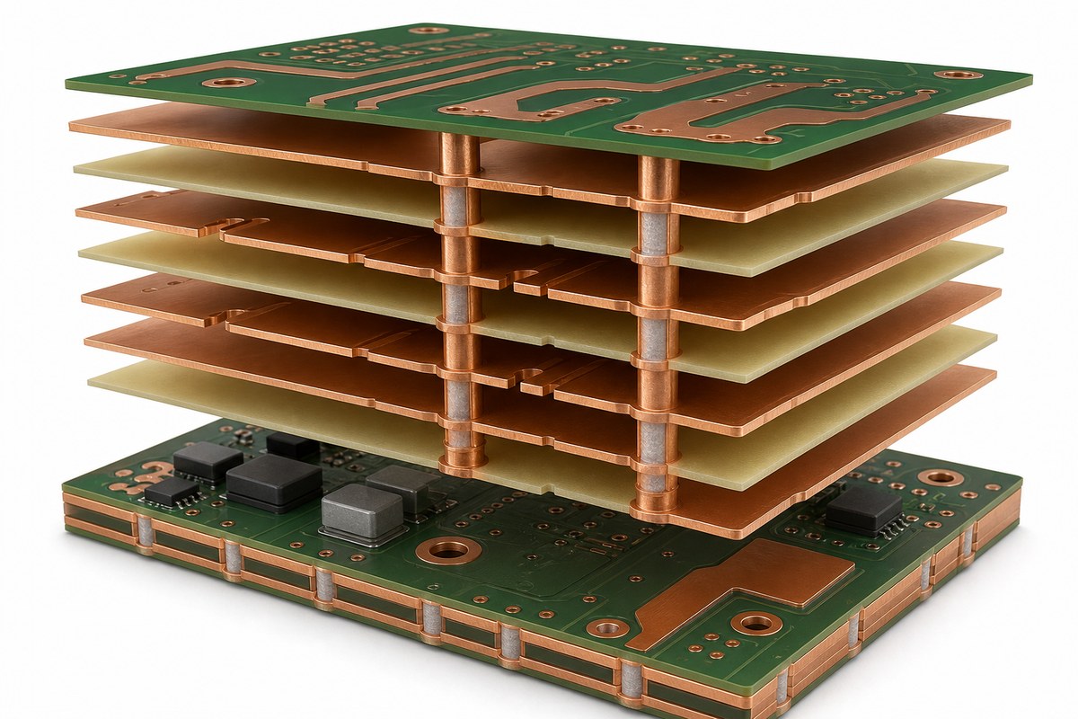
2 layer PCB stackup
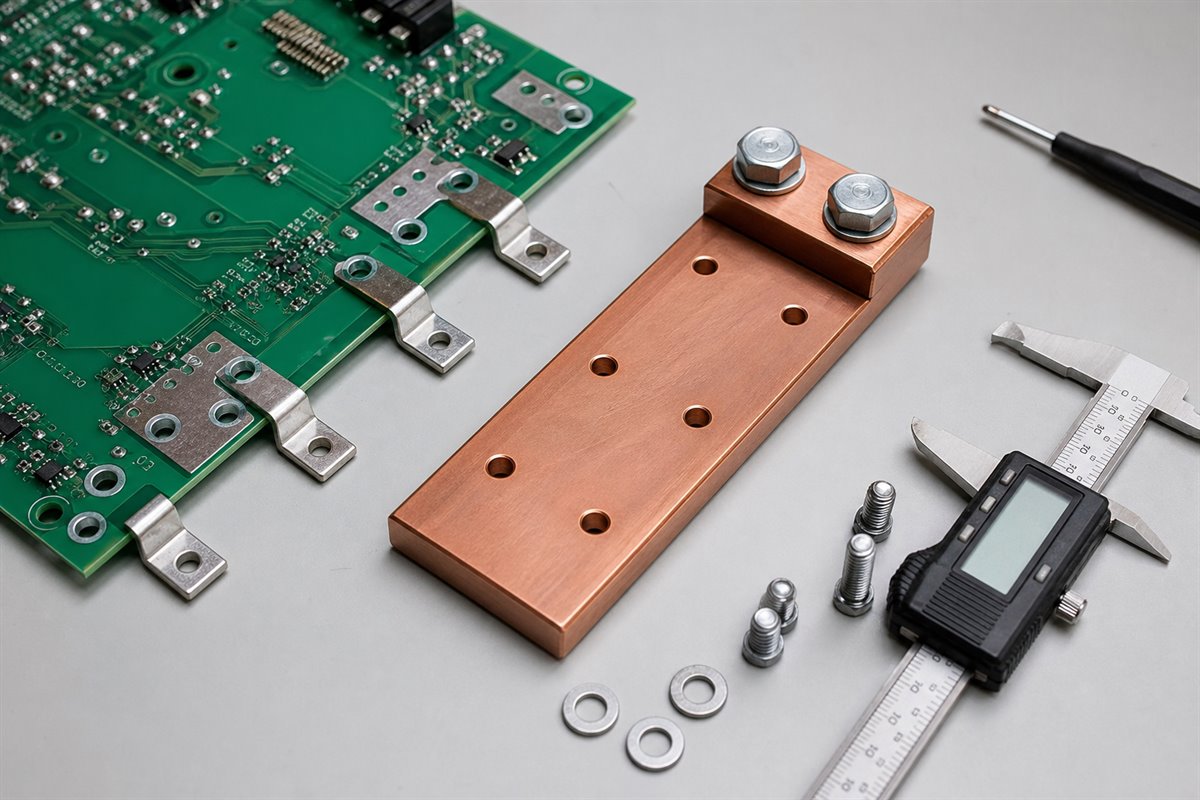
A 2 layer PCB stackup should be reviewed together with board thickness, copper weight, routing, and assembly needs.

What Is a 2 Layer PCB Stackup?

A 2 layer PCB stackup is the layer structure of a printed circuit board with one copper layer on the top side and one copper layer on the bottom side. Between the copper layers, the board normally uses an insulating core material such as FR4. Solder mask, silkscreen, and surface finish are then added according to the production requirement.

In everyday quoting, buyers may also call this a double sided PCB, two layer PCB, or 2 layer circuit board. These terms are closely related, but the stackup is the part that tells the manufacturer how the board thickness, copper, dielectric material, and layer arrangement should be built.

A useful 2 layer PCB stackup should make these points clear:

  • finished board thickness, such as 1.6 mm +/-10%;
  • top and bottom copper weight, such as 1 oz or 2 oz;
  • FR4 grade, high-Tg material, or other laminate requirement;
  • surface finish, such as HASL, lead-free HASL, ENIG, OSP, or immersion silver;
  • solder mask color and silkscreen requirement;
  • controlled impedance or special routing notes, if required;
  • SMT, through-hole, panelization, and test requirements.

Standard 2 Layer PCB Stackup Structure

A standard 2 layer PCB stackup is usually built with copper on both sides of an FR4 PCB core. The top layer may carry components, signals, power traces, and local ground copper. The bottom layer may provide additional routing, ground return paths, power routing, and connector connections.

2 layer PCB stackup
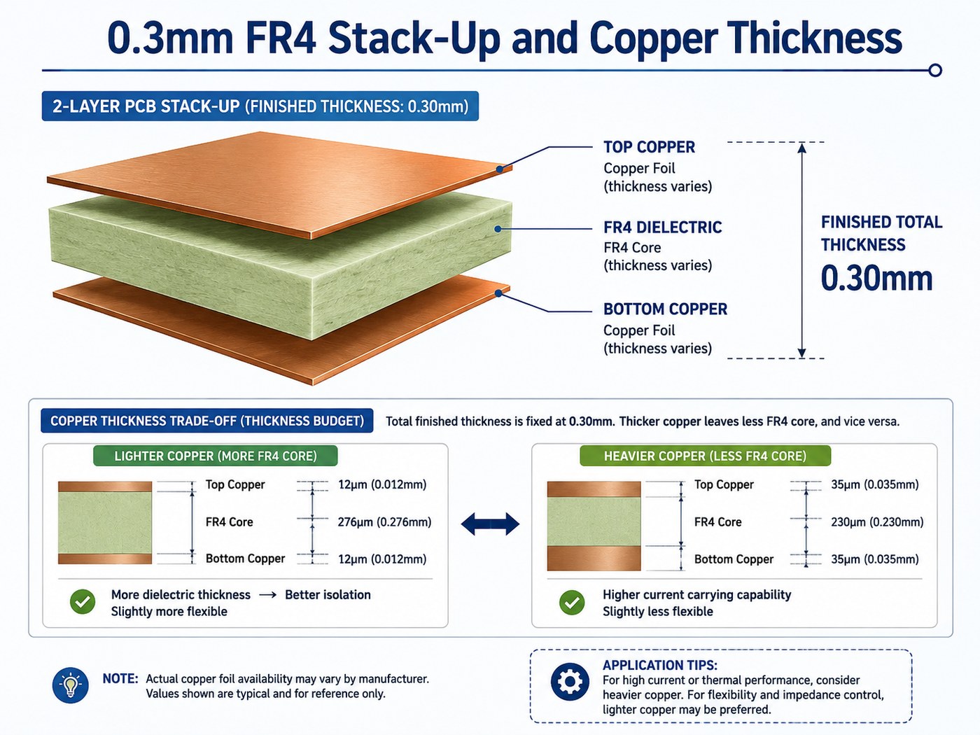
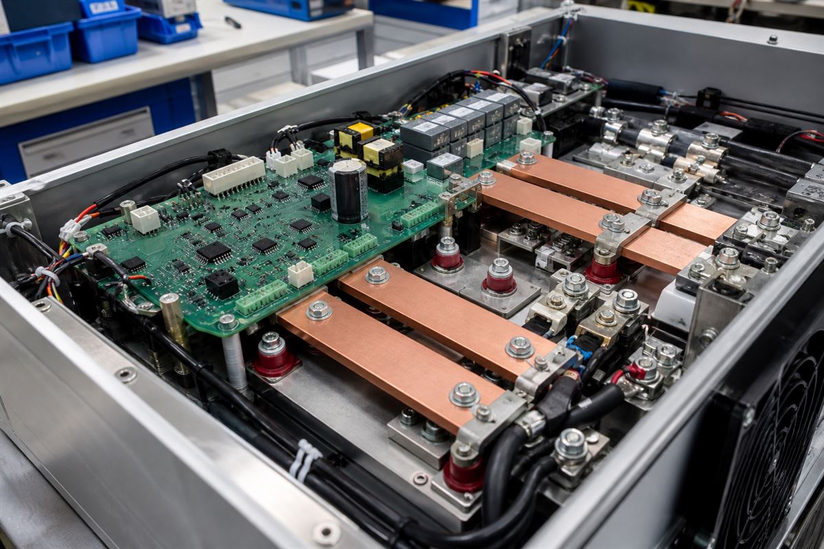
A 2 layer PCB usually includes top copper, an FR4 core, and bottom copper, with solder mask and surface finish added during production.
LayerPractical Role
Top solder maskProtects copper and defines solderable openings
Top copperComponents, signals, power, or ground copper
FR4 coreInsulation and mechanical support
Bottom copperRouting, return paths, connectors, or ground copper
Bottom solder maskCopper protection and solder control

The stackup may be simple, but the production result still depends on material availability, copper thickness, finished board thickness, drilling, solder mask registration, surface finish, and panelization. A two layer board should not be treated as a board with no engineering risk.

1.6mm 2 Layer PCB Stackup and Copper Weight

Many 2 layer PCB projects use a 1.6 mm finished board thickness because it is widely supported, mechanically stable, and compatible with many connectors and enclosures. However, 1.6 mm should refer to the finished board thickness, not only the raw laminate thickness.

2 layer PCB stackup
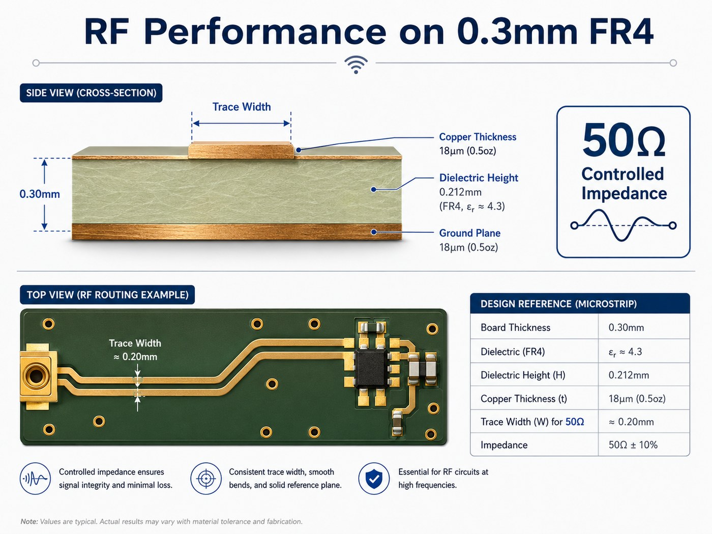
Finished board thickness is measured from the top surface to the bottom surface; copper weight is a separate specification.

Copper weight is a different requirement. For example, 1 oz copper describes the copper thickness or copper weight used on the conductive layers. It does not mean the whole board is 1 oz thick. This distinction matters when a drawing includes both board thickness and copper thickness.

Before production, confirm these thickness-related details:

  • finished board thickness and tolerance;
  • top and bottom copper weight;
  • whether copper is base copper or finished copper;
  • surface finish requirement;
  • connector or enclosure thickness limits;
  • whether impedance or current capacity depends on the stackup.

2 Layer PCB Stackup for Signal, Power, and Ground Routing

A 2 layer PCB gives less routing freedom than a 4 layer board, so the signal, power, and ground strategy must be practical. If the board has simple low-speed signals, connectors, LEDs, sensors, or basic control circuits, a two layer structure may be enough. If the board has high-speed interfaces, dense BGAs, strict EMI requirements, or multiple power domains, the project may need more review.

2 layer PCB stackup
Signal, power, and ground routing should be planned early on a 2 layer PCB because routing space is limited.

For many 2 layer boards, production review focuses on:

  • return path continuity for important signals;
  • wide enough power traces for current paths;
  • clear ground copper and via stitching where needed;
  • connector orientation and pin mapping;
  • thermal relief, copper balance, and solderability;
  • test points and inspection access after assembly.

The PCB manufacturer should not change the customer’s circuit intent. EBest Circuit can review whether the approved files are manufacturable and whether the stackup, copper, drilling, solder mask, and assembly notes are clear enough before production.

2 Layer PCB Stackup vs 4 Layer PCB Stackup

A 2 layer PCB stackup is often a good choice when the project needs a lower-cost board, simple routing, fast prototype validation, or a compact control board without strict high-speed requirements. A 4 layer stackup is usually considered when the board needs better power distribution, cleaner ground reference, controlled impedance, denser routing, or improved EMI behavior.

Item2 Layer PCB4 Layer PCB
Layer structureTop and bottom copperTwo outer layers plus inner planes
Routing spaceLimited but cost-effectiveMore routing freedom
Ground referenceDepends on copper planningUsually stronger with inner plane
CostLowerHigher
Best fitSimple to moderate circuitsDense, faster, or noise-sensitive boards

The right choice depends on the product, not only the layer count. If the 2 layer board can meet routing, grounding, thermal, and assembly needs, it may be the better commercial choice. If the board is already crowded or unstable, moving to 4 layers may save debugging time later.

Manufacturing Checks Before 2 Layer PCB Fabrication

A 2 layer PCB may be easier to manufacture than a high-layer-count board, but file review still matters. A small missing note can lead to wrong thickness, wrong surface finish, solder mask mismatch, connector fit problems, or assembly delay.

EBest Circuit typically checks:

  • Gerber or ODB++ file completeness;
  • drill file and plated-through-hole requirements;
  • finished board thickness and tolerance;
  • copper weight and current-related traces;
  • minimum line width, spacing, annular ring, and solder mask opening;
  • surface finish and solderability requirement;
  • panelization, tooling holes, fiducials, and breakaway method;
  • test requirement and outgoing inspection notes.

This review is useful because the buyer receives a finished PCB, not a file screenshot. The file must be translated into a real board that can be drilled, plated, etched, solder-masked, finished, tested, packed, and assembled.

SMT and PCBA Risks on 2 Layer PCB Boards

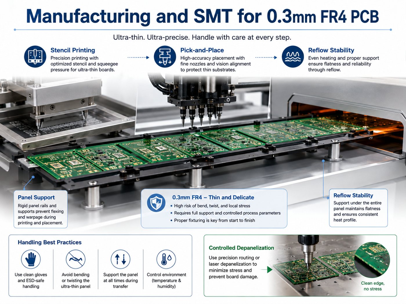
If the 2 layer PCB also needs SMT assembly, the stackup should be reviewed together with assembly data. Board thickness, panel size, component placement, solder mask openings, fiducials, and connector positions can all affect SMT yield. If the project also includes component sourcing, the BOM should be checked before SMT scheduling.

Before assembly, the useful files include:

  • Gerber or ODB++ files;
  • BOM with approved part numbers;
  • CPL or pick-and-place file;
  • assembly drawing;
  • polarity and orientation notes;
  • panelization drawing;
  • testing and packing requirements.

For prototype and small-batch PCBA projects, EBest Circuit can review PCB fabrication and SMT assembly together. This helps keep board thickness, panelization, component sourcing, soldering, inspection, and packing notes visible under one workflow. This is especially useful when the project is still in prototype PCB assembly validation.

EBest Circuit 2 Layer PCB Stackup Manufacturing Capabilities

EBest Circuit supports 2 layer FR4 PCB projects from prototype to small-batch and production runs. The practical value is not only making a bare board, but helping the customer confirm the production path before the order moves forward.

RequirementEBest Circuit Support
Board type2 layer FR4 PCB and double sided PCB
Thickness reviewFinished thickness and tolerance confirmation
Copper optionsCommon 1 oz or higher copper review by project
Surface finishHASL, lead-free HASL, ENIG, OSP, and other options
AssemblySMT, through-hole, mixed assembly, and inspection
DocumentsDFM notes, stackup confirmation, test reports when required

EBest Circuit (Best Technology) has worked in PCB and PCBA manufacturing since 2006 and serves customers in more than 40 countries and regions. For customers comparing suppliers, stable engineering communication is often as important as the quote itself, especially when the project needs both PCB fabrication and assembly.

2 Layer PCB Stackup Case Study for a Prototype Build

A USA customer needed a small-batch 2 layer PCB prototype for a compact control board. The board looked simple at first, but the project still had several details that could affect assembly and validation.

Project snapshot:

  • Customer region: USA;
  • Application: compact control and sensor interface board;
  • Quantity: 50 pcs prototype build;
  • PCB type: 2 layer FR4 PCB;
  • Finished thickness: 1.6 mm +/-10%;
  • Copper: 1 oz top and bottom copper;
  • Surface finish: lead-free HASL;
  • Assembly: SMT after PCB fabrication;
  • Delivery focus: prototype validation before the next small batch.
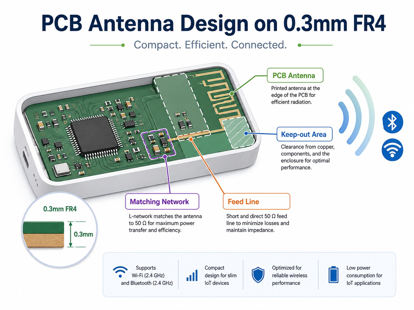
What EBest Circuit reviewed before production:

  • stackup, copper weight, board thickness, and solder mask notes;
  • panelization method for SMT handling;
  • BOM availability and approved part numbers;
  • component polarity, connector direction, and placement data;
  • electrical test before assembly and visual inspection after SMT;
  • single-board packing after assembly to reduce handling damage.

The useful result for the customer was a clearer prototype path. The order quantity was small, but the board still moved through file review, PCB fabrication, SMT preparation, inspection, and packing as one controlled project. That is the kind of support that helps engineering teams validate a 2 layer PCB before scaling the design.

FAQs About 2 Layer PCB Stackup

1. Is a 2 layer PCB stackup the same as a double sided PCB?
In most PCB manufacturing contexts, yes. A double sided PCB usually means a 2 layer PCB with copper on both the top and bottom sides.

2. What is the standard thickness for a 2 layer PCB?
Many 2 layer FR4 boards use 1.6 mm finished thickness, but 0.8 mm, 1.0 mm, 1.2 mm, and other thicknesses may also be used depending on the product.

3. Is 1 oz copper the same as 1.6 mm PCB thickness?
No. 1 oz copper describes the copper layer weight or thickness. 1.6 mm describes the finished board thickness from the top surface to the bottom surface.

4. Can a 2 layer PCB stackup support controlled impedance?
Some 2 layer boards can support impedance requirements, but the stackup, trace width, dielectric thickness, copper thickness, and test requirement should be reviewed before fabrication.

5. What files should I send for a 2 layer PCB quotation?
Send Gerber or ODB++ files, drill files, stackup or thickness notes, BOM, CPL, assembly drawing, surface finish requirement, quantity, test notes, and packing requirements.

All in all, a 2 layer PCB stackup should be clear before production begins. If your project needs 2 layer FR4 PCB fabrication, thickness review, copper confirmation, SMT assembly, or prototype-to-small-batch support, please send your Gerber files, BOM, CPL, drawings, and project notes to sales@bestpcbs.com. EBest Circuit can help review the manufacturing and assembly path before your boards move into production.

You may also like

Static Transfer Switch: PCB Risks OEMs Should Control

August 6th, 2026

A static transfer switch can move a critical load between two AC power sources fast enough to avoid an unacceptable interruption. For the OEM building that equipment, however, fast transfer depends on more than a switching specification. The sensing, control, gate-driver, power-supply, communication, and protection circuits must also be manufactured from the correct files and components.

If those PCB assemblies are quoted from incomplete information, the project can lose time through material substitutions, high-voltage spacing questions, thermal changes, connector mismatches, or an inspection plan that arrives too late. EBest Circuit (Best Technology) supports released-design PCB manufacturability review, PCB fabrication, BOM sourcing, SMT and through-hole assembly, and agreed testing assistance. Send your fabrication files, BOM, assembly data, and test requirements to sales@bestpcbs.com for a project-specific review.

static transfer switch
Control, sensing, gate-driver, and auxiliary-power PCBAs must match the released static transfer switch design.

What Does a Static Transfer Switch Do?

A static transfer switch monitors two available AC sources and transfers the connected load when the preferred source no longer meets the system’s defined conditions. Unlike a mechanically operated transfer device, the power path normally uses solid-state switching devices such as SCRs or thyristors. The exact transfer conditions, sequence, and timing depend on the released product design.

For an OEM, the practical benefit is continuity for a sensitive load. The manufacturing implication is that several electronic functions must work together:

  • source-voltage and frequency sensing;
  • synchronization or phase-related measurement, when required by the design;
  • decision and protection logic;
  • isolated gate-drive control;
  • auxiliary power conversion;
  • status indication, alarms, and communications;
  • temperature monitoring and cooling control.

These functions may be divided among several PCBAs or combined differently in each product. A PCB supplier should therefore manufacture the customer’s released architecture, not assume that every static switch uses the same board set.

The customer remains responsible for the STS topology, sensing thresholds, transfer logic, component selection, firmware, safety analysis, and final equipment validation. The PCB/PCBA manufacturer can check whether the released board data is manufacturable and whether the quoted build matches that data.

How Does STS vs ATS Change the Electronics You Need to Build?

The useful question in an STS vs ATS comparison is not simply which device is faster. It is which electronic scope the OEM must release, source, assemble, and test.

An ATS commonly depends on mechanical switching elements, while an STS uses solid-state power devices and electronic sensing and control. This difference can increase the amount of circuitry associated with gate drive, isolation, signal conditioning, auxiliary power, protection, and thermal monitoring. It can also create different PCB spacing, copper, component, and test requirements.

Do not turn the comparison into a universal timing promise. Transfer performance depends on source conditions, load characteristics, control strategy, device ratings, and the completed equipment. Instead, use the comparison to define the manufacturing package:

  • Which PCBAs belong to the static transfer switch?
  • Which high-voltage and low-voltage domains appear on each board?
  • Which components are safety-critical or substitution-controlled?
  • Which firmware is needed before functional testing?
  • Which tests can be completed at board level, and which require the full system?

This distinction prevents a supplier from treating an STS control board as an ordinary low-voltage controller and quoting only from board dimensions and layer count.

static transfer switch
Clear board part numbers, BOMs, and assembly drawings help suppliers quote the same STS manufacturing scope.

Which PCB Assemblies Matter Most in a Static Transfer Switch?

Knowing the board-level scope helps purchasing teams compare equivalent quotations and helps engineers avoid missing interfaces. Depending on the released architecture, a static transfer switch may include:

  • Control PCBA. Processes measurements, executes customer-developed logic, manages alarms, and coordinates the commanded transfer.
  • Sensing PCBA. Conditions voltage, current, frequency, phase, temperature, or status signals for the controller.
  • Gate-driver PCBA. Provides the isolation, pulse control, and interfaces required by the selected power-switching devices.
  • Auxiliary power-supply PCBA. Produces the regulated rails needed by the controller, sensors, drivers, relays, displays, and communications.
  • Interface or communication PCBA. Supports indicators, controls, network interfaces, or remote monitoring defined by the product.
  • Protection or interconnection board. Carries customer-defined protection components, connectors, terminal interfaces, or distribution paths.

Not every design separates these functions. The RFQ should use the actual board part numbers and revisions rather than a generic label such as “STS boards.” That gives the supplier a clear deliverable and prevents one quotation from including three PCBAs while another includes five.

For each PCBA, identify whether the order covers bare PCB fabrication, customer-supplied components, full BOM sourcing, assembly, programming, conformal coating, inspection, or testing assistance. Clear scope produces a quotation that purchasing can use instead of a low initial price followed by additions.

Which Manufacturing Risks Can Delay an STS Build?

Most avoidable delays begin before assembly. The supplier receives enough information to calculate a price, but not enough to confirm that the board can be built and accepted.

Release these risk items before material is purchased:

  • Unclear high-voltage boundaries. The fabrication data may not show the voltage domains, required spacing, slotting, barriers, or customer-approved constraints.
  • Late stack-up changes. A changed dielectric construction can affect finished thickness, copper geometry, controlled impedance, isolation features, and mechanical fit.
  • Heavy-copper or current-path assumptions. Copper weight alone does not define current capacity or thermal performance. The approved layout, copper construction, temperature limits, and system cooling remain essential.
  • Mixed component technologies. Large terminals, transformers, relays, heat-sensitive parts, fine-pitch devices, and through-hole power components may require different assembly controls.
  • Uncontrolled substitutions. A component that looks electrically similar may differ in package, isolation rating, thermal behavior, qualification status, or firmware compatibility.
  • Incomplete test access. Important nodes may be inaccessible after assembly, while the required fixture or firmware has not been released.
  • Mechanical interface errors. Connector height, orientation, mounting holes, heat-sink interfaces, and enclosure clearances can stop final integration even when the PCBA passes electrical inspection.

A manufacturability review can identify conflicts between the released files and the intended fabrication or assembly process. It does not replace the customer’s electrical, thermal, mechanical, or safety design decisions.

What Should You Confirm Before Ordering Static Switch PCBAs?

Before ordering static switch PCBAs, make the approved requirement visible in the fabrication drawing, assembly drawing, BOM notes, purchase order, and test specification. A requirement mentioned only in an email is easy to miss during sourcing or production.

Confirm the following before the purchase order:

  • current PCB and PCBA part numbers with revision status;
  • complete Gerber or ODB++ data, drill files, drawings, and stack-up;
  • finished board thickness, copper construction, surface finish, solder mask, and marking requirements;
  • voltage domains and customer-specified spacing, slots, barriers, or isolation requirements;
  • exact connector, terminal, transformer, optocoupler, driver, controller, and power-device part numbers;
  • do-not-substitute items and the approval route for alternatives;
  • polarity, orientation, torque, heat-sink, insulation, and mechanical-interface notes;
  • programming files, version control, and device-programming instructions;
  • inspection standard, acceptance class, sample plan, and required records;
  • test procedure, fixture responsibility, limits, and report format.

If any requirement is still pending, identify it as pending. That is safer than allowing each supplier to build a different assumption into the quote.

How Can BOM Sourcing Prevent SCR and Driver-Component Delays?

Critical components can hold up the entire build even when the PCBs are ready. The buyer benefits when availability and substitution rules are checked before the order is released, not after assembly is scheduled.

The BOM should provide the manufacturer part number, description, package, quantity, approved alternatives, and substitution authority for every line. Pay particular attention to:

  • SCRs, thyristors, IGBTs, or other customer-selected switching devices;
  • isolated gate drivers and optocouplers;
  • voltage and current sensing components;
  • microcontrollers, DSPs, programmable logic, and memory;
  • isolation transformers and auxiliary power modules;
  • safety-rated capacitors, resistors, fuses, and protection devices;
  • connectors, terminal blocks, relays, and mechanically constrained parts.

For components mounted outside the PCBA, clarify whether they are included in the sourcing scope. A switching module shown on a system drawing may not appear on the assembly BOM, yet purchasing may still expect the PCBA supplier to provide it.

EBest Circuit can source components against a customer-released BOM and raise availability or substitution questions for approval. The customer retains responsibility for selecting the components and approving any alternative that could affect electrical performance, isolation, thermal behavior, compliance, or firmware.

static transfer switch
Inspection and functional-test evidence should follow the customer-approved procedure and acceptance limits.

What Inspection and Testing Evidence Should an STS Order Include?

Inspection records help the customer decide whether the delivered PCBAs match the released order. They should be defined before production so that the supplier can price the necessary work and preserve the required evidence.

Match each record to a real acceptance decision:

  • material and stack-up confirmation for the bare PCB;
  • certificate of conformance when required;
  • solder paste inspection and automated optical inspection records where applicable;
  • X-ray inspection for hidden joints or selected power and BGA components when specified;
  • polarity, orientation, workmanship, and through-hole solder inspection;
  • dimensional, connector-position, or mechanical-interface checks;
  • programming verification and firmware-version record;
  • electrical or functional test results based on customer-provided limits;
  • nonconformance, repair, and deviation records;
  • serial-number or lot traceability when required.

Board-level testing cannot prove the completed STS will meet its transfer-time, load, fault, thermal, EMC, safety, or reliability requirements. Those are system-level acceptance responsibilities unless a separately defined and authorized test scope says otherwise.

When EBest Circuit assists with functional testing, the RFQ should identify the customer-provided fixture, software, firmware, operating instructions, safe power conditions, expected readings, pass/fail limits, and report format. This turns “function test required” into a test that can actually be quoted and repeated.

Which Files Produce a More Accurate Static Transfer Switch Quote?

An accurate static transfer switch PCBA quote starts with a package that lets the supplier understand what must be delivered. Sending only Gerber files may produce a bare-board price, but it cannot define sourcing, assembly, programming, inspection, or test scope.

Send one controlled RFQ package containing:

  • PCB fabrication data and fabrication drawing;
  • approved stack-up or construction requirements;
  • assembly drawings for top and bottom sides;
  • complete BOM with approved manufacturers and substitution rules;
  • centroid or pick-and-place data;
  • schematic for engineering reference when permitted;
  • polarity, orientation, connector, and mechanical-interface notes;
  • programming files and instructions;
  • workmanship and acceptance requirements;
  • inspection and test specifications;
  • prototype quantity, expected production quantity, and delivery target;
  • required reports, traceability, labeling, and packaging instructions.

Ask the supplier to list assumptions, exclusions, separately priced options, and unresolved engineering questions. This makes quotations easier to compare because each supplier is pricing the same manufacturing outcome.

How Can One PCB and PCBA Supplier Reduce STS Production Handoffs?

Using one supplier for PCB fabrication, BOM sourcing, assembly, and agreed testing assistance can reduce the number of handoffs the OEM must coordinate. The benefit is not simply fewer purchase orders. It is a clearer path from the released PCB construction to the assembled and documented PCBA.

EBest Circuit can support:

  • PCB layout manufacturability review against the released requirements;
  • prototype and production PCB fabrication;
  • BOM sourcing with customer-controlled substitutions;
  • SMT and through-hole assembly;
  • inspection, programming, and agreed test assistance;
  • production records and traceability defined in the order.

This combined scope is useful when a static transfer switch contains several related board assemblies with shared components, connectors, revisions, or inspection requirements. Engineering questions can be raised before fabrication or material purchasing rather than being discovered during final assembly.

The boundary remains important: EBest Circuit does not take ownership of the STS electrical architecture, transfer algorithm, firmware validation, product certification, or final equipment safety unless a separate written scope explicitly defines an authorized activity. We manufacture and assemble to the customer’s released and approved requirements.

FAQs About Static Transfer Switch PCB Manufacturing

Is a static transfer switch the same as an automatic transfer switch?
No. An STS normally uses solid-state switching devices, while an ATS commonly uses mechanical switching elements. The resulting transfer behavior and electronic manufacturing scope can differ. The product designer must determine which architecture suits the application.

Can a PCB supplier select the SCR or thyristor for an STS?
The system designer should select and approve the power-switching device based on the electrical, thermal, fault, control, safety, and qualification requirements. A sourcing supplier can check availability and propose alternatives for customer review, but should not silently replace the approved device.

Does PCBA functional testing prove the complete STS will transfer correctly?
Not by itself. A board-level test can verify specified inputs, outputs, programming, or communication functions. Complete transfer performance depends on the assembled system, sources, load, firmware, switching devices, sensing, cooling, protection, and customer-defined operating conditions.

What should be marked as do not substitute in the BOM?
Mark any component whose replacement could affect electrical performance, isolation, safety, thermal behavior, mechanical fit, programming, qualification, or regulatory evidence. Also state who may approve an alternative and what evidence is required.

Can EBest Circuit manufacture all PCBAs used in a static transfer switch?
EBest Circuit can review and quote released PCB/PCBA packages that fit its manufacturing, sourcing, assembly, and agreed testing capabilities. Feasibility depends on the board construction, components, assembly process, inspection needs, quantities, and test scope. Send the current files to sales@bestpcbs.com for review.

Before releasing your next static transfer switch prototype or production order, confirm the board list, revision, BOM controls, manufacturing requirements, and acceptance evidence. A complete package helps EBest Circuit return a more usable quotation and identify manufacturability or sourcing questions before they become schedule delays.

You may also like

Microcontroller Industrial Guide for Reliable Control Board Design

August 6th, 2026

A microcontroller industrial design uses an MCU as the real-time control core of equipment that must operate around electrical noise, field wiring, temperature variation, vibration, long service cycles, and repeat production. The chip matters, but the complete controller also needs protected power, conditioned I/O, suitable communication, reliable firmware, a manufacturable PCB, and a test plan.

This guide explains how engineers can select an industrial MCU and turn it into a production-ready control board. It also draws a practical boundary between a custom MCU board and a PLC, so teams do not choose a low-cost chip and then underestimate the work needed to make the surrounding system reliable.

Microcontroller industrial control PCB with protected field I/O and Ethernet

What Does “Microcontroller Industrial” Mean?

“Microcontroller industrial” describes the use of an MCU in industrial equipment, not a universal chip category with one fixed specification. A microcontroller combines a processor core, program memory, data memory, timers, communication peripherals, and configurable I/O in one integrated circuit.

In an industrial product, that MCU may read sensors, run control loops, generate PWM, manage alarms, communicate with a supervisory system, and place outputs into a safe state after a fault. The device must be selected for the actual electrical and environmental requirements, while the surrounding PCB supplies the protection and interfaces that the chip does not provide by itself.

For a broader explanation of the component and its assembly requirements, see our microcontroller unit PCB assembly guide.

What Makes a Microcontroller Industrial Grade?

A microcontroller industrial grade choice is one whose exact orderable part, package, temperature rating, lifecycle status, safety resources, and peripherals match the target equipment. The phrase “industrial grade” alone is not enough evidence.

Check the manufacturer datasheet and ordering information for:

  • Operating temperature: verify the rated junction or ambient range for the exact suffix, not only the MCU family page.
  • Supply supervision: brownout reset, power-on reset, watchdogs, clock monitoring, and error flags help the system respond to abnormal conditions.
  • Memory integrity: error detection, ECC, CRC support, and documented retention or endurance may matter in long-life equipment.
  • Peripheral fit: timers, PWM, ADCs, comparators, CAN, Ethernet, UART, SPI, and I2C must cover the real I/O plan without exhausting resources.
  • Safety and security support: some MCU portfolios provide safety manuals, FMEDA data, diagnostic libraries, secure boot, or hardware security features for specific products.
  • Availability: confirm product status, approved alternates, package supply, and the manufacturer’s longevity commitment before freezing the design.

The board still needs external transient protection, isolation, filtering, power conversion, and thermal design. A wide-temperature MCU on an unprotected PCB is not automatically an industrial controller.

Which MCU Architecture and Peripherals Fit the Application?

The best MCU is the least complex device that satisfies the timing, memory, peripheral, safety, software, and lifecycle requirements with practical margin. Core frequency alone is a poor selection method.

Requirement MCU Feature to Check Typical Industrial Use
Simple sequencing and monitoring GPIO, timers, ADC, watchdog Sensor node, relay controller, small actuator
Motor or power control High-resolution PWM, fast ADC, comparators, control accelerator Drive, inverter, power converter, pump controller
Connected control CAN, Ethernet MAC, multiple serial interfaces, security Gateway, remote I/O, machine controller
Safety-related function Safety documentation, diagnostics, memory protection, independent watchdog Monitored shutdown, safety co-processor, protected actuator
High data or graphics load More RAM, external-memory interface, DMA, display or camera support HMI, vision-assisted controller, data acquisition

Build a peripheral budget before choosing the package. Count ADC channels, timer channels, communication ports, DMA requests, interrupt sources, programming pins, oscillator pins, and spare I/O. Then check whether those functions can be used simultaneously on the selected pinout.

Microcontroller Industrial Applications

Microcontroller industrial applications are strongest where a product needs compact embedded control, repeatable timing, custom interfaces, and scalable unit cost. Common examples include:

  • motor drives, pumps, fans, compressors, and positioning systems;
  • sensor transmitters, condition-monitoring nodes, and data loggers;
  • remote I/O modules, compact machine controllers, and protocol gateways;
  • power supplies, inverters, battery-related controls, and energy meters;
  • valve controllers, dosing equipment, thermal controllers, and laboratory instruments;
  • human-machine interface panels and embedded diagnostic modules.

The MCU should be selected from the load and environment backward. A motor-control board may prioritize synchronized PWM and fast current sampling, while an industrial sensor node may prioritize low-noise analog acquisition, low power, secure communication, and stable calibration storage.

Microcontroller for Industrial Automation: When Is It a Better Fit Than a PLC?

A microcontroller for industrial automation is a better fit when the controller is embedded inside a repeatable product and the manufacturer can own the hardware, firmware, compliance, and lifecycle work. A PLC is usually better when users need modular field I/O, standardized programming, fast cabinet integration, and maintenance by plant technicians.

Option Best Fit Main Trade-Off
Custom MCU board High-volume or space-constrained product with fixed functions Requires custom protection, firmware, validation, and lifecycle ownership
Industrial controller module Embedded product needing prebuilt I/O or communication Higher module cost and less hardware freedom
PLC Machine or process automation maintained on the factory floor Larger size and higher unit cost, but faster integration and service

Some systems use both: an MCU controls a dedicated product or subsystem, while a PLC coordinates the machine. The right comparison is total engineering and lifecycle cost, not chip price versus PLC purchase price.

How Do Power, I/O Protection, and Isolation Prevent Failures?

Power conditioning, field-I/O protection, and isolation prevent predictable electrical stress from reaching the MCU. They must be designed around the real supply, cable length, load type, grounding system, and applicable immunity requirements.

  • Power entry: define reverse-polarity, overcurrent, surge, transient, undervoltage, and inrush behavior before selecting regulators.
  • Digital inputs: use current limiting, filtering, threshold control, and isolation where field voltage or ground offset requires it.
  • Analog inputs: protect against overvoltage while controlling leakage, bandwidth, source impedance, and ADC settling error.
  • Outputs: select drivers and clamps for the real relay, valve, solenoid, lamp, or motor load, including inductive energy.
  • Communication ports: coordinate the transceiver, termination, common-mode range, ESD path, shield connection, and isolation strategy.

Protection parts work only when the PCB gives fault current a short, controlled path. Poor component placement or a long return trace can reduce the value of a correctly selected suppressor.

Industrial MCU PCB with separated protected power and field I/O sections

Which Industrial Communication Interfaces Matter?

The right industrial interface is the one required by the connected equipment, distance, timing, topology, and noise environment. The MCU peripheral is only one part of that interface.

  • UART, SPI, and I2C: useful for short on-board links to sensors, memories, displays, and companion ICs.
  • RS-485: practical for differential multidrop links, but the complete design must address termination, bias, grounding, and protocol timing.
  • CAN: useful for robust multi-node control and diagnostics when the transceiver, termination, and message strategy are correctly designed.
  • Ethernet: supports higher data rates and network integration, while adding magnetics, impedance, clock, connector, surge, and software requirements.
  • Industrial Ethernet or fieldbus: may require dedicated controllers, licensed stacks, conformance testing, or a companion communication device.

Do not select an MCU because its feature list says “Ethernet” or “CAN” without checking the physical layer, software stack, certification path, and available CPU and memory after the application is running.

How Should an Industrial Microcontroller Board Be Designed?

An industrial microcontroller board should be partitioned by power level, noise source, signal sensitivity, isolation domain, and current-return path before detailed routing starts. Placement makes the protection and EMC strategy visible.

Useful board-level practices include:

  • place decoupling capacitors at MCU supply pins with compact current loops;
  • keep crystal and clock paths short and away from switching nodes;
  • separate field connectors and protection components from low-voltage logic;
  • route high-current and fast-switching loops before sensitive analog signals;
  • maintain application-appropriate creepage, clearance, and isolation gaps;
  • give Ethernet, USB, or other controlled-impedance routes a continuous reference plane;
  • provide programming, reset, rail, communication, and critical-I/O test access;
  • review connector retention, mounting holes, enclosure clearances, and service access.

Our custom PCB design for industrial use guide expands on enclosure, power, field wiring, and I/O planning.

Industrial microcontroller control board installed in a factory automation enclosure

How Should Firmware, Watchdogs, and Functional Safety Be Planned?

Firmware reliability starts with defined fault responses, not with a watchdog added at the end. The hardware and software teams should agree on safe outputs, reset behavior, diagnostic coverage, update control, and recovery before board release.

  • initialize outputs to a safe state before normal control begins;
  • use brownout, clock, memory, and watchdog diagnostics where appropriate;
  • verify that the watchdog is serviced by healthy task execution, not an unconditional loop;
  • protect boot and update paths against incomplete or unauthorized firmware;
  • record firmware version, configuration, and calibration data for traceability;
  • separate independent shutdown hardware from normal software control when the risk analysis requires it.

IEC 61508 or another functional-safety standard applies at the system level, not merely because an MCU family offers safety documentation. Use the exact device safety manual and FMEDA package when the product’s hazard analysis calls for them, and verify the complete hardware, software, development, and validation process.

How Should PCB Assembly and Test Access Be Prepared?

Assembly and test should be designed before the first production panel because MCU boards combine fine-pitch packages, sensitive clocks, programming access, mixed-voltage I/O, and firmware-dependent tests. A complete build package reduces revision mistakes and fixture delays.

Prepare and control:

  • Gerber or ODB++ data, drill files, stackup, fabrication drawing, and panel requirements;
  • BOM with manufacturer part numbers, approved alternates, and do-not-substitute items;
  • centroid data, assembly drawings, polarity information, and special handling notes;
  • programming image, tool, connector, version rule, checksum, and serialization method;
  • test-point map, fixture interface, input simulation, output loads, and pass/fail limits;
  • inspection requirements for fine-pitch, QFN, BGA, through-hole, and hidden solder joints.

The production workflow should connect fabrication, sourcing, assembly, programming, and test. Our PCB manufacturing and assembly guide explains those handoffs, while the PCBA programming guide covers customer-provided firmware and production access.

What Should Engineers Validate Before Production?

Engineers should validate the board against its real operating envelope, fault cases, communication load, firmware image, and production test method before releasing volume builds. Bench function at room temperature is only the starting point.

  1. Confirm every rail during startup, normal load, communication activity, and output switching.
  2. Exercise minimum and maximum input conditions, sensor faults, disconnected cables, and defined overload cases.
  3. Check reset, brownout, watchdog, clock-failure, and firmware-update recovery behavior.
  4. Review thermal hot spots inside the intended enclosure and mounting orientation.
  5. Run the applicable EMC, ESD, surge, electrical-fast-transient, vibration, and environmental tests for the end product.
  6. Verify programming time, test coverage, traceability data, and fixture repeatability on pilot units.
  7. Freeze the approved BOM, firmware, manufacturing data, and test limits under one revision.

A second microcontroller industrial review should happen after pilot production: compare the designed test coverage with actual assembly findings, programming logs, and field-risk assumptions before scaling.

Industrial microcontroller PCB validation with oscilloscope probes and test fixture

FAQ About Microcontroller for Industrial Automation

What microcontroller is used in industry?

Industry uses many MCU families from established semiconductor manufacturers. The correct device is chosen by real-time performance, memory, peripherals, temperature grade, safety and security resources, software ecosystem, package, availability, and cost rather than by one universal brand ranking.

What are industrial-grade microcontrollers?

Industrial-grade microcontrollers are exact MCU products rated and supported for specified industrial requirements, such as an extended operating-temperature range, long availability, robust diagnostics, or safety documentation. Verify the full part number and datasheet because ratings can differ within one family.

Is an STM32 microcontroller industrial grade?

Some STM32 devices and orderable variants target industrial applications, but “STM32” alone does not establish the temperature grade or safety support. Check the specific part number, package suffix, datasheet, product status, and required software or safety collateral.

Can ESP32 be used in industrial applications?

An ESP32-based design can be used in some industrial products if the exact device or module, temperature rating, RF requirements, lifecycle, security, power design, protection, enclosure, and compliance plan meet the application. A consumer development board should not be treated as a finished industrial controller.

Are microcontrollers used inside PLCs?

Many PLCs and industrial controllers use MCUs or processors internally, but the finished PLC adds protected I/O, power conditioning, communication, firmware, mechanical packaging, qualification, and a serviceable programming environment. The chip and the complete controller are not equivalent products.

What is the difference between a PLC and a microcontroller?

A microcontroller is an integrated circuit that must be designed into custom hardware, while a PLC is a finished industrial control platform with field I/O, power, enclosure, programming tools, and maintenance conventions. Custom MCU boards favor product integration; PLCs favor faster machine integration and field service.

Does an industrial MCU board need galvanic isolation?

Isolation is needed when the risk analysis identifies hazardous voltage, large ground-potential differences, noisy field wiring, or a required safety barrier. Not every interface needs isolation, and the barrier must include signal, power, creepage, clearance, and layout requirements.

Which communication protocol is best for an industrial MCU?

No protocol is best for every system. Choose according to distance, topology, data rate, determinism, interoperability, software stack, EMC environment, and conformance needs. RS-485, CAN, Ethernet, and application-specific industrial networks solve different problems.

What temperature range should an industrial microcontroller support?

The required range comes from the product’s measured internal temperature and specified operating environment. Select an exact MCU variant whose rated conditions cover that range with margin, then verify the board, components, enclosure, and thermal design under worst-case operation.

What files are needed to manufacture an industrial microcontroller board?

A complete package normally includes Gerber or ODB++ data, drill files, stackup and fabrication notes, BOM, centroid data, assembly drawings, programming files and instructions, test requirements, quantity, and approved revision information. Add enclosure, connector, coating, or traceability requirements when they affect production.

How Can EBest Circuit Support Your Industrial MCU Board?

At EBest Circuit, we support industrial control projects with PCB fabrication, component sourcing, SMT and through-hole assembly, inspection, customer-provided firmware programming, and test coordination. Our role is to connect the board data, BOM, assembly details, programming access, and acceptance criteria before production begins.

If your industrial MCU board is ready for review, send your Gerber or ODB++ files, BOM, centroid data, assembly drawing, firmware instructions, test requirements, quantity, and operating-environment notes to sales@bestpcbs.com. We will review the manufacturing and PCBA scope and identify the questions that should be resolved before quotation.

You may also like

What Is a Guard Ring PCB? How to Design It on a PCB Layout?

August 6th, 2026

A guard ring pcb uses a conductive trace around a high-impedance node to intercept surface leakage before it reaches the sensitive copper. The guard is most effective when a low-impedance source drives it close to the protected node’s voltage. It is not automatically a grounded shield, a board-edge ground ring, a via fence, or the annular copper around a drilled hole.

A successful layout starts with the circuit, not the shape. Identify the node whose allowable error is comparable to expected leakage, select a guard voltage that minimizes the voltage across unwanted surface paths, enclose the complete sensitive path, control contamination, and test the assembled prototype under realistic conditions.

Guard ring PCB on a precision electronics inspection bench

What Is a Guard Ring PCB?

A PCB guard ring is copper placed around a leakage-sensitive node and connected to a controlled low-impedance potential. Its job is to collect current that would otherwise cross the board surface into the protected input. The protected object may be an op-amp input pin, a photodiode node, a transimpedance feedback junction, an electrometer input, or another point where picoampere-level current can create a material error.

The word “ring” describes electrical enclosure, not necessarily a perfect circle. The copper may form an irregular closed trace around pads, a short route, and selected component terminals. Components that connect the sensitive node to lower-impedance circuitry often straddle the guard so the guarded copper does not extend beyond the enclosure.

Three similar-looking structures solve different problems. A driven guard reduces leakage into a high-impedance node. A grounded board-edge ring can support electromagnetic containment, while a PCB ground loop is an unwanted return-current path. An annular ring is the copper surrounding a drilled hole. Treating these features as interchangeable can create a layout that looks protected but does not control the intended current path.

How Does a Guard Ring Work on a PCB Layout?

A guard ring works by reducing the voltage that drives leakage toward the sensitive node and by providing that leakage with a lower-impedance destination. Surface current is governed by the voltage across an unintended resistance. For a simplified path, Ileak = (Vsource – Vnode) / Rsurface. This relationship is useful for estimating scale, not for assigning one fixed resistance to every board.

Suppose a nearby conductor is 5 V away from a sensitive input and the contaminated surface path is 100 Gohm. The simplified leakage is 50 pA. If a low-impedance guard reduces the voltage across the final path to 1 mV, the same assumed resistance would correspond to 10 fA. Real layouts contain several parallel surface and bulk paths, so this calculation is a design check rather than a guaranteed result.

The guard must remain low impedance across the relevant frequency range. A weak source can move when it collects leakage or coupled current. A long guard can also add capacitance to the sensitive network or load its driver. The circuit therefore needs both a suitable DC potential and adequate driver stability.

When Should You Use a Guard Ring in PCB Design?

Use a guard ring when board leakage can consume a meaningful part of the circuit’s error budget. The decision depends on source impedance, allowable input current, adjacent voltages, contamination exposure, humidity, temperature, and the input behavior of the selected device. A guard is common in low-current measurements, but it is not a universal upgrade for every analog trace.

  • Photodiode and transimpedance inputs: leakage entering the summing node can appear as false sensor current and create output offset.
  • Electrochemical and pH interfaces: high source impedance makes the input vulnerable to small surface currents and residue.
  • Precision op-amp inputs: a guard may be justified when PCB leakage is comparable to input bias current or the permitted offset-current error.
  • Multiplexer channels: off-channel voltage and package or board leakage may disturb a high-impedance selected channel.
  • Low-resistance signal paths: a driven guard is usually unnecessary when ordinary spacing, a continuous reference plane, and clean routing already keep leakage far below the error budget.

Do not use a driven guard as a substitute for fixing a broken return path, inadequate creepage, poor shielding, excessive sensitive-trace length, or an unsuitable component. High voltage safety spacing and RF isolation require their own analysis.

Should a PCB Guard Ring Connect to Ground or a Driven Voltage?

Connect the guard to the lowest-impedance node that closely follows the protected node’s operating voltage; use ground only when ground satisfies that condition. A grounded guard around a node that sits several volts above ground can increase the electric field across the remaining insulation and may create more leakage than a properly driven guard.

Circuit condition Guard connection to evaluate Main check
Protected node remains near ground Quiet, low-impedance ground Confirm ground noise and return current do not modulate the guard
Noninverting high-impedance input Low-impedance node that tracks the input, often selected from the amplifier topology Verify common-mode range, stability, and voltage tracking
Inverting or transimpedance summing node A low-impedance reference near the virtual-node potential Confirm the guard does not enclose or load the wrong net
Dedicated guard-output device Manufacturer-defined guard output Follow its routing, load-capacitance, and stability guidance

Choose the connection from the device data sheet and circuit configuration rather than copying a nearby layout. The correct net can change between inverting, noninverting, buffer, multiplexer, and electrometer circuits. Check the guard over the full input range, during power sequencing, and when the driver saturates or loses power.

How Should You Design a Guard Ring on a PCB Layout?

Design the guard to enclose every practical surface path into the sensitive node while keeping the protected copper short. Start at the package pin, follow the complete high-impedance net, and identify every pad, via, connector, test point, and component lead that can create a bypass around the guard.

  1. Define the protected net: mark the exact package pins, pads, vias, feedback junctions, connector contacts, and test features whose leakage allowance is limited. Extend the boundary only as far as the high-impedance condition exists. If a series component changes the node to a low-impedance signal, place that component at the boundary instead of guarding unnecessary downstream copper.
  2. Select the guard source: document the expected guard voltage, output impedance, operating range, startup state, and capacitive-load limit. Check the voltage difference between the guard and protected node at the minimum and maximum signal levels, not only at the nominal bias point. Also review power-up, shutdown, saturation, and disconnected-sensor conditions because the two nodes may temporarily separate.
  3. Shorten sensitive copper: place the input device and critical passive components before drawing the guard. Keep the guarded trace direct, minimize exposed pad area, and avoid optional test pads or long connector stubs inside the enclosure. The ring should protect a compact node; it should not be used to justify a longer high-impedance route.
  4. Enclose the surface path: route a continuous guard between the sensitive copper and nearby conductors that can drive leakage. Close practical gaps around pads and component bodies, but do not cut through required land patterns or assembly clearances. Resistors, capacitors, or other boundary components can straddle the guard when one terminal belongs to the protected node and the other belongs outside it.
  5. Review every layer: inspect the same XY area on the top, bottom, and internal layers. A top-layer ring cannot intercept contamination on the bottom surface, and an unrelated plane directly below can add capacitance or create a field across the laminate. For a through-hole input or a bottom-side sensitive path, evaluate guarding on both outer layers and keep unrelated copper away from the protected volume.
  6. Add guarded transitions deliberately: connect top and bottom guard copper with guard-net vias when both surfaces need the same controlled potential. Place enough connections to avoid isolated copper and excessive guard impedance, but do not copy RF via-fence spacing rules into a low-leakage circuit without an electrical reason. Keep ordinary ground, power, and signal vias outside the guarded boundary unless the schematic explicitly requires them there.
  7. Apply fabrication constraints: choose guard width, clearance, annular geometry, solder-mask treatment, and copper-to-pad spacing that the selected PCB process can reproduce and inspect. Put the guard net name, mask openings, controlled keepouts, and any unusual cleaning requirement into the fabrication and assembly data. Confirm that automated optical inspection, probing, rework access, and depanelization will not damage or contaminate the guarded area.
  8. Check parasitic effects: estimate guard-to-node capacitance, driver loading, settling time, and stability instead of assuming more copper is always better. A wide guard or large guard plane may improve interception yet increase capacitive load on the driver and coupling to the sensitive node. Review the amplifier or guard-driver guidance, then verify settling and oscillation behavior on the assembled prototype.

There is no universal guard width or clearance. The fabricator’s minimum feature rules establish what can be built, but they do not prove the electrical design. Voltage difference, contamination exposure, assembly residues, device guidance, guard-driver capability, and measured leakage determine whether the guard ring pcb geometry is adequate.

Before releasing Gerbers, perform a boundary walk from the sensitive pin around the complete enclosure. Confirm that no pad, via, plane edge, mask-defined opening, test point, or connector contact creates an unguarded shortcut. This final spatial review is especially important when schematic nets appear correct but library courtyards, plane pours, or bottom-side features have changed during layout.

How Should You Handle Solder Mask, Cleaning, and Conformal Coating Around a Guard Ring?

Treat solder mask, cleanliness, and coating as electrical design variables because each one can change the leakage path around the guarded node. The production drawing and assembly process should define the required surface condition instead of leaving it to general workmanship.

Cleaning the exposed copper area around a PCB guard ring under a microscope
  • Choose the solder-mask strategy: decide separately whether the guard copper and protected node remain covered or exposed. An exposed guard can collect surface current directly, but exposed copper requires a compatible final finish and stricter handling. Solder mask may protect copper mechanically, yet its surface and interfaces are still possible leakage paths.
  • Define mask openings precisely: place openings and clearances in the fabrication data rather than relying only on a general note. Check registration tolerance so mask does not partly cover a narrow guard, expose unintended sensitive copper, or create small residue-trapping edges around pads.
  • Control flux and cleaning residue: specify the flux system, cleaning chemistry, rinse quality, drying method, and acceptance criteria needed for the leakage target. Flux residues, fingerprints, cleaning-agent residue, dust, and absorbed moisture can reduce surface resistance even when the board looks visually clean.
  • Protect the surface after cleaning: use clean gloves, covered storage, controlled fixtures, and suitable packaging between cleaning, inspection, testing, and coating. Avoid touching the guarded area with probes or handling tools that can transfer oils or particles back onto the surface.
  • Apply conformal coating only to a clean assembly: coating can reduce exposure to moisture and contamination, but it cannot reliably seal in residue and repair an uncontrolled process. Voids, poor adhesion, incomplete cure, trapped moisture, and coating beneath connectors or sockets can create leakage paths that are difficult to inspect.
  • Qualify the completed surface system: compare leakage before and after assembly cleaning, then repeat the measurement after coating when coating is required. Use the intended humidity, temperature, bias voltage, settling time, and fixture arrangement so the test represents the conditions that drive the real error budget.

What Common PCB Guard Ring Design Mistakes Should You Avoid?

The most damaging mistakes are electrical, not geometric: the wrong guard voltage, an incomplete enclosure, or an untested contamination path. A visually continuous ring can still fail if the sensitive net escapes through a via, a component pad, the opposite surface, a connector, or a test fixture.

  • Grounding by habit: ground is not the correct guard potential when it is far from the sensitive-node voltage.
  • Guarding the wrong node: surrounding an amplifier output or low-impedance route does not protect the actual high-impedance input.
  • Leaving a bypass path: copper, pads, vias, sockets, and fixtures outside the enclosure can carry leakage around the ring.
  • Ignoring the opposite surface: through-hole pins and bottom-side contamination can bypass a top-only guard.
  • Overloading the driver: excessive guard area or long routing can increase capacitance and destabilize a buffer or slow settling.
  • Assuming solder mask is an insulator: mask condition, residue, moisture, and voltage determine the actual surface path.
  • Skipping process documentation: an unmarked mask opening or ambiguous guard net can be changed during fabrication, assembly, or revision.
  • Testing only in a clean room state: a dry bench result may not represent the humidity and contamination conditions of the application.

How Do You Review and Test a Guard Ring PCB?

Review the design before release, then measure the assembled prototype under the voltage and environmental states that create the worst credible leakage. DRC can confirm spacing and connectivity, but it cannot prove that the chosen guard voltage is correct or that the finished assembly meets the error budget.

Testing a guard ring PCB prototype with shielded leads near an environmental chamber
  1. Audit the schematic: identify the exact protected node, nearby aggressor voltages, intended guard source, signal range, and allowable leakage contribution to the total error budget. Review normal operation as well as power-up, shutdown, overload, open-sensor, and saturation states so the guard does not become the aggressor during an abnormal condition.
  2. Trace the physical boundary: follow the protected copper on every layer and inspect pads, vias, test points, connectors, package bodies, and plane edges around it. Use Gerber or ODB++ data in addition to the PCB editor view because copper pours, mask openings, and manufacturing outputs can differ from the simplified design display.
  3. Verify guard connectivity: confirm that all intended guard segments and guard vias connect to the correct net and that no isolated copper island remains. Check clearance to the protected node and unrelated nets with DRC, then visually review areas where component pads or narrow routing create gaps that an automated rule may accept.
  4. Measure guard tracking: measure both the protected-node voltage and the guard voltage, then calculate their difference across the full operating range. Repeat the measurement during startup, shutdown, overload, and recovery; a small steady-state difference does not prove that the guard tracks correctly during transitions.
  5. Establish a controlled baseline: measure input-referred offset or leakage with a known source condition and a fixture whose insulation, cables, connectors, and instruments contribute less error than the limit being evaluated. Record warm-up and settling time, and use shielding where necessary so noise or fixture leakage is not mistaken for PCB leakage.
  6. Compare production states: repeat the same measurement on the assembled board before cleaning, after the qualified cleaning process, and after conformal coating when coating is specified. Keep the circuit bias, fixture, stabilization time, and environment unchanged so a measured difference can be attributed to the process state rather than to a changed test setup.
  7. Challenge the operating environment: repeat the leakage test at the specified humidity and temperature limits while maintaining safe bias and adequate stabilization time. Include the combinations most likely to reduce surface resistance, and monitor recovery after the board returns to normal conditions to detect retained moisture or slow contamination effects.
  8. Evaluate dynamics and retain evidence: check settling time, noise, oscillation, overload recovery, and guard-driver temperature because guard capacitance can affect stability even when DC leakage improves. Save the schematic revision, layout revision, fixture description, environmental conditions, sample count, raw readings, calculation method, acceptance limits, and disposition so the result can be reproduced during design review or process changes.

An unguarded or guard-disabled comparison is useful only when it can be created safely without changing unrelated variables. If the result moves with humidity, cleaning, cable position, or handling, isolate the fixture, exposed insulation, sockets, connectors, and assembly surface before assigning the failure to the PCB laminate.

FAQs About Guard Ring PCB

Q1: Is a guard ring PCB the same as a ground ring?

A1: No. A leakage-control guard is driven near the protected node’s voltage, while a ground ring is tied to ground and may be intended for shielding or return-current control. They coincide only when ground is the correct low-impedance potential for the sensitive node.

Q2: Does a PCB guard ring have to be circular?

A2: No. It may follow an irregular route around pins, pads, and a short sensitive trace. The electrical requirement is a practical enclosure of leakage paths, not a geometrically perfect circle.

Q3: Can a guard ring eliminate all PCB leakage?

A3: No guard eliminates every path. Bulk laminate leakage, package leakage, connectors, cables, fixtures, coating, and contamination outside the guarded boundary can still affect the measurement.

Q4: Should the guard ring be exposed copper?

A4: Exposed copper is often used for surface-leakage control, but the choice must include final finish, oxidation, handling, cleaning, voltage, and device guidance. It is not a universal instruction for every guard application.

Q5: Can a copper pour replace a narrow guard trace?

A5: Only after checking capacitance and enclosure. A larger pour may intercept more surface area but can load the driver and increase coupling. Use the smallest geometry that closes the relevant paths and passes verification.

Q6: Can the guard ring share a noisy ground plane?

A6: Usually not without analysis. Noise and return current on that plane can move the guard voltage or couple into the protected node. Review impedance, current paths, and the required guard-to-node voltage over frequency.

Q7: Does a guard ring replace shielding?

A7: No. Guarding mainly controls leakage and electric-field coupling near a high-impedance node. A cable shield, enclosure, reference plane, filtering, or spacing may still be required for external interference.

Q8: Can test points be placed inside a PCB guard ring?

A8: Only when their leakage and contamination are controlled. A test pad or probe fixture can create a new exposed path and add capacitance. Keep it out unless measurement access is essential and verified.

Q9: Does every high-impedance op-amp input need a guard ring?

A9: No. Compare predicted board leakage with the error budget first. Short clean routing, suitable spacing, a better package, or a lower-impedance source may meet the requirement without a driven guard.

Q10: What fabrication information should accompany a guard ring layout?

A10: Define copper, mask openings, finish, spacing, controlled layers, and critical cleanliness requirements. Also identify the guard net clearly so fabrication and assembly reviews do not treat it as an ordinary ground feature.

Conclusion

A guard ring PCB is effective only when the circuit and layout reduce the voltage across real leakage paths. Copper surrounding a component is not enough by itself. Define the sensitive node and its error budget, choose a low-impedance guard potential from the actual topology, enclose the complete path, control mask and contamination, and verify the prototype across relevant electrical and environmental states.

If you are preparing a precision analog PCB or PCBA, send your Gerber or ODB++ files, stackup, schematic details for the guarded node, quantity, assembly requirements, cleanliness or coating requirements, and test plan to sales@bestpcbs.com for engineering review and a quotation.

You may also like

How Long Do Watch Batteries Last? Life, Storage and Replacement

August 5th, 2026

Most conventional quartz watches run for roughly 2–5 years on one cell, which is the practical answer to how long do watch batteries last. The exact interval depends on the movement, battery chemistry, alarms, backlight, sensors, temperature, and how long the cell was already installed before purchase.

That range does not apply to every watch. Solar watches recharge a secondary cell, while smartwatches may need charging after hours or days. The model manual and battery code are more reliable than a brand-wide estimate.

How Long Do Watch Batteries Last in an analog quartz watch

How Long Do Watch Batteries Last on Average?

How long do watch batteries last on average? Many conventional quartz watches specify about 3 years, while some low-drain models specify around 5 years. A reasonable planning range is therefore 2–5 years, but the exact model specification should control the answer.

Manufacturers calculate battery life under defined operating conditions. Frequent alarms, illumination, radio synchronization, sensors, or chronograph use can shorten the result. A battery installed at the factory for testing may also have less remaining life when the watch reaches the buyer.

How Long Should a Watch Battery Last by Watch Type?

How long should a watch battery last depends first on whether the watch uses a replaceable primary cell or a rechargeable power system.

Watch type Practical power interval What changes it
Basic analog quartz Often about 2–5 years Movement current, cell size, complications, temperature
Digital watch Often about 2–10 years by model Backlight, alarm, sensors, radio functions
Solar or light-powered watch Rechargeable; no routine primary-cell interval Light exposure, storage, secondary-cell condition
Smartwatch Commonly hours to several days per charge Display, GPS, wireless radios, health sensors, apps

These are categories, not promises. Check the user guide for the exact caliber or module and the usage assumptions behind its rating.

Quartz watch, digital watch, smartwatch and solar watch power systems

Which Battery Types Are Used in Watches?

Most traditional quartz watches use a small silver-oxide cell because it provides stable voltage and good low-drain performance. Some digital watches use primary lithium coin cells, while lower-cost products may use alkaline button cells.

  • Silver oxide (SR): common in analog quartz movements; nominal voltage is typically about 1.55 V.
  • Alkaline (LR): similar shapes may exist, but the discharge behavior and capacity can differ.
  • Primary lithium (CR): commonly 3 V and used in many digital modules.
  • Rechargeable lithium-ion or lithium-polymer: used in smartwatches.
  • Rechargeable secondary cells: used in solar and kinetic systems; they are not ordinary disposable substitutes.

Match the exact code, diameter, thickness, chemistry, and terminal arrangement. A cell that physically fits may still be electrically wrong.

What Makes a Watch Battery Drain Faster?

Higher current demand, extreme temperature, moisture, contamination, and a defective movement can all shorten watch battery life.

  • Frequent backlight, alarm, vibration, GPS, Bluetooth, or sensor use.
  • Aging lubricant or mechanical resistance that makes the movement work harder.
  • Corrosion, moisture ingress, or conductive contamination on the movement PCB.
  • An incorrect battery type, low-quality cell, or cell stored under poor conditions.
  • A short circuit, damaged coil, failing component, or poor battery contact.

If several new cells fail unusually quickly, replacing the battery again is not a complete diagnosis. The watch needs current-consumption and movement checks.

How Can You Tell a Watch Battery Is Failing?

A stopped display is the clearest sign, but some watches give earlier warnings such as a second hand moving in larger intervals, a fading LCD, weak illumination, intermittent resets, or functions that stop under load.

Do not leave a depleted cell inside for an extended period. Leakage is not inevitable, but a damaged or exhausted cell can contaminate contacts and the movement. Remove it promptly using the correct service procedure.

How Long Do Watch Batteries Last in Storage?

How long do watch batteries last in storage depends on chemistry, packaging, temperature, humidity, and the manufacturer’s date code. As one evidence point, an Energizer silver-oxide technical manual reports more than 90% service maintenance after five years at 21°C for the cited system.

The related question how long do watch batteries last unopened should still be answered from the package and manufacturer documentation. Some packaged silver-oxide watch cells are marketed for five-year storage, but that does not automatically apply to every chemistry or supplier.

  • Keep cells in their original packaging until use.
  • Store them dry at moderate room temperature.
  • Keep loose cells away from coins, tools, and other conductive objects.
  • Do not refrigerate unless the manufacturer specifically instructs it.
  • Use older in-date stock first and reject swollen, corroded, or damaged cells.
Unopened watch batteries stored in dry room-temperature conditions

When Should a Watch Battery Be Replaced?

Replace a primary watch battery when the low-battery indicator appears, the watch stops, or a measured cell can no longer support the movement under load. Routine replacement before a long trip can be reasonable when the cell is near the model’s expected interval.

Do not use the calendar alone when a watch shows abnormal drain, moisture, intermittent operation, or corrosion. Those symptoms call for diagnosis rather than a scheduled cell swap.

How Is a Watch Battery Replaced Safely?

A safe replacement uses the exact cell, suitable tools, clean handling, correct polarity, and inspection of the case gasket and contacts. Water-resistant watches may also need gasket replacement, lubrication, controlled case closure, and pressure testing.

  1. Identify the watch model, movement, and specified battery code.
  2. Open the case with the correct tool without damaging the back or seal.
  3. Record battery polarity and retaining-clip position before removal.
  4. Inspect for leakage, corrosion, damaged contacts, and gasket wear.
  5. Install the fresh cell without shorting it or contaminating the surfaces.
  6. Reset the movement only when the service documentation requires it.
  7. Close the case correctly and verify timekeeping and water resistance as applicable.

For a valuable, vintage, dive, or sealed watch, professional service is usually safer than an improvised home replacement.

Professional replacement of a silver-oxide watch battery

What Is Different About Smartwatch Battery Life?

Smartwatch battery life is measured per charge rather than by the multi-year replacement interval used for a low-drain quartz movement. Displays, processors, GPS, wireless radios, haptics, and optical sensors create a much larger and more variable load.

The design challenge extends beyond the cell. A smartwatch PCB must integrate power management, charging, sensors, RF, display connections, and protection in a compact wearable enclosure. Flexible interconnects may also be needed; our flex PCB guide explains how thin flexible circuits support space-limited products.

FAQ About Watch Battery Life

Can a watch battery last 10 years?

Yes, some low-power watch models specify very long battery life, but 10 years is not normal for every quartz watch. Check the exact module specification.

Why did my new watch battery die quickly?

The cell may have been old, incorrect, damaged, or poorly connected. Excess movement current, corrosion, moisture, alarms, and lighting can also cause rapid drain.

Does stopping the watch save battery?

It may reduce some movement load in certain designs, but it is not a universal storage method and does not stop battery self-discharge.

Can I replace silver oxide with alkaline?

Only if the watch manufacturer or a reliable cross-reference approves the substitution. Similar size does not guarantee equivalent voltage behavior or service life.

Do unopened watch batteries expire?

Yes. Self-discharge and material aging continue in storage, so follow the package date and storage instructions.

Should watch batteries be kept in a refrigerator?

Usually no. Cool, dry room-temperature storage in original packaging is safer unless the manufacturer gives different instructions.

Can a dead watch battery leak?

It can, especially if damaged, overheated, deeply discharged, or left installed for a long time. Remove exhausted cells promptly.

Will a battery replacement affect water resistance?

It can. Opening the case disturbs the sealing system, so the gasket and closure should be inspected and pressure-tested when water resistance matters.

How long does a solar watch run without light?

It varies by model and power-saving mode. For example, Citizen states that Eco-Drive can run for over six months from a full charge, but the exact reserve belongs to the model specification.

Is smartwatch battery health the same as charge duration?

No. Charge duration is runtime between charges; battery health describes how much rechargeable capacity remains as the cell ages.

What Should You Remember About Watch Battery Life?

For a standard quartz watch, 2–5 years is a useful starting range, not a guarantee. Confirm the exact model specification, treat storage life separately from installed life, and investigate abnormal drain instead of repeatedly replacing cells.

For product teams developing smartwatches or other battery-powered wearables, power performance depends on the cell, firmware, electronics, interconnects, assembly, and testing. At EBest Circuit, we support compact PCB fabrication, circuit board assembly, and wearable-electronics manufacturing. If your project is ready for review, send the Gerber files, BOM, quantity, power requirements, and test plan to sales@bestpcbs.com. Our guide to charging and battery-management PCB design provides related engineering context.

You can also return to this watch battery life guide when comparing installed life, unopened storage, and replacement timing.

You may also like

Japanese Computer Brands: VAIO, Dynabook, NEC and More

August 5th, 2026

japanese computer brands remain relevant in business notebooks, lightweight mobile PCs, rugged field computers, and Japan-focused consumer systems. The familiar names do not all have the same ownership, manufacturing footprint, or global availability, so a useful comparison must go beyond the logo.

This guide explains which brands are active, what each is known for, and how to check whether a particular model is actually made in Japan. It also connects the finished computer to the motherboard, power electronics, connectors, and other assemblies that determine reliability.

Japanese Computer Brands including VAIO, Dynabook, Panasonic, NEC and Fujitsu

What Are Japanese Computer Brands?

Japanese computer brands are PC names that originated in Japan or continue to operate through a Japanese company, product organization, or market channel. That definition includes independent brands such as VAIO, established corporate brands such as Panasonic, and brands operating through international partnerships such as NEC and Dynabook.

Brand origin does not prove that every model is designed, assembled, or supported in the same country. Buyers should verify the legal manufacturer, model label, warranty region, keyboard layout, power adapter, and support channel for the exact machine.

Japanese Computer Brands List

A practical japanese computer brands list should focus on active PC product lines rather than historical names that no longer sell current computers.

Brand Current PC focus Useful for
VAIO Premium and business mobile notebooks Portable professional systems and Japan-centered design
Dynabook Consumer and business laptops Mobile work, education, and managed business fleets
Panasonic TOUGHBOOK rugged laptops and tablets; Let’s note mobile PCs Field service, public safety, utilities, and demanding travel
NEC LAVIE consumer PCs and VersaPro/Mate business systems Japan-market home, office, and institutional deployments
Fujitsu Personal and business computers within a broader computing portfolio Enterprise procurement and Japan-market PC requirements

Which Are the Best Japanese Computer Brands?

The best japanese computer brands depend on the job: VAIO and Dynabook suit mobile office users, Panasonic is the stronger starting point for rugged field deployment, and NEC or Fujitsu may fit organizations that value established Japanese enterprise channels.

  • Choose VAIO when portability, business styling, and Japan-centered product engineering matter.
  • Choose Dynabook when you need a broad notebook range for home, education, or managed business use.
  • Choose Panasonic TOUGHBOOK when impact, dust, moisture, modularity, or field serviceability are central requirements.
  • Choose NEC when buying for Japan-market users who need LAVIE, VersaPro, or Mate product support.
  • Consider Fujitsu when the PC purchase is part of a broader enterprise computing relationship.

List of Japanese Laptop Brands by Buyer Type

This list of japanese laptop brands is most useful when it is organized around deployment conditions rather than prestige. A thin office notebook and a sealed field computer solve different engineering problems.

Buyer need Brands to examine first Main checks
Lightweight business travel VAIO, Dynabook, Panasonic Let’s note Weight, ports, battery options, keyboard, warranty region
Rugged field operation Panasonic TOUGHBOOK Ingress rating, drop testing, operating temperature, replaceable modules
Japan-market consumer use NEC LAVIE, Dynabook, VAIO Language, software bundle, local repair, power adapter
Corporate fleet procurement Dynabook, NEC, Fujitsu, Panasonic Lifecycle, image deployment, spare parts, security, service agreement
History of Japanese personal computers and laptop development

Are Any Laptops Made in Japan?

Yes, some laptop models or configurations are assembled in Japan, but are any laptops made in japan cannot be answered reliably at brand level. Production location can vary by model, generation, destination market, and configuration.

Check the country-of-origin label on the exact unit or packaging and confirm it with the regional seller. Phrases such as “Japanese brand,” “designed in Japan,” “quality inspected in Japan,” and “made in Japan” describe different facts and should not be treated as interchangeable.

What Happened to Toshiba, Sony, and Fujitsu PC Brands?

Several well-known Japanese PC names changed structure rather than simply disappearing. Sony separated its VAIO PC business in 2014, after which VAIO continued as an independent company. Toshiba’s former PC business evolved into Dynabook, while NEC’s PC operations became part of the NEC Lenovo Japan partnership.

Fujitsu still presents personal computers within its computing portfolio, but buyers should confirm the current selling entity and service coverage in their own country. Historic brand recognition alone is not enough for a current purchasing decision.

How Should You Compare Japanese Laptop Brands?

Compare Japanese laptop brands by the exact deployment requirement, regional support, and total lifecycle cost—not by country of origin alone.

  • Confirm the model is officially sold and warrantied in your country.
  • Check keyboard layout, operating-system language, cellular bands, and power specifications.
  • Compare repair turnaround, parts availability, firmware support, and battery replacement.
  • Match ports, docking, graphics, memory, storage, and ruggedness to the real workload.
  • For business fleets, evaluate image management, security controls, model lifecycle, and service agreements.
Comparison factors for buying a Japanese laptop

What Electronics Are Inside a Laptop?

A laptop contains a densely integrated motherboard, power-conversion circuits, memory and storage interfaces, display and camera connections, wireless modules, sensors, and thermal-control electronics. The board must balance signal integrity, power density, mechanical limits, and heat within a thin enclosure.

The distinction between a circuit board and motherboard matters when diagnosing or specifying the assembly. A complete computer may use several supporting boards in addition to the main logic board, including USB, audio, battery, keyboard, and indicator assemblies.

Laptop motherboard, power board, connectors and supporting electronics

What Should Hardware Teams Learn from Japanese PC Design?

Hardware teams can learn from the emphasis on mechanical integration, service access, mobile power management, connector durability, and product-specific validation seen across Japanese PC categories. Those priorities must be translated into measurable PCB and PCBA requirements.

Before building a computer-related electronics prototype, define the layer stack, impedance requirements, component height limits, connector cycles, thermal path, test access, and enclosure constraints. A PCB prototype for a Japan-focused project still requires complete fabrication and assembly data; the market destination does not replace engineering documentation.

FAQ About Japanese Computer Brands

Is VAIO still a Japanese computer brand?

Yes. VAIO Corporation is based in Japan and has operated independently from Sony since 2014.

Is Dynabook the same as Toshiba?

Dynabook grew from Toshiba’s former PC business, but current products are sold under the Dynabook company and brand structure.

Does Panasonic still make laptops?

Yes. Panasonic Connect currently offers TOUGHBOOK rugged laptops and tablets, with products aimed at field and mission-critical work.

Does NEC still sell computers?

Yes. NEC presents consumer and business PC products in Japan, including LAVIE, VersaPro, and Mate families.

Are Japanese laptops sold worldwide?

Availability varies significantly. Some brands and models are Japan-focused, while others have regional business channels. Confirm the local seller and warranty before ordering.

Is a Japanese brand always made in Japan?

No. Brand origin, design location, component sourcing, final assembly, and quality inspection can occur in different countries.

Can a Japan-market laptop be used in the United States?

Often yes, but check keyboard layout, adapter input, wireless approvals, operating-system language, warranty coverage, and repair support.

Which Japanese brand is best for rugged work?

Panasonic TOUGHBOOK is the clearest current starting point because the line is designed around rugged and field-use requirements.

Which Japanese brands make lightweight business laptops?

VAIO, Dynabook, and Panasonic’s Let’s note range are useful brands to compare, subject to regional availability.

Why did many Japanese PC brands change ownership?

The PC market consolidated as global scale, supply-chain efficiency, and narrower margins became more important. Individual business transfers and joint ventures preserved some brands under new operating structures.

How Can EBest Circuit Support Computer Electronics Projects?

Japanese computer brands illustrate how much performance depends on the electronics beneath the enclosure. At EBest Circuit, we support PCB fabrication, component sourcing, PCB assembly, and testing for computer-related control, interface, power, and communication boards.

If you are developing a new electronics assembly, send the Gerber files, BOM, quantity, test requirements, and mechanical constraints to sales@bestpcbs.com. We can review the manufacturing package and help move the design from prototype to a controlled build. For broader context, see our guide to the computer circuit board.

For quick reference, bookmark this Japanese computer brands guide when comparing brand history, current product focus, and manufacturing claims.

You may also like

Top 10 Electronic Manufacturing Services Companies in France

August 5th, 2026

Electronic manufacturing services France searches usually come from buyers who want a real supplier shortlist, not a general explanation of outsourcing. France has large EMS groups, regional specialists and factories focused on prototypes, industrialization, PCBA, testing or complete electronic assemblies.

This guide presents 10 electronics manufacturing companies in France that appeared prominently in current Google research and whose core services could be checked on company-controlled websites. The numbering organizes the shortlist; it is not an absolute quality ranking. The best supplier still depends on product risk, volume, process, test coverage, location and commercial model.

Electronic Manufacturing Services France for PCB assembly and inspection

What Is Electronic Manufacturing Services?

Electronic manufacturing services means outsourced design support, industrialization, sourcing, assembly, test and lifecycle work performed for an original equipment manufacturer. Some EMS providers deliver only assembled circuit boards; others also handle cables, enclosure integration, programming, packaging, repair and obsolescence.

Before comparing suppliers, define whether the required output is:

  • a bare printed circuit board;
  • a fully assembled and inspected PCBA;
  • a programmed and functionally tested PCBA;
  • an electronic subassembly with cables and mechanics;
  • a boxed, labeled and ready-to-ship product.

That scope changes which supplier is suitable and whether two quotations are genuinely comparable.

How Were These French EMS Companies Selected?

These companies were selected from the first 10–15 visible Google results and related French EMS searches reviewed on August 5, 2026, followed by checks against current official company pages. A business was included only when its own material identified electronics manufacturing or closely related PCBA services and a meaningful operation in France.

The review considered:

  • visible relevance to French EMS and electronics manufacturing searches;
  • confirmed PCB assembly, electronic assembly or industrialization services;
  • an identifiable French site or French manufacturing organization;
  • enough official service detail to explain likely project fit;
  • current website activity rather than an unsupported directory entry.

Google positions change, so this list is a researched starting point rather than a permanent league table.

Top 10 Electronic Manufacturing Services Companies in France

The following electronic manufacturing services companies cover different production models. Large groups may suit multi-site or high-volume programs, while regional specialists may be better for engineering-intensive prototypes and small-to-medium series.

1. ALL Circuits

ALL Circuits presents an end-to-end EMS model covering design, industrialization, production and logistics. Its official site emphasizes automated manufacturing and large production scale, making it a candidate for buyers who need mature industrial processes and volume capability.

  • Relevant services: design support, industrialization, production and supply-chain management.
  • Likely fit: structured programs that need scale, automation and lifecycle coordination.
  • Buyer check: confirm the specific plant, line and sector approvals assigned to the project.

2. éolane

éolane describes itself as a French EMS supporting PCBA in small, medium and large series across industrial, transport, health, energy, aerospace and other demanding markets. Its model extends from design and industrialization to production and obsolescence management.

  • Relevant services: design, PCBA, production scaling and product-lifecycle support.
  • Likely fit: multi-stage programs that need engineering and manufacturing continuity.
  • Buyer check: identify which French hub and which group resources will execute the work.

3. LACROIX Electronics

LACROIX Electronics combines R&D with electronic design and manufacturing. Its public positioning focuses on embedded electronics and connected industrial products, supported by digitalized production.

  • Relevant services: product engineering, industrialization and electronics manufacturing.
  • Likely fit: connected or embedded products that require a design-to-production path.
  • Buyer check: confirm location, annual volume range and which validation tasks are included.

4. SNEES

SNEES operates in France as an EMS focused on serial electronic manufacturing. Its official service description includes design support, industrialization, prototypes, SMT and through-hole assembly, programming, testing and product integration.

  • Relevant services: prototypes, serial PCBA, programming, testing and integration.
  • Likely fit: French industrial projects moving from pilot work to repeat production.
  • Buyer check: match the production line and test strategy to the package mix and volume.

5. BeLink Solutions

BeLink Solutions positions its French EMS offer around co-engineering, PCB layout, prototyping, industrialization, PCBA, finished products and testing. Its range is relevant when the OEM wants engineering support before manufacturing release.

  • Relevant services: co-design, prototypes, production, integration and laboratory testing.
  • Likely fit: projects needing close industrialization and validation support.
  • Buyer check: separate product qualification from routine production test in the quote.
EMS quality control with AOI, X-ray inspection and functional PCB testing

6. SELVA

SELVA offers design, PCB layout, prototyping, production engineering, manufacturing, electromechanical assembly, inspection and after-sales services. Its public sector focus includes industrial, medical, aerospace and energy applications.

  • Relevant services: design through electromechanical integration and support.
  • Likely fit: complex lower-volume equipment needing multidisciplinary engineering.
  • Buyer check: verify the required sector controls at the assigned French manufacturing unit.

7. MECACEL Industrie

MECACEL Industrie focuses on custom electronic boards, SMT and through-hole assembly, wiring, integration and repair from its French facilities. Its profile is suitable for buyers seeking a regional partner for prototypes, industrial batches or repair work.

  • Relevant services: custom PCBA, wiring, integration and electronic repair.
  • Likely fit: regional industrial programs with mixed assembly and service requirements.
  • Buyer check: confirm component-package, throughput and functional-test limits.

8. Axis Électronique

Axis Électronique is a French subcontract electronics manufacturer offering SMT and through-hole assembly from prototypes into series production. Its communication emphasizes local production and industrial, energy, medical and robotics work.

  • Relevant services: SMT/THT assembly, industrialization and production support.
  • Likely fit: small-to-medium French industrial series needing close communication.
  • Buyer check: review test-fixture ownership, result retention and scaling limits.

9. ACEMIS France

ACEMIS France supports prototypes and medium series from the Toulouse area. Its official pages identify component sourcing, SMT, conventional and mixed assembly, AOI, X-ray, functional testing and integration.

  • Relevant services: sourcing, SMT/THT, inspection, testing and integration.
  • Likely fit: regional projects requiring flexible assembly and several inspection methods.
  • Buyer check: confirm which inspections are standard and which require project-specific pricing.

10. CMS Industrie

CMS Industrie, part of Groupe Prenveille, identifies itself as a French EMS specializing in the design and manufacture of electronic boards and assemblies. It adds another regional option for customers who value French production and integrated electronic assemblies.

  • Relevant services: electronic design, PCBA and electronic assemblies.
  • Likely fit: projects seeking a French regional EMS with design-to-build support.
  • Buyer check: request a project-specific capability matrix and sample inspection plan.

How Do the Top 10 French EMS Companies Compare?

The shortlist is most useful when companies are grouped by project fit instead of treated as interchangeable. Buyers should use the table to create a short list, then verify the actual assigned site and process.

Company Visible Service Emphasis Potential Project Fit
ALL Circuits Industrial scale and automation Structured volume programs
éolane Lifecycle and multi-sector PCBA Design-to-production programs
LACROIX Electronics R&D and connected electronics Embedded product industrialization
SNEES Serial PCBA and integration Pilot-to-series manufacturing
BeLink Solutions Co-engineering and testing Engineering-intensive NPI
SELVA Complex design and integration Industrial and regulated equipment
MECACEL PCBA, wiring and repair Regional mixed-assembly work
Axis Électronique Local SMT/THT production Small-to-medium series
ACEMIS France Assembly, inspection and test Flexible regional production
CMS Industrie Boards and electronic assemblies Design-to-build regional programs

When Is a French EMS Company the Better Fit?

A French EMS company is often the better fit when close site access, French-language engineering, regional logistics or formal domestic production requirements are central to the project.

Local manufacturing is especially useful when:

  • the design is still changing during NPI;
  • engineers need frequent physical access to fixtures and prototypes;
  • the product has low volume but high integration or service content;
  • aftermarket repair must stay near French customers;
  • a contract requires a defined French production location.

Proximity does not replace technical fit. The supplier must still match the package mix, board technology, inspection method and functional-test requirement.

Which China EMS Company Can Support French Buyers?

EBest Circuit can support French buyers who need an integrated China-based path for PCB fabrication, component sourcing, PCBA and agreed inspection or functional-test requirements. We work from controlled customer files and clarify manufacturing, BOM and test questions before release.

A China EMS model is most practical when the product data are stable, the customer can manage remote approvals and the program benefits from consolidating PCB and PCBA work. It is less suitable when daily design changes require continuous physical access to the production bench.

For more detail on the manufacturing path, see our full turnkey PCB assembly workflow and our guide to DFM in PCB manufacturing.

Comparison of local French EMS production and China-based integrated electronics manufacturing

France vs China EMS Companies: What Is the Difference?

The main difference is the operating model: local access and shorter regional logistics versus a broader integrated manufacturing ecosystem and international supply chain. Country alone does not determine quality.

Decision Factor French EMS China EMS
Engineering access Easier local visits and same-time-zone meetings Relies on controlled remote communication
Supply chain May combine French, European and global sources Can consolidate PCB, components and PCBA
Best use Changing NPI, local integration or service Stable data, integrated sourcing or scaling
Logistics Shorter regional transport Requires freight, customs and inventory planning
Cost comparison Include local engineering and labor Include freight, duties and management effort
Quality proof Process evidence, traceability and test results must be verified for the assigned site

Request the same scope and delivery term from both models. Otherwise, a local turnkey quotation may be compared with an offshore assembly-only price.

How Should a French Buyer Select an EMS Supplier?

A French buyer should select an EMS supplier with a project-specific scorecard and a controlled pilot build. Marketing claims should be replaced by evidence from the exact site that will manufacture the product.

  1. Send the same revision and quantity scenarios to every candidate.
  2. Check which operations are performed in-house and where.
  3. Review DFM, BOM and test questions raised during quotation.
  4. Confirm inspection coverage for the actual component packages.
  5. Define programming version, test limits and retained records.
  6. Run a prototype or pilot lot before awarding repeat production.
  7. Evaluate communication, yield and corrective actions after the build.

French buyers can also compare the regional prototype path in our guide to PCB prototyping for France.

What Files Are Needed for an EMS Quote?

An EMS quote needs one controlled package so the 10 French suppliers and any China-based candidate price the same deliverable. Include:

  • Gerber or ODB++, NC drill, stackup and PCB fabrication drawing;
  • BOM with manufacturer part numbers and approved-alternative policy;
  • centroid data, assembly drawings and polarity information;
  • programming image, version control and security instructions;
  • inspection, functional-test and traceability requirements;
  • prototype, pilot and annual volume scenarios;
  • delivery location, target schedule and Incoterm.

If the scope includes cables, enclosure and packaging, add mechanical data and work instructions. Our turnkey box build assembly guide explains the expanded package.

EMS RFQ package with PCB data, BOM, component reels and delivery planning

FAQ About Electronic Manufacturing Services in France

Is this a ranking of the best French EMS companies?

No. It is an editorial shortlist based on current Google visibility and official service verification. Buyers must evaluate the assigned factory against their own requirements.

Are all 10 companies able to build the same product?

No. Their scale, sectors, package capability, test resources and preferred volumes differ.

Does a French headquarters guarantee manufacturing in France?

No. Confirm the site used for PCB fabrication, assembly, programming, testing and integration.

How do electronic manufacturing services companies in Europe relate to this list?

Electronic manufacturing services companies in Europe provide additional regional choices, but this article intentionally limits the main shortlist to businesses with an identifiable French manufacturing presence.

Is a China EMS automatically cheaper?

No. Compare total landed cost, tooling, testing, freight, inventory, duties and management effort.

Can one EMS handle prototypes and production?

Many can, but verify whether the same site, process and test controls support both stages.

Does AOI prove that a PCBA works?

No. AOI checks visible assembly features; powered functional testing verifies defined product behavior.

Who is responsible for EU product compliance?

The OEM must identify applicable end-product requirements. The EMS supplies agreed manufacturing and material evidence.

How should approved component alternatives be controlled?

Use a formal BOM or change-approval workflow that records manufacturer part number, revision and approval status.

How many units should be included in a pilot lot?

The quantity should be large enough to exercise manufacturing and test risks; it depends on complexity and validation needs.

How Can EBest Circuit Support Your French EMS Project?

At EBest Circuit, we support international PCB and PCBA projects from engineering prototypes through repeat production. We can review your data package, identify DFM and BOM questions, manufacture and assemble the boards, and work to your defined programming, inspection and test requirements.

Send your Gerber or ODB++ files, BOM, quantities, delivery location and test requirements to sales@bestpcbs.com. We will review whether our integrated manufacturing model is appropriate for your electronic manufacturing services France project.

You may also like

What Is a Control Board? Design, Components and Custom Manufacturing

August 5th, 2026

A control board is an electronic assembly that reads inputs, runs control logic and drives outputs for a machine or product. It may monitor switches, sensors and communication signals, then operate relays, valves, heaters, motors, displays or alarms.

The board is not defined by one standard circuit. Its architecture follows the end product: input voltage, load current, timing, safety function, environment, firmware and service strategy. That is why replacing a failed appliance board and developing a custom industrial controller are different engineering tasks.

Control Board with microcontroller, relay outputs and protected power input

Control Board Meaning

Control board meaning refers to the board’s system role, not merely its green PCB substrate. A printed circuit board becomes a control board when the assembled hardware and firmware form a decision-making and output-control unit.

Depending on the product, the same function may be called a controller board, main control board, electronic control board, control PCB or logic board. The name should not replace the part number, revision and product compatibility data needed for purchasing or repair.

How Does a Control Board Work?

A control board works in a repeating chain: condition the power, sample inputs, execute logic, command outputs and monitor the result. Simple boards may use comparators or timers; more flexible designs use an MCU with stored firmware.

  1. Power entry: a fuse, transient suppressor, reverse-polarity stage and regulators create stable rails.
  2. Input conditioning: filters, dividers, protection and isolation prepare sensor or switch signals.
  3. Processing: an MCU, processor or programmable logic device applies timing, limits and fault rules.
  4. Output drive: transistors, MOSFETs, triacs or relays switch the connected load.
  5. Feedback: current, position, temperature or communication data confirms whether the command succeeded.

In a safety-related function, the control strategy may also need watchdogs, redundant sensing, fail-safe states and independent hardware shutdown paths.

Control Board Components

Control board components normally fall into six functional groups: power, processing, inputs, outputs, communication and protection. The exact selection depends on electrical stress, lifetime, availability and the end-use standard.

Functional Block Typical Components Primary Job

Power Fuse, TVS, rectifier, DC/DC, LDO Create protected and regulated rails
Processing MCU, oscillator, memory, watchdog Run logic and store settings
Inputs Filters, op-amps, ADC circuits, isolators Read sensors and commands
Outputs MOSFETs, drivers, triacs, relays Switch loads and actuators
Communication CAN, RS-485, UART, Ethernet transceivers Exchange commands and diagnostics
Protection ESD, surge, overcurrent and polarity protection Limit predictable electrical faults

Control board components arranged as protected power, processing, input and output blocks

What Is the Difference Between a Control Board and a PCB?

A PCB is the fabricated board that mechanically supports and electrically connects components; a control board is the complete functional assembly used to control a product. The terms overlap in casual use, but the distinction matters in manufacturing.

  • A bare PCB purchase needs fabrication data, stackup, material, finish and mechanical requirements.
  • A control-board assembly needs the PCB data plus BOM, placement data, assembly drawings, firmware handling and a test plan.
  • A replacement control board also needs the exact compatible part number and revision.

This distinction prevents an RFQ for “one control board” from omitting the files needed to build and verify the product.

How Should a Control Board PCB Be Designed?

A control board PCB should be partitioned by power level, noise sensitivity and isolation requirement before detailed routing starts. Keep surge-prone power entry and switching nodes away from low-level analog sensing, clock circuits and communication references.

Useful layout decisions include:

  • define high-current loops and return paths before placing connectors;
  • put decoupling close to IC supply pins and keep switching loops compact;
  • separate noisy relay, motor and triac areas from analog inputs;
  • size traces, copper pours and vias for current and temperature rise;
  • maintain application-appropriate clearance, creepage and isolation barriers;
  • add accessible test points for power rails, reset, programming and critical I/O.

For related fabrication choices, review our PCB stackup and impedance-control guidelines and the role of DFM in PCB manufacturing.

Which Protection Circuits Matter Most?

The most important protection circuits are the ones tied to credible faults at the product interface. A 24 V industrial input, an automotive battery line and a low-voltage consumer board do not face the same transients.

  • Power entry: overvoltage, undervoltage, reverse polarity, inrush and short-circuit protection.
  • Inductive loads: flyback or clamp paths for relays, solenoids and motors.
  • External ports: ESD and surge components with short, low-inductance return paths.
  • Isolation: optocouplers, digital isolators or isolated power where field and logic domains must be separated.
  • Thermal risk: temperature sensing, current limiting and a defined shutdown state.

Protection parts must be coordinated with connector ratings, copper geometry, enclosure grounding and the end product’s compliance plan. Adding a TVS diode without checking the complete current path is not a finished protection design.

How Is a Custom Control Board Manufactured?

A custom control board is manufactured through data review, bare-board fabrication, component sourcing, SMT or through-hole assembly, inspection, programming and functional test. Each stage should use the same controlled revision.

  1. Review Gerber or ODB++ data, drill files, stackup, drawings, BOM and placement data.
  2. Resolve DFM and BOM questions before material release.
  3. Fabricate and electrically test the bare PCB.
  4. Assemble SMT and through-hole parts with controlled process parameters.
  5. Use inspection appropriate to the package mix, such as SPI, AOI or X-ray.
  6. Program firmware and execute functional tests with recorded acceptance criteria.

Our overview of the SMT process in PCB manufacturing explains the assembly sequence in more detail.

Custom control board manufacturing with SMT placement, reflow, AOI and functional test

How Should Firmware and Test Coverage Be Planned?

Firmware and test coverage should be planned together because many failures are visible only when hardware, software and loads interact. A board that powers up is not necessarily controlling correctly.

A practical test strategy defines:

  • rail voltage and current limits before programming;
  • programming image, version, checksum and serialization method;
  • input simulation for sensors, switches and communication ports;
  • output loads or safe electronic substitutes for relays and drivers;
  • fault-injection checks for open sensors, shorted outputs or supply limits;
  • pass/fail thresholds and the data retained for traceability.

Design-for-test points and connector access should be decided before layout release, not after the first fixture is built.

Control Board Repair

Control board repair starts with the power path and a verified symptom, not with random component replacement. Disconnect hazardous energy, discharge stored charge and follow the product’s service instructions before testing.

  1. Record the part number, revision, fault code and operating condition.
  2. Inspect for heat damage, contamination, cracked joints and damaged connectors.
  3. Check the fuse and protected input without bypassing the safety function.
  4. Verify regulator rails, reset and clock before investigating I/O.
  5. Test the suspected input and output with the correct load and isolation.
  6. After repair, repeat the product-level functional and safety checks.

Common failures include aged electrolytic capacitors, damaged surge parts, worn relay contacts, cracked solder joints and external loads that repeatedly overstress the board.

Control board repair inspection with multimeter, oscilloscope and magnified solder joint

When Is Redesign Better Than Repair?

Redesign is better than repair when the failure is systemic, parts are obsolete, safety requirements changed or the original board cannot be tested consistently. A one-time cracked joint may justify repair; repeated field returns at the same hot relay or connector indicate a design or application problem.

Situation Better Path Reason
Isolated workmanship defect Repair and retest Original design remains valid
Repeated overheating at one circuit Root-cause redesign Repair does not remove the stress
Obsolete critical component Controlled redesign Substitution may affect firmware or compliance
Missing source and test data Re-document before volume build Uncontrolled reproduction creates quality risk

Before changing a legacy assembly, confirm interfaces, loads, timing, firmware ownership, mechanical fit and regulatory impact.

What Files Are Needed for a Control Board Quote?

A useful control board quotation needs enough controlled data to price both fabrication and assembly. At minimum, prepare:

  • Gerber or ODB++ files, NC drill data and the PCB fabrication drawing;
  • stackup, material, copper, thickness, finish and impedance requirements;
  • BOM with manufacturer part numbers, approved alternatives and DNI items;
  • centroid data, assembly drawings and polarity references;
  • firmware/programming instructions and the required security handling;
  • test specification, fixture ownership and acceptance limits;
  • prototype and production quantities plus delivery destination.

A clear package shortens clarification time and keeps revisions aligned across PCB, PCBA and test.

FAQ About Control Boards

Is a control board the same as a motherboard?

No. A motherboard is a main computing platform, while a control board is optimized to monitor and operate a particular product or process.

Can a control board work without firmware?

Yes, some simple analog or logic-based boards can. MCU-based boards normally require firmware before functional testing.

Why do control boards use relays?

Relays provide galvanic separation and can switch AC or DC loads, but contact life, coil drive and inductive suppression must be considered.

What makes a control board fail?

Typical causes include power surges, overheating, moisture, contamination, vibration, connector damage, aged components and overstressed external loads.

Can a burned control board be repaired?

Sometimes. The repair is acceptable only if the root cause, damaged layers, safety impact and post-repair test coverage can be established.

How do you identify the correct replacement board?

Match the equipment model, board part number, hardware revision, firmware compatibility, connectors and required configuration.

Does conformal coating make a board waterproof?

No. Coating can improve environmental protection, but material, coverage, connector exposure and enclosure design determine the actual protection level.

What is the best PCB material for a control board?

FR-4 is common, but temperature, voltage, frequency, thermal load and certification needs determine the correct material and grade.

Should every control board have isolation?

No. Isolation is used where voltage domains, noise, ground potential or safety requirements justify it.

How is a control board tested in production?

Typical coverage combines bare-board electrical test, inspection, programming, in-circuit checks where appropriate and a product-specific functional test.

Can one control board be copied from a sample?

A sample can support analysis, but reliable reproduction also needs legal authorization, controlled design data, component identification, firmware and test criteria.

What quantity is suitable for a prototype build?

The quantity should cover engineering validation, destructive tests, fixture development and spares; it depends on the product’s verification plan.

How Can EBest Circuit Support Your Control Board Project?

At EBest Circuit, we support custom PCB fabrication and assembly from engineering prototypes through repeat production. We can review your data package, identify DFM and BOM questions, assemble the board and work with your defined programming and functional-test requirements.

Send your Gerber files, BOM, quantity, assembly drawings and test requirements to sales@bestpcbs.com. We will review the package and confirm the manufacturing path for your control board.

You may also like

Mylar Capacitor Guide: Values, Polarity and PCBA Checks

August 5th, 2026

A mylar capacitor may look like a low-risk line item in a BOM, but it can still delay production when the value marking, voltage rating, lead spacing, body size, or approved alternate is not clear. In real PCBA work, a part listed as “0.1 uF Mylar capacitor” may be electrically close, but still cause sourcing delay, footprint mismatch, enclosure interference, polarity confusion, or rework if the details are not checked before assembly.

EBest Circuit (Best Technology) supports PCB and PCBA projects with BOM review, component sourcing, DFM checking, SMT assembly, inspection, testing coordination, and small-batch production under one workflow. With about 20 years of PCB/PCBA manufacturing experience, our team can help engineers review Mylar capacitors, polyester film capacitors, unclear markings, approved alternates, footprint fit, and assembly notes before production starts. If your BOM includes capacitor replacement risks or unclear component specifications, please send your Gerber files, BOM, CPL, assembly drawing, and project notes to sales@bestpcbs.com for engineering review.

mylar capacitor
Mylar capacitors should be checked with the BOM, footprint, voltage rating, and assembly notes before PCBA production.

What Is a Mylar Capacitor?

A mylar capacitor is a film capacitor that uses polyester film as the dielectric material. In electronics, "Mylar" is often used as a common name for polyester film capacitors, although Mylar itself is a brand name for a type of polyester film.

Mylar capacitors are widely used because they are stable, affordable, non-polarized in most cases, and suitable for many general electronic circuits. They are often found in signal coupling, filtering, timing circuits, audio circuits, consumer electronics, power adapters, and control boards.

For PCB and PCBA projects, the important point is not only the capacitor value. The assembly team also needs to confirm the package, lead spacing, voltage rating, body size, tolerance, temperature rating, and approved part number.

Mylar Capacitors vs Polyester Capacitors

In most practical electronics discussions, mylar capacitors and polyester capacitors refer to the same general capacitor type. Both usually mean a capacitor made with polyester film dielectric.

The naming difference often appears in BOMs, datasheets, supplier catalogs, or older maintenance documents.

TermPractical Meaning
Mylar capacitorCommon name used in many BOMs and repair documents
Polyester capacitorMore material-specific term
PET film capacitorTechnical material description
Metallized polyester capacitorPolyester film capacitor with metallized electrode structure

For purchasing and PCBA assembly, the safer approach is to confirm the manufacturer part number instead of relying only on the words "Mylar" or "polyester." Two capacitors may have the same capacitance value but different voltage ratings, tolerances, lead spacing, body sizes, and temperature performance.

Mylar Film Capacitor Structure and Lead Style

A mylar film capacitor usually has thin polyester film as the dielectric layer. Depending on the construction, the electrode may use foil or metallized film. The capacitor body is commonly dipped, boxed, or wrapped, with radial leads for through-hole PCB assembly.

Important physical details include:

  • capacitance value
  • voltage rating
  • tolerance
  • lead spacing
  • body length
  • body height
  • body thickness
  • lead diameter
  • coating or case type
  • temperature rating

For PCBA assembly, lead spacing is especially important. If the BOM lists the correct capacitance but the selected capacitor does not fit the PCB footprint, the assembly may need rework or part replacement before production can continue.

How to Read Mylar Capacitor Values Correctly?

Mylar capacitor values may be printed in several ways. Some use direct capacitance values such as 0.1 uF, 100 nF, or 10 nF. Others use a three-digit code.

A common code format works like this:

MarkingMeaning
104100,000 pF = 100 nF = 0.1 uF
10310,000 pF = 10 nF = 0.01 uF
4724,700 pF = 4.7 nF
224220,000 pF = 220 nF = 0.22 uF
mylar capacitor
A 104 marking commonly equals 0.1 uF, but lead spacing and voltage still need to match the PCB footprint.

The first two digits are significant numbers. The third digit tells how many zeros to add in picofarads.

This is where mistakes often happen. A buyer may read "104" as 104 pF, but in capacitor coding it usually means 100,000 pF. For PCBA projects, the BOM should not rely only on a short printed code. A clear BOM should include the full capacitance value, voltage rating, tolerance, package type, and approved part number.

104 Mylar Capacitor and 0.1 uF Mylar Capacitor

A 104 Mylar capacitor is commonly a 0.1 uF Mylar capacitor. It may also be written as 100 nF or 100,000 pF.

These values are equivalent:

MarkingEquivalent Value
1040.1 uF
104100 nF
104100,000 pF

A 0.1 uF Mylar capacitor may be used for filtering, coupling, bypassing, timing, or general signal circuits, depending on the circuit design.

However, replacement should not be based on capacitance alone. The voltage rating, tolerance, lead spacing, body size, temperature rating, and application environment should also be checked. A capacitor with the same 0.1 uF value may still be unsuitable if it cannot fit the PCB or meet the circuit requirement.

Are Mylar Capacitors Polarized?

Most Mylar capacitors are not polarized. This means they usually do not have a fixed positive or negative lead like many electrolytic capacitors.

That is one reason Mylar capacitors are useful in AC signal paths, coupling circuits, filtering circuits, and other applications where polarity may change.

Even so, the assembly team should still check the actual datasheet and BOM requirement. Some film capacitor packages may have markings related to outside foil, shielding, tolerance, series, or voltage, and these markings should not be confused with polarity marks.

For PCBA inspection, the key point is simple: do not assume polarity based only on capacitor appearance. Confirm the capacitor type, datasheet, and assembly drawing before production.

What Are Mylar Capacitors Used For?

Mylar capacitors are used in many electronic products because they offer stable performance for general circuit needs.

Common uses include:

  • signal coupling
  • audio circuits
  • timing circuits
  • filtering
  • bypassing
  • control boards
  • consumer electronics
  • lighting products
  • power adapters
  • small industrial modules

In PCB manufacturing and assembly, the application affects what needs to be checked. A capacitor used in a low-voltage signal circuit may have different requirements from one used near heat, high voltage, vibration, or a crowded enclosure.

That is why a BOM should provide more than "Mylar capacitor." It should define the exact electrical and mechanical requirements so the selected part can be purchased and assembled correctly.

Film Capacitor vs Ceramic Capacitor in Replacement

A film capacitor and a ceramic capacitor may sometimes have the same capacitance value, but they are not always interchangeable.

ItemFilm CapacitorCeramic Capacitor
DielectricPlastic filmCeramic material
PolarityUsually non-polarizedUsually non-polarized
StabilityOften good for signal useDepends on dielectric type
SizeOften largerOften smaller
MountingOften through-hole or box typeOften SMD
Replacement riskFootprint and body sizeVoltage bias and dielectric behavior

For replacement, the question is not only "Can I match the capacitance?" The better question is whether the capacitor still meets the circuit function, voltage requirement, temperature condition, PCB footprint, assembly method, and reliability expectation.

EBest Circuit does not replace the customer's circuit design team. The final capacitor type should come from the customer's engineering approval. Our role is to help check whether the approved component information matches the PCB footprint, BOM, sourcing plan, and assembly process.

How to Test Mylar Capacitor Before PCBA?

A Mylar capacitor can be checked before PCBA when the project requires component verification or when the part comes from an alternate source.

Possible checks include:

  • capacitance measurement
  • visual inspection
  • lead spacing check
  • body size check
  • voltage rating confirmation
  • part marking review
  • BOM and datasheet comparison
  • approved alternate confirmation

For normal production, component testing depends on the project requirement, part source, and quality control plan. In many cases, the first step is not advanced testing. It is making sure the BOM, datasheet, package, and PCB footprint all agree before SMT or through-hole assembly starts.

If a capacitor-heavy board has unclear markings or mixed replacement parts, early review can prevent assembly delays and unnecessary rework.

Why EBest Circuit Checks Capacitor Details Before PCBA

Capacitor issues may look small on paper, but they can stop production quickly. A wrong value, wrong voltage rating, wrong package, wrong lead spacing, or unavailable part can delay sourcing, assembly, testing, and shipment.

mylar capacitor
BOM, footprint, approved part, and assembly notes should be checked together before PCBA production.

EBest Circuit can help review:

  • BOM value consistency
  • MFD, uF, nF, and pF value conversion
  • capacitor voltage and package information
  • approved part number and alternates
  • PCB footprint and lead spacing
  • polarity or non-polarity notes
  • SMT or through-hole assembly method
  • tall component clearance
  • inspection and packing notes

This support is useful when a project includes legacy BOM formats, mixed capacitor naming, old drawings, customer-supplied components, or replacement parts. Instead of finding the issue after assembly starts, the better path is to catch it during BOM and DFM review.

FAQs About Mylar Capacitor

1. Is a Mylar capacitor the same as a polyester capacitor?

In most practical electronics use, yes. A Mylar capacitor usually refers to a polyester film capacitor.

2. Are Mylar capacitors polarized?

Most Mylar capacitors are not polarized. However, the datasheet should still be checked before assembly.

3. What does 104 mean on a Mylar capacitor?

104 usually means 100,000 pF, which equals 100 nF or 0.1 uF.

4. Can I replace a Mylar capacitor with a ceramic capacitor?

Not always. The capacitance may match, but voltage rating, dielectric behavior, size, footprint, and circuit function must be checked.

5. How should I specify a Mylar capacitor in a BOM?

A good BOM should include capacitance, tolerance, voltage rating, capacitor type, package, lead spacing, manufacturer part number, and approved alternates.

All in all, a mylar capacitor is a small component, but it can still affect sourcing, assembly, testing, and delivery if the specification is incomplete. If your project includes Mylar capacitors, polyester film capacitors, unclear markings, or capacitor replacement risks, please send your Gerber files, BOM, CPL, assembly drawing, and project notes to sales@bestpcbs.com. EBest Circuit can help review the PCB and PCBA manufacturing path before production starts.

You may also like

Via Stitching: Placement, Spacing, Return Paths, and PCB Design Rules

August 5th, 2026

via stitching is the deliberate use of plated vias to connect copper regions on the same net across PCB layers. It is often applied to ground pours and planes so high-frequency return current can change layers with a signal. The same technique can contain board-edge fields, connect isolated copper to a reference plane, and spread heat through more copper. A useful stitching pattern is driven by current path, frequency, stackup, copper geometry, and fabrication limits—not by filling every open area with holes.

Via stitching test coupon with plated ground vias on a PCB inspection bench

What Is Via Stitching in PCB Design?

Via stitching connects two or more copper areas that belong to one electrical net, usually GND, with repeated plated through holes. A via is itself an interlayer electrical connection; “stitching” describes how multiple vias are placed to make separated copper behave more like one three-dimensional conductor. The term overlaps with via fence, but the design task differs. General stitching distributes connections through pours or planes. A fence places a line or perimeter of vias to constrain fields near a board edge, RF trace, shield boundary, or noisy functional block.

The purpose determines whether a via is useful. A ground via beside a signal transition can shorten the return-current detour. A perimeter row can reduce the length of an electrically open board edge. Vias beneath a grounded thermal pad may also spread heat while bonding ground layers. The same-looking via grid placed far from every relevant current path may deliver little electrical benefit and consume routing area, drill capacity, and inspection effort.

Return via placement beside a signal via changing PCB layers

What Are Stitching Vias Used For?

Stitching vias are used to control return paths, lower interplane connection inductance, contain electromagnetic fields, connect copper pours, support shielding, and sometimes improve heat spreading. These functions are related but not interchangeable, so the drawing should identify the reason for each local pattern.

  • Signal-layer transition: place a ground return via near a signal via when the signal changes reference layers. This lets high-frequency return current follow the transition instead of circulating around a remote plane connection.
  • Ground-pour connection: tie top or bottom copper pours to a solid internal ground plane so the pours do not become floating or weakly connected islands.
  • Board-edge containment: use a via fence along selected edges to reduce parallel-plate and edge-field propagation, especially near connectors, clocks, switching nodes, or RF structures.
  • Functional shielding: surround a sensitive or noisy region with grounded copper and a compatible via fence, while checking openings, connector penetrations, and enclosure bonds.
  • Thermal spreading: create parallel copper paths through the board when the stitched net and land geometry also support heat flow. Thermal-via design still needs its own current, solder-wicking, assembly, and temperature analysis.

How Does Via Stitching Control the Return Current Path?

Via stitching controls return current by providing a nearby connection between the reference conductors used before and after a signal transition. At low frequency, current distribution is influenced mainly by resistance and available copper area. As edge rate increases, return current concentrates near the signal path because the lowest-impedance path is the one that minimizes loop inductance. If the signal changes layers but its reference connection is remote, the return path spreads out, enlarges the loop, and increases coupling and radiation risk.

A return via should therefore be placed according to the signal via and its reference planes, not according to a decorative grid. For a single-ended transition between layers referenced to connected ground planes, one nearby ground via may be the essential connection. For a differential transition, symmetric ground vias can reduce field imbalance, but their location must preserve pair symmetry and avoid narrowing the escape channel.

Texas Instruments interface guidance provides a device-specific example that calls for ground stitching vias symmetrically within 200 mil center-to-center of signal transition vias. This is evidence for that interface context, not a universal rule for every PCB.

If a trace changes from a layer referenced to ground onto a layer referenced to power, a ground via alone cannot directly connect two different nets. The return-transfer method may require a carefully placed decoupling capacitor between the reference planes, a stackup change, or rerouting so the signal retains one reference. Review the complete field path rather than treating “add a via” as a universal cure.

Where and When to Place Stitching Vias?

Place stitching vias where the electromagnetic or thermal path must cross layers. Priority locations include signal transitions, relevant board edges, ground-pour necks, connector returns, shield perimeters, and unavoidable ground discontinuities. Start with the highest-risk current loops and only then fill lower-priority copper regions.

  1. Trace the reference: identify the plane or pour beneath each high-speed segment and note every layer change, split, slot, void, connector, and reference-plane change.
  2. Place transition returns: add the shortest manufacturable ground connection beside each important signal transition. For differential pairs, keep the return structure symmetric.
  3. Close copper bottlenecks: add connections at narrow ground necks and around antipad fields where a pour may otherwise connect through a long path.
  4. Define fence boundaries: place edge or shielding rows only where the field-containment objective, enclosure, and copper geometry support them.
  5. Recheck clearances: confirm antipads do not cut a power or ground plane into a perforated slot, and verify drill-to-copper, hole-to-hole, solder-mask, and component courtyard rules.

Avoid placing vias inside RF transmission structures, antenna keep-outs, creepage paths, flex bend zones, or assembly access areas unless the relevant design rules explicitly allow them. Also inspect via clusters near connectors and BGA escapes; a dense pattern can block routing or weaken the intended plane connection through oversized antipads.

How to Choose Via Stitching Spacing and Fence Pitch?

Via stitching spacing should be calculated from the highest frequency of concern and then checked against stackup geometry, field-containment goals, available copper, and fabrication rules. There is no single pitch that works for every digital, power, RF, or mixed-signal board.

PCB via fence spacing diagram showing repeated ground stitching vias around a guarded region

For a fence intended to suppress propagation, designers often begin with a fraction of wavelength. The wavelength in a PCB structure is shorter than in free space and depends on effective permittivity. A screening calculation can use λ = c/(f√εeff), followed by a conservative fraction such as λ/10 or λ/20.

That result is only a starting ceiling. Transitions, enclosure openings, via diameter, row offset, copper width, and the actual field mode can demand a tighter pattern. The “frequency of concern” must include fast harmonic energy associated with signal rise time, not only the data rate or clock fundamental.

For return vias beside signal transitions, wavelength pitch is not the main decision variable. Minimize the loop and keep the return connection close to the signal via while respecting antipad and routing constraints. For low-frequency copper-pour bonding, use enough vias to avoid long narrow current paths and isolated islands; simulation or impedance measurement may be more useful than a wavelength formula. For thermal or high-current stitching, calculate current sharing and temperature rise separately because current crowding, barrel resistance, copper spreading, and uneven heating prevent ideal equal sharing.

Via Size, Stackup, and Fabrication Rules to Confirm

A stitch pattern is manufacturable only when its hole, pad, annular ring, aspect ratio, drill spacing, copper clearance, and mask treatment fit the selected process. Do not copy a software default without comparing it with the fabricator’s capability table and the project’s reliability class.

Design item What engineering must define What the fabricator must confirm
Finished hole Electrical, thermal, and routing objective Finished-hole tolerance and drill class
Pad and annular ring Required connection and breakout risk Minimum production annular ring after registration tolerance
Board thickness Stackup and via span Allowed through-hole aspect ratio and plating process
Via pitch Return-path or shielding need Minimum hole-to-hole and pad-to-pad spacing
Plane antipad Reference continuity and impedance Etch and registration allowance
Via treatment Open, tented, filled, or capped requirement Compatible fill, mask, planarization, and inspection route

Dense stitching increases drill hits and can add cost or lead time, especially when it introduces a smaller drill class, via fill, sequential lamination, or stricter registration. It can also create unintended copper perforation because every nonconnecting plane needs an antipad around the barrel. Review those voids in every plane layer.

If a pattern sits beneath a component, decide whether tenting or filling is needed to control solder wicking and assembly cleanliness. A procurement package should state the via span, finished hole, pad diameter, treatment, net, and applicable acceptance class rather than relying on appearance alone.

Via Stitching for Differential Pairs and High-Speed Transitions

For differential pairs, stitching vias should preserve a balanced reference transition while limiting return-loop area and discontinuity. Place ground vias symmetrically around the pair where feasible and keep the signal-via geometry matched. Avoid a fence arrangement that forces one conductor to take a different escape path.

Review the transition as a three-dimensional structure. Signal-via barrel length and stubs, pad and antipad dimensions, connector launch, reference-plane separation, and nearby ground vias all influence impedance and mode conversion. Treat impedance control as part of the complete transition, not as a trace-width calculation alone. A pair can remain length matched yet become unbalanced if one signal via sees a different ground-via distance or antipad environment.

At multi-gigabit rates, use the connector or IC vendor layout guide first. Then validate the transition with a field solver, channel simulation, or test coupon when the loss and reflection budget demands it.

Do not place ground vias between the two members of a tightly coupled pair unless the transmission-line design explicitly calls for that topology. The inserted conductor changes coupling and impedance. A via fence alongside a coplanar waveguide is also part of the transmission-line geometry. Include its row offset, pitch, pad diameter, and substrate thickness in the impedance model instead of adding it after routing.

Via Stitching for High-Current and Thermal Paths

High-current and thermal via arrays may look like ground stitching, but they require separate sizing. Use current density, temperature rise, copper spreading, and assembly constraints. Increasing via count reduces the ideal parallel resistance, yet real vias do not share current equally when their approach copper, barrel length, pad geometry, or plane connection differs.

For a power path, calculate the current distribution through the complete copper system: surface trace, neck-down, pads, barrels, internal planes, and exit geometry. Check the hottest corner vias rather than dividing total current by via count. For thermal transfer beneath an exposed pad, evaluate the device datasheet pattern, copper area, board stackup, solder paste aperture, voiding risk, and whether open vias can wick solder. Filled or capped vias can improve assembly behavior but add process steps and must be explicitly specified.

Ground-stitching vias should never bridge nets or defeat an intentional isolation boundary. In safety-spaced regions, a via barrel and its internal-layer pads affect clearance and creepage. In analog layouts, stitching cannot compensate for an uncontrolled common-impedance path. The correct action may be to move the current loop, widen the return, change the stackup, or separate noisy power conversion from a sensitive reference region.

How to Add Stitching Vias in Altium, KiCad, and EasyEDA?

EDA tools can generate stitching arrays, but the operator must first select the correct net, layers, keep-outs, spacing, and via template. Automation accelerates placement; it does not decide whether the pattern supports the real return path.

  • Altium Designer: define a legal via template and select the intended ground net before using the via-stitching or shielding command. Set grid or fence geometry, clearances, and object boundaries, then repour polygons and run the DRC. If Altium cannot add stitching vias or locate an area, confirm that the target polygons are poured and share the selected net. They must also overlap the chosen layers and leave enough room for the via pad plus clearance.
  • KiCad: use the version-appropriate stitching or placement workflow, assign the correct net, and verify that the vias actually connect filled zones on the required layers. Refill zones and inspect connectivity; visually present holes can remain unconnected if a zone excludes them or the net is wrong.
  • EasyEDA: place or array vias with the GND net assigned, then rebuild copper areas and run design-rule and connectivity checks. Confirm exported Gerber and drill files, because a screen view alone does not prove the intended plane connections.

After any automated operation, inspect three outputs: the connectivity report, the plane geometry with antipads, and the fabrication files. Remove orphan vias, vias that land only on isolated copper, and dense groups that block escapes. Lock the approved pattern or document regeneration settings so a later polygon edit does not silently remove its purpose.

How to Verify Via Stitching Before Fabrication?

Verify via stitching with connectivity, geometry, electromagnetic intent, fabrication review, and—when risk justifies it—simulation or measurement. A DRC pass proves only that encoded rules were satisfied; it does not prove the return path is short or the fence suppresses the relevant mode.

  1. Net and layer audit: confirm every stitching via is on the intended net and intersects useful copper on each required layer.
  2. Reference-path audit: trace return continuity through signal transitions, connectors, plane changes, slots, and split boundaries.
  3. Plane-integrity audit: view antipads on all nonconnecting layers and check that via rows do not form a slot or narrow a current path.
  4. Manufacturing audit: compare finished holes, pads, pitch, aspect ratio, mask, fill, and drill classes with the selected process capability.
  5. Fabrication-output audit: inspect Gerber or ODB++ copper, NC drill data, netlist, and a cross-section view before release.
  6. Risk-based validation: use 2D/3D field simulation for sensitive transitions and conduct pre-compliance EMI scans, TDR, VNA, or thermal testing when design margins are limited.

Define pass/fail evidence before testing. For a transition, that may be return loss, insertion loss, mode conversion, or eye margin. Plan EMI/EMC testing in PCBs around the applicable limit, detector, bandwidth, antenna geometry, test method, operating mode, and baseline. For thermal performance, record load, ambient condition, stabilization time, and measurement location. Without these controls, a before/after image or single spectrum peak can mislead.

Common Via Stitching Mistakes and Diagnostic Actions

The most common mistake is treating via count as performance. Diagnose the current path and the failure mechanism before adding more holes.

Observed problem Likely mechanism Next engineering action
EMI changes little after adding a grid Vias are remote from the dominant loop or enclosure opening Locate the source and return path with probing or simulation; move stitching to the coupling boundary
High-speed transition shows excess reflection Signal-via stub, antipad, or reference discontinuity dominates Model the complete transition and adjust stackup, backdrill, pad, antipad, and return vias together
Ground pour remains isolated Wrong net, zone priority, keep-out, or unfilled polygon Repour, run connectivity checks, and inspect exported copper
Plane impedance increases near a via row Antipads perforate or neck down the plane Change pitch, pad stack, row position, or layer routing to restore copper width
Solder is pulled from a thermal pad Open via barrels wick solder Review via fill/cap, tenting, hole size, and paste aperture with the assembler
Fabricator flags drill density or annular ring Pattern exceeds the selected process window Use the approved drill class and spacing or request a documented process exception

FAQs About Via Stitching

Q1: What is the difference between via stitching and a via fence?
A1: Via stitching broadly connects same-net copper across layers. A via fence is a deliberately aligned boundary used for field containment, shielding, or edge control. A fence is one application of stitching, but a general ground grid is not automatically an effective fence.

Q2: Does every signal via need a ground stitching via?
A2: No; prioritize signals whose return current changes reference layers and whose edge rate makes the discontinuity important. Low-speed signals over a continuous reference may not need a dedicated adjacent return via.

Q3: What net should stitching vias use?
A3: Most use GND, but the correct choice is the same net shared by the copper regions being connected. Never stitch different power or ground domains together unless the schematic and isolation plan explicitly requires that connection.

Q4: Can stitching vias cross a split ground plane?
A4: A ground via can only connect copper of the same ground net. It cannot repair a signal crossing between intentionally isolated nets. Reroute the signal or design an approved reference-transfer network.

Q5: Is λ/20 always the correct via spacing?
A5: No; it is only a conservative starting concept for some shielding or fence problems. The relevant frequency, effective permittivity, mode, enclosure, row geometry, and manufacturing constraints determine the final pitch.

Q6: Why is Altium unable to add stitching vias to GND?
A6: Common causes include an unpoured polygon, no overlapping same-net copper on selected layers, a wrong via template or net, and insufficient space after clearance rules. Repour, verify net assignment, and inspect the rule conflict.

Q7: Should stitching vias be tented?
A7: Tenting depends on assembly location, hole size, solder-wicking risk, cleanliness, and fabricator capability. Specify the treatment instead of assuming the solder-mask generator will choose correctly.

Q8: Can stitching vias reduce PCB temperature?
A8: They can improve heat transfer when they connect thermally useful copper, but temperature depends on copper area, barrel geometry, interface resistance, airflow, load, and component package. Validate the complete thermal path.

Q9: Do more stitching vias always reduce EMI?
A9: No; vias help only when they shorten the dominant return path or constrain the relevant field. Poorly positioned vias may add cost, consume routing space, and perforate planes without addressing the emission source.

Q10: What fabrication files should be checked?
A10: Inspect copper layers, NC drill files, netlist, solder mask, fabrication drawing, stackup, and any via-fill or cap notes. Confirm finished hole and pad definitions with the supplier before release.

Conclusion

Effective via stitching begins with a specific job: transfer high-frequency return current, connect useful ground copper, contain an edge field, support a shield, or move heat. Place vias where that path crosses layers, choose pitch from frequency and geometry rather than habit, and verify both the three-dimensional electrical structure and the fabrication outputs. A smaller, well-justified pattern can outperform a dense decorative grid while preserving routing space and process margin.

For a manufacturability review or PCB quotation, send your stackup, Gerber or ODB++ data, NC drill files, netlist, via table, impedance requirements, and via-fill notes to sales@bestpcbs.com. The engineering team can review the proposed stitching geometry against the selected board process.

You may also like