An inductor symbol represents a component that stores energy in a magnetic field and opposes rapid changes in current. The familiar coil drawing identifies the component class, while added lines, arrows, taps and dots indicate its core, adjustability or magnetic coupling. Reading the drawing correctly is only the first step: a working PCB also needs the right inductance, current rating, DC resistance, self-resonant frequency, package and land pattern.
What Is an Inductor Symbol?
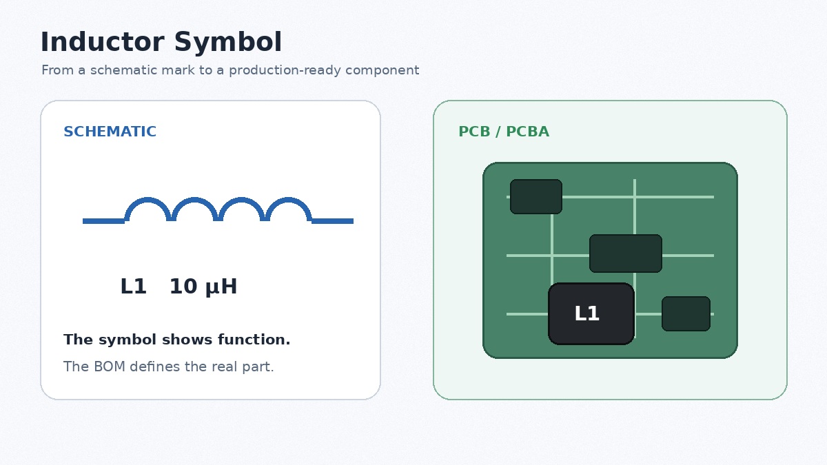
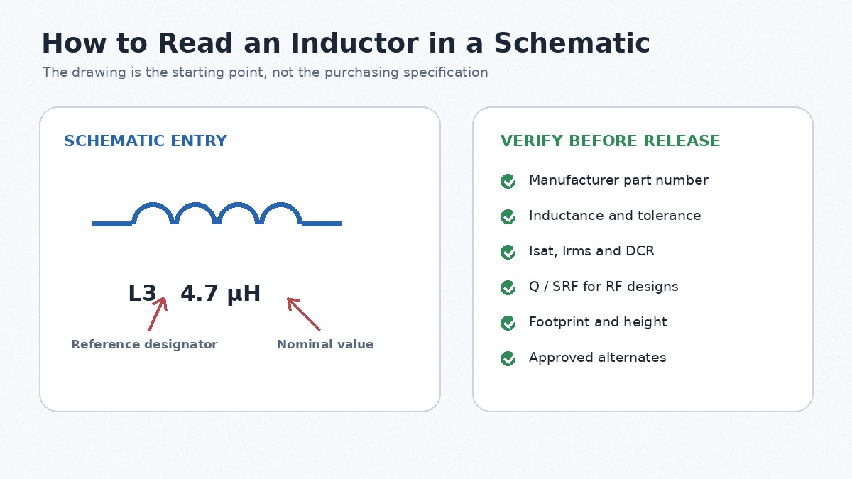
The basic electrical inductor symbol is a series of curved loops between two terminals. It represents a conductive winding, not the exact number of turns or the component’s physical shape. A schematic may draw the loops horizontally or vertically without changing the electrical meaning. The reference designator normally starts with L, such as L1 or L203, and the inductance value is stated in henries, usually microhenries (uH) or nanohenries (nH) on PCB designs.
The symbol belongs to the logical schematic. It does not define whether the real component is a molded SMD power inductor, a small RF chip inductor, a common through-hole choke or a toroid. That physical decision is carried by the manufacturer part number, schematic properties, BOM and PCB footprint. A correct design keeps those records linked so that L1 cannot be assigned a symbol for one function and a land pattern for an incompatible package.
Why Is Inductance Represented by L?
Electrical schematics conventionally use L as the quantity and reference letter for inductance. The SI unit is the henry, written H. A value marked 10 uH beside L1 therefore means that the component’s nominal inductance is 10 microhenries; it does not describe its current capacity or resistance.
The voltage-current relationship is v = L di/dt. A larger inductance produces a larger voltage for the same rate of current change. Stored magnetic energy is W = 1/2 L I². These relationships explain why inductors smooth current in converters and filters, and why an interrupted inductive current can generate a large voltage transient. Real components also contain winding resistance, parasitic capacitance and core loss, so the ideal formula must be combined with datasheet limits.
How Does an Inductor Work in a Circuit?
Current through the winding creates magnetic flux. When the current changes, the changing flux induces a voltage that opposes that change. Under steady DC conditions, an ideal inductor eventually behaves like a short circuit. A real inductor retains its DC resistance and may heat from copper and core losses. At increasing frequency, inductive reactance rises according to XL = 2 pi fL until parasitic capacitance becomes significant near the self-resonant frequency.
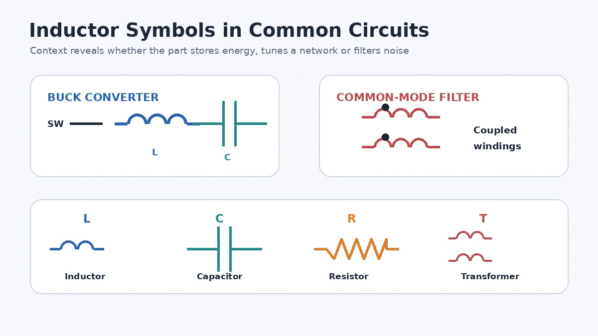
In a buck converter, the inductor receives pulsed energy from the switching node and delivers a smoother current to the output. In an LC filter, it impedes high-frequency current while the capacitor diverts unwanted energy. In an RF matching network, a few nanohenries can tune impedance, but the pad geometry and nearby copper can contribute enough parasitic inductance and capacitance to alter the intended value.
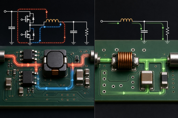
What Are the Main Inductor Symbols?
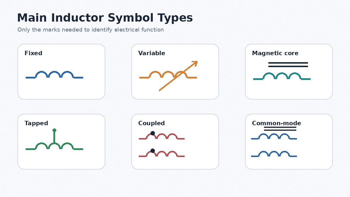
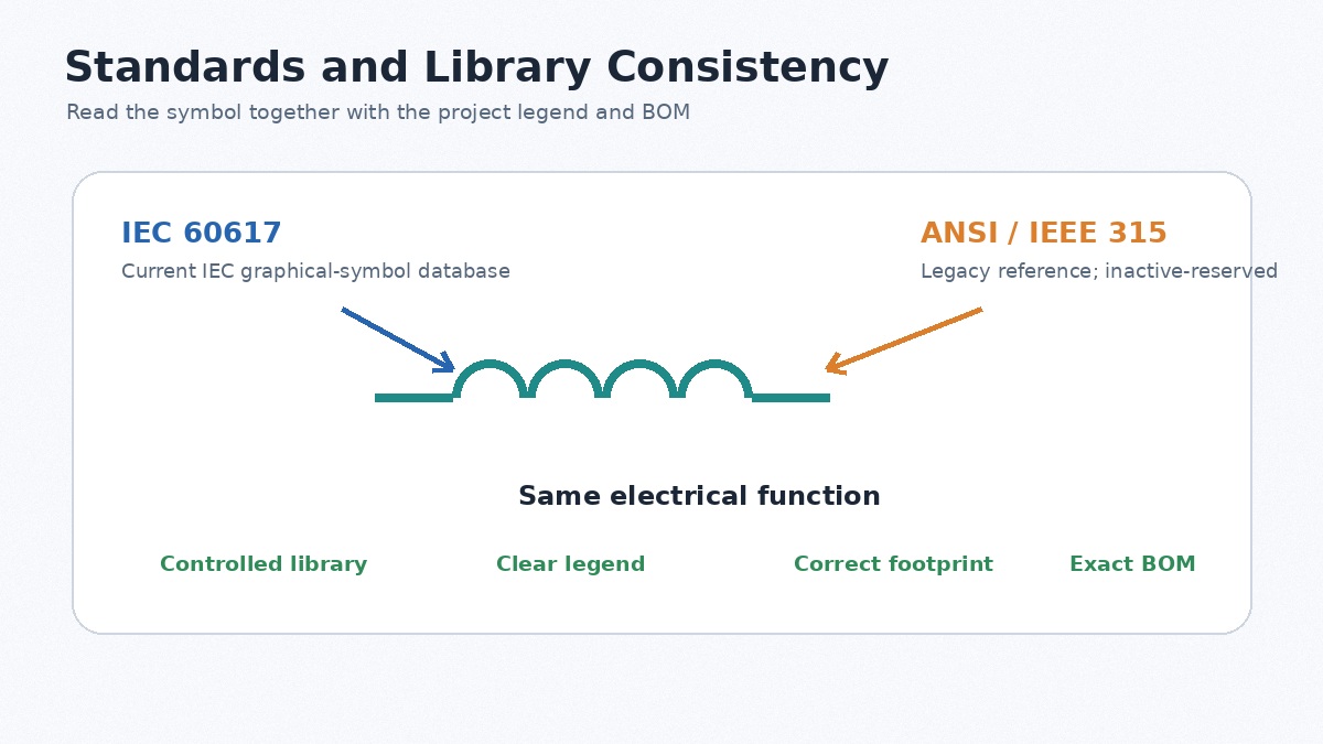
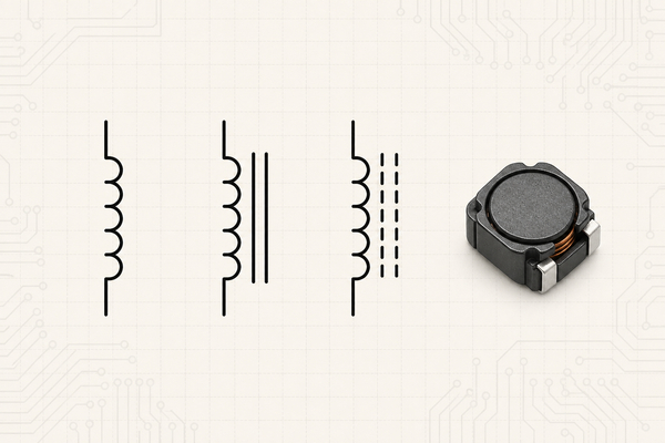
Most inductor symbols begin with the same coil form. Additional marks tell the reader what magnetic structure or electrical behavior matters in that circuit. The exact graphic style can vary between IEC, ANSI/IEEE and CAD libraries, so a project’s symbol legend and component properties remain authoritative.
| Symbol type | Typical graphic feature | What it communicates |
|---|---|---|
| Fixed or air-core inductor | Coil with no parallel core lines | Fixed inductance; air core may be inferred when no magnetic-core mark is used |
| Iron-core inductor | Coil beside two solid parallel lines | Ferromagnetic iron or laminated core |
| Ferrite-core inductor | Coil beside dashed parallel lines in many libraries | Ferrite magnetic core |
| Variable inductor | Diagonal arrow through or across the coil | Adjustable inductance |
| Tapped inductor | One winding with an intermediate terminal | Electrical connection to part of the winding |
| Coupled inductors | Two or more coils with core lines and often polarity dots | Magnetic coupling and winding polarity |
A schematic can also use specialized inductor symbols for saturable reactors, delay lines, current transformers or common-mode chokes. Do not select a component from the icon alone. Open its properties and check the description, part number, value, footprint and datasheet.
How Do Air-Core, Iron-Core and Ferrite-Core Symbols Differ?
An air-core symbol normally has no core lines. Air does not saturate like a ferromagnetic core and has low core loss, which can suit RF and high-frequency resonant circuits, but achieving high inductance generally requires more turns or a larger structure. The physical part may be an exposed helical coil even though the schematic only shows a generic winding.
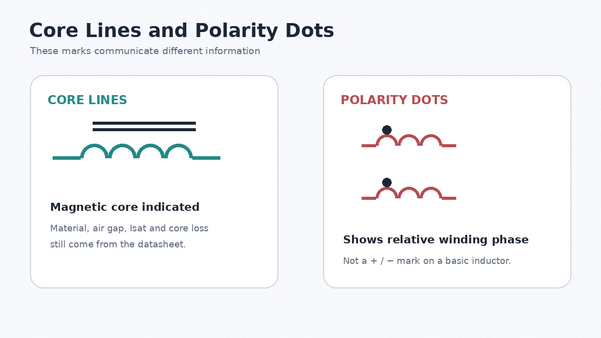
An iron core inductor symbol usually adds two solid lines beside the coil. Iron or laminated steel cores are associated with lower-frequency magnetic components and energy storage where size and loss targets permit. A ferrite symbol often uses interrupted or dashed core lines. Ferrite materials have high electrical resistivity and are widely used in switching power, EMI suppression and high-frequency magnetics. Symbol conventions can differ across libraries, so the component description must state the actual core material.
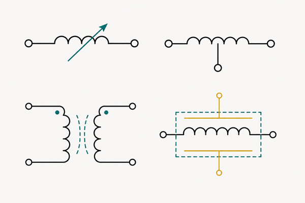
What Do Variable, Tapped, Coupled and Shielded Inductor Symbols Mean?
A diagonal arrow identifies a variable inductor. The adjustment may be mechanical, such as moving a core, and the datasheet defines its range and tuning method. A tapped symbol adds a terminal partway along one winding. The tap provides a selected turns ratio or impedance point, but it must not be mistaken for two independent windings.
Coupled inductor symbols show two or more windings sharing magnetic flux. Polarity dots identify corresponding instantaneous winding polarity; reversing one winding changes the phase relationship and can prevent a converter or filter from operating correctly. A common-mode choke is a coupled component whose windings carry opposing signal currents while presenting high impedance to common-mode noise.
Shielding may be communicated by a dedicated library symbol, an enclosure mark, a part description or simply the selected manufacturer part. It is not represented identically in every schematic standard. The BOM should explicitly identify shielded or unshielded construction when radiated field, magnetic coupling or mechanical robustness matters.
How Do IEC and ANSI/IEEE Inductor Symbols Differ?
IEC 60617 provides an international database of graphical symbols for electrotechnical diagrams. ANSI/IEEE practices and individual CAD libraries may render the winding with semicircular loops, a compact curved line or a rectangular form. Core, tap and adjustability marks can also differ in spacing and orientation. These drawing differences do not change the underlying circuit behavior.
A project should use one approved symbol library rather than mixing graphics copied from unrelated sources. Each symbol needs a unique library name, correct pin count, visible reference designator, value field and verified footprint association. If a supplier drawing uses another convention, compare terminal numbers and winding polarity rather than judging equivalence by appearance.
How Do You Read an Inductor Symbol in a Circuit?
Start with connectivity, then inspect properties. In an inductor symbol circuit example, L1 might connect a switching node to an output capacitor, while L2 may sit in series with an RF signal or power input. The surrounding topology identifies the likely function more reliably than the coil icon by itself.
- Trace both terminals and identify the source, load, return path and nearby switching devices or capacitors.
- Read the reference designator, nominal inductance and tolerance.
- Open the BOM entry to confirm the manufacturer part number and approved alternatives.
- Check Isat, Irms, DCR, SRF, Q, operating temperature and core-loss data that apply to the circuit.
- Verify the footprint, pin numbering, orientation and assembly notes against the datasheet.
For a switching regulator, also compare the selected part with the controller vendor’s ripple-current calculation and transient requirements. For an RF circuit, evaluate the component model at the actual frequency; nominal inductance measured at a low test frequency may not predict its behavior close to self-resonance.
How Can You Distinguish Inductor, Transformer, Resistor and Capacitor Symbols?
A single coil is normally an inductor. Two or more closely aligned coils with a core and polarity marks often represent a transformer or coupled inductor; the circuit function and part description resolve the distinction. A resistor uses a zigzag or IEC rectangular symbol, while a capacitor uses two plates, with one curved plate or a polarity mark for certain polarized types.
Appearance alone is insufficient for multi-winding magnetics. A flyback transformer can resemble coupled inductors, while a common-mode choke can resemble a transformer. Terminal count, dot convention, turns ratio, isolation requirement and BOM description establish the actual component. Library names should use functional terms such as “common-mode choke, two-line” rather than a vague label such as “coil.”
What Information Does the Schematic Symbol Not Show?
The schematic symbol communicates electrical intent, but it usually omits the limits that determine whether the real inductor survives and performs correctly.
- Inductance tolerance and bias behavior: inductance can decrease as DC current approaches saturation.
- Isat and Irms: saturation current and thermal current are different ratings and may use different temperature-rise criteria.
- DCR: winding resistance contributes conduction loss, voltage drop and temperature rise.
- SRF and Q: parasitic capacitance limits the frequency range in which the component remains inductive.
- Core loss: switching frequency, ripple waveform, flux swing and temperature affect magnetic loss.
- Package and shielding: dimensions, termination style, magnetic shielding, weight and vibration behavior affect PCB implementation.
These parameters should reside in the approved BOM and design calculations. A substitution based only on equal microhenry value can increase loss, saturate during peak current, shift an RF network or fail the available PCB footprint.
How Should an Inductor Footprint Be Designed on a PCB?
Use the component manufacturer’s recommended land pattern as the starting point. Confirm pad dimensions, solder mask opening, paste coverage, courtyard, component height and pin-one or polarity information where applicable. For a heavy component, include mechanical clearance and consider shock, vibration and board flex. Do not enlarge pads casually: excessive solder can promote floating or tilt, while undersized pads can reduce joint reliability.
On a switching regulator, place the power inductor close to the switch, diode or synchronous MOSFETs and output capacitors specified by the topology. Keep the high di/dt loop compact, use copper widths suitable for current and avoid routing sensitive feedback or analog traces beneath an unshielded magnetic component. A conventional FR4 PCB can support many power and filtering applications when copper thickness, thermal rise and stack-up are verified.
High-frequency matching networks need tighter parasitic control. On an RF PCB, pad length, ground-via placement, trace width and component orientation can alter the effective inductance and impedance. Use the vendor’s S-parameter or equivalent-circuit model when available and keep the measured reference plane consistent with the PCB model.
How Are Inductors Assembled and Inspected on PCBs?
Most chip and molded power inductors use SMT reflow. Through-hole coils and toroids may use wave soldering, selective soldering or manual processes approved for the assembly. The thermal profile must respect the component’s termination, body material and moisture limits. Large thermal mass can change local solder behavior, and heavy parts may need adhesive or mechanical support for vibration environments.
Inspection should match the termination geometry. 3D solder paste inspection can verify paste before placement, AOI can check presence, offset, polarity marks and visible joints, and X-ray can support packages with hidden or difficult-to-see terminations. Electrical or functional testing is still needed to detect an incorrect value, open winding, saturation-related behavior or circuit-level noise that visual inspection cannot establish.
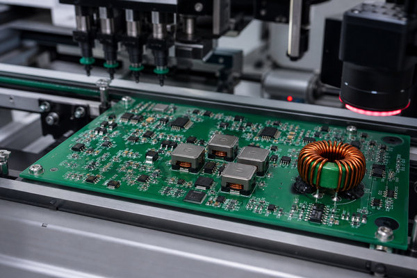
EBest Circuit (Best Technology) supports SMT, THT and mixed PCB assembly, with minimum SMD capability down to 01005 and inspection options including 3D SPI, AOI, X-ray and functional testing. Maximum capability depends on the package, board dimensions, design complexity, quantity and engineering review; the selected inductor remains a component specified by its manufacturer datasheet.
Where Are Inductors Used?
Power converters use inductors to store energy and control ripple current. Input and output filters use them with capacitors to attenuate conducted noise. RF circuits use chip inductors in impedance matching, bias networks, resonators and filters. Common-mode chokes suppress noise on power, USB, Ethernet and other differential interfaces. Audio crossovers, sensors, wireless charging systems and motor drives use magnetic components for filtering, energy transfer or current control.
The application determines which parameter dominates. A power inductor emphasizes saturation current, thermal current, DCR and core loss. An RF inductor emphasizes Q, SRF, tolerance and a frequency-dependent model. An EMI choke emphasizes common-mode impedance, leakage inductance, insulation and line current. The schematic coil may look similar in every case, but the parts are not interchangeable.
FAQ About Inductor Symbols
What is the unit shown with an inductor symbol?
The SI unit is the henry (H). PCB schematics commonly use microhenries (uH) and nanohenries (nH). Always distinguish the value from the reference designator, such as L1.
Does an air-core inductor need a different symbol?
A coil without core lines is commonly used for a fixed or air-core inductor. Because libraries vary, the component description and part number should explicitly identify air-core construction when it matters.
What does the arrow across an inductor mean?
The arrow marks a variable or adjustable inductor. Its adjustment range and mechanism come from the datasheet, not from the arrow geometry.
What do dots beside coupled inductor symbols mean?
The dots mark corresponding winding polarity. Currents entering dotted terminals produce magnetic flux with the same reference polarity. Correct dot orientation is essential in coupled converters and transformers.
Can one symbol represent any inductor package?
Yes, one logical symbol can be reused across many packages, but each component record must link to the correct footprint and BOM part. A generic symbol never authorizes a generic footprint.
Conclusion
The inductor symbol identifies magnetic energy storage, while core lines, arrows, taps and polarity dots communicate specific behavior. Reliable hardware requires one more layer of checking: link the symbol to the correct value, datasheet limits, BOM part and physical footprint, then review placement, soldering and inspection for the actual circuit. For PCB fabrication or assembly support, contact EBest Circuit (Best Technology) at sales@bestpcbs.com.