

PCB thermal hotspot map is a visual representation of temperature distribution across a PCB, used to identify high-temperature regions and optimize thermal performance. This article explains how hotspot maps are created, interpreted, and applied in real PCB design to improve reliability and efficiency.
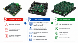
Many engineers face recurring thermal challenges. What are the most common pain points?
- Hotspots appear unexpectedly after assembly
- Components fail early due to overheating
- Thermal simulation results don’t match real testing
- Heat dissipation design increases cost without clear results
- PCB layout constraints limit thermal optimization
To address these issues effectively, a structured thermal strategy is required.
- Identify hotspots early using thermal analysis
- Optimize layout for heat distribution
- Use appropriate materials and stack-up
- Apply thermal vias and copper balancing
- Validate design with simulation and real testing
EBest Circuit (Best Technology) is a professional PCB and PCBA manufacturer with strong expertise in thermal-optimized PCB design and manufacturing, including high-power boards, metal core PCBs, and multilayer stack-ups. We provide one-stop services from PCB fabrication to PCBA, helping engineers reduce thermal risks and improve product reliability. Pls feel free to contact us via sales@bestpcbs.com.

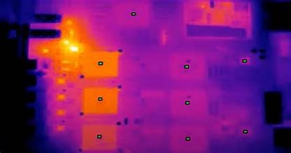
What Is a PCB Thermal Hotspot Map and Why Does It Matter in PCB Design?
A PCB thermal hotspot map is a temperature heatmap that shows where heat accumulates on a board.
Key Functions
- Identify overheating components
- Evaluate thermal distribution
- Guide layout optimization
- Improve reliability
Typical Hotspot Areas
- Power ICs
- MOSFETs
- High-current traces
- Dense BGA regions
A PCB thermal hotspot map is the foundation for thermal-aware PCB design.

What Causes Thermal Hotspots on a PCB?
Thermal hotspots occur when heat generation exceeds heat dissipation.
Main Causes
- High power density components
- Narrow or long high-current traces
- Poor copper distribution
- Inadequate airflow
- Improper component placement
Hotspots result from imbalance between heat generation and heat removal.
How Is a PCB Thermal Hotspot Map Created (Simulation vs. Measurement)?
Thermal hotspot maps are generated using simulation and real measurement.
Methods Comparison
| Method | Description | Use Case |
|---|---|---|
| Simulation | CFD or EDA tools | Design stage |
| Measurement | Infrared camera or sensors | Validation stage |
Key Steps
- Build thermal model
- Define boundary conditions
- Run simulation
- Validate with measurement
Simulation predicts, measurement confirms.
How to Read a PCB Thermal Hotspot Map Like an Engineer?
Understanding a thermal map requires interpreting temperature gradients.
Key Indicators
- Red or white indicates critical hotspots
- Yellow indicates moderate heat
- Blue indicates low temperature
What to Focus On
- Temperature peaks
- Heat flow direction
- Thermal clustering
Correct interpretation reveals thermal risks clearly.
What Is Thermal Resistance and How Does It Cause Hotspots?
Thermal resistance determines how easily heat flows.
Formula
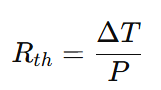
Key Insights
- Higher resistance means worse heat dissipation
- FR4 has relatively high thermal resistance
- Copper reduces thermal resistance significantly
Thermal resistance is the root cause of heat accumulation.
How Do PCB Materials and Stack-Up Affect Thermal Hotspots?
Material selection directly impacts thermal behavior.
Material Comparison
| Material | Thermal Conductivity | Application |
|---|---|---|
| FR4 | Low | Standard PCB |
| High Tg | Medium | High temperature boards |
| MCPCB | High | Power electronics |
| Ceramic | Very high | RF and aerospace |
Key Factors
- Copper thickness
- Layer structure
- Dielectric properties
Material choice defines thermal performance limits.
How Does Component Placement Affect PCB Thermal Hotspots?
Component placement determines heat distribution.
Design Guidelines
- Distribute high-power components evenly
- Keep sensitive parts away from heat sources
- Place heat sources near airflow paths
- Avoid clustering
Good placement reduces thermal concentration.
How to Reduce PCB Thermal Hotspots with Routing and Copper Design?
Routing affects both electrical and thermal performance.
Optimization Methods
- Use wider traces for high current
- Increase copper thickness
- Shorten trace length
- Use solid copper planes
Routing optimization reduces heat generation effectively.
How Do Thermal Vias and Heat Sinks Reduce Hotspots?
Thermal vias and heat sinks enhance heat transfer.
Key Techniques
- Thermal vias under power components
- Via-in-pad design
- Heat sink attachment
- Copper plane connection
These structures create efficient thermal pathways.
What Cooling Methods Help Control PCB Hotspots?
Cooling methods can be passive or active.
Cooling Types
- Passive cooling using copper planes and heat sinks
- Active cooling using fans
- Advanced cooling using heat pipes or TEC
Cooling ensures heat is removed from the system efficiently.
Common PCB Thermal Hotspot Design Mistakes and How to Avoid Them
Common Mistakes
- Ignoring thermal simulation
- Clustering high-power components
- Insufficient copper usage
- Poor via design
- Improper airflow planning
How to Avoid
- Perform early thermal analysis
- Optimize layout spacing
- Use proper materials
- Validate before production
Avoiding these mistakes improves reliability.
In Conclusion, PCB thermal hotspot map is a critical tool for identifying and controlling heat distribution in PCB design. By combining simulation, layout optimization, and proper material selection, engineers can significantly improve thermal performance and reliability.
EBest Circuit (Best Technology) provides advanced PCB and PCBA solutions for high thermal performance applications, helping customers achieve stable and reliable designs. Pls feel free to contact us via sales@bestpcbs.com.
FAQs About PCB Thermal Hotspot Map
What tools are used for PCB thermal hotspot analysis?
Common tools include ANSYS, FloTHERM, and Altium Designer.
How do you validate PCB thermal performance before production?
Use simulation, prototype testing, and infrared imaging.
What temperature is considered a hotspot in PCB design?
Typically above 85 to 100 degrees Celsius depending on components.
How many thermal vias are enough under a power IC?
As many as possible within design and manufacturing limits.
Can FR4 handle high thermal hotspots?
FR4 can handle moderate heat, but high-power designs require advanced materials.
You may also like


Tags: PCB Thermal Hotspot Map