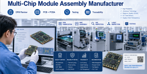
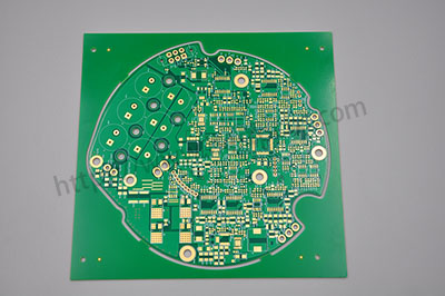
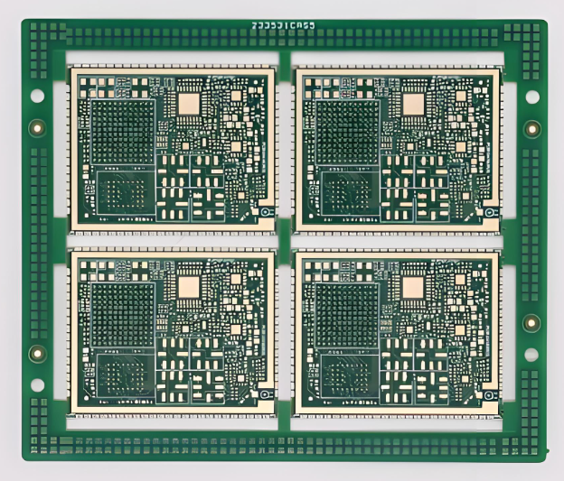
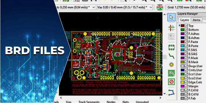
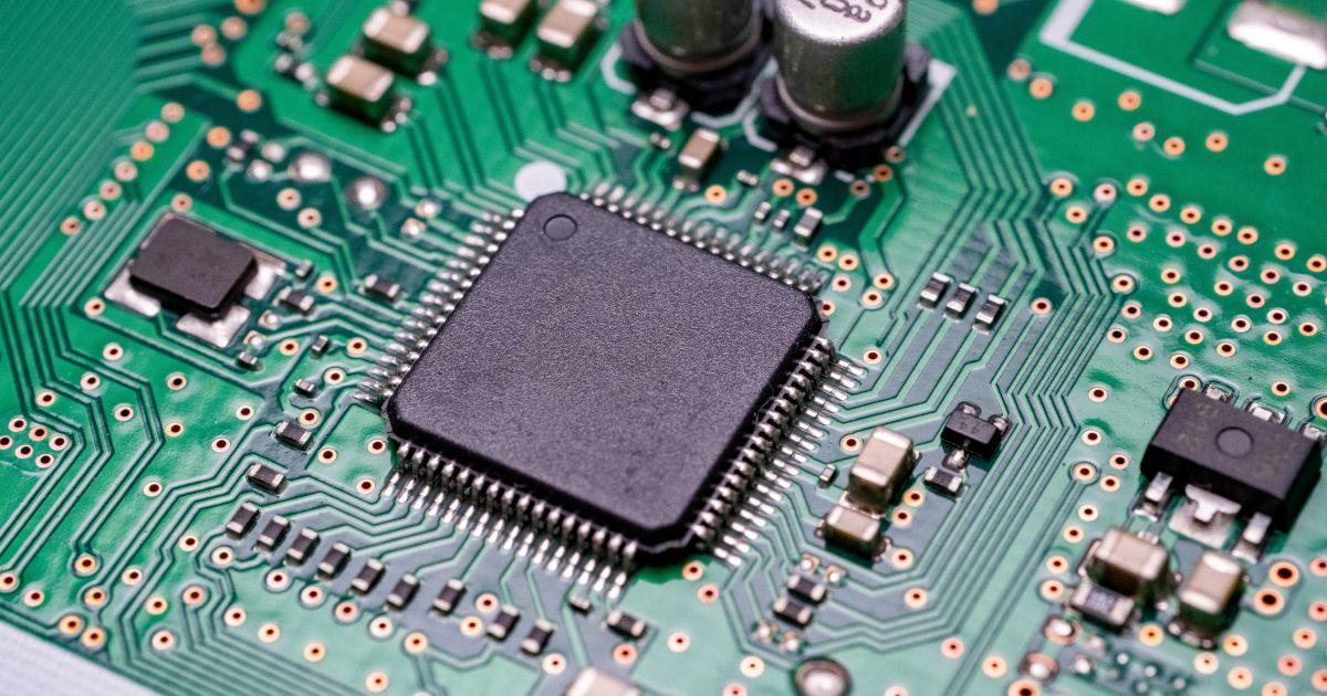
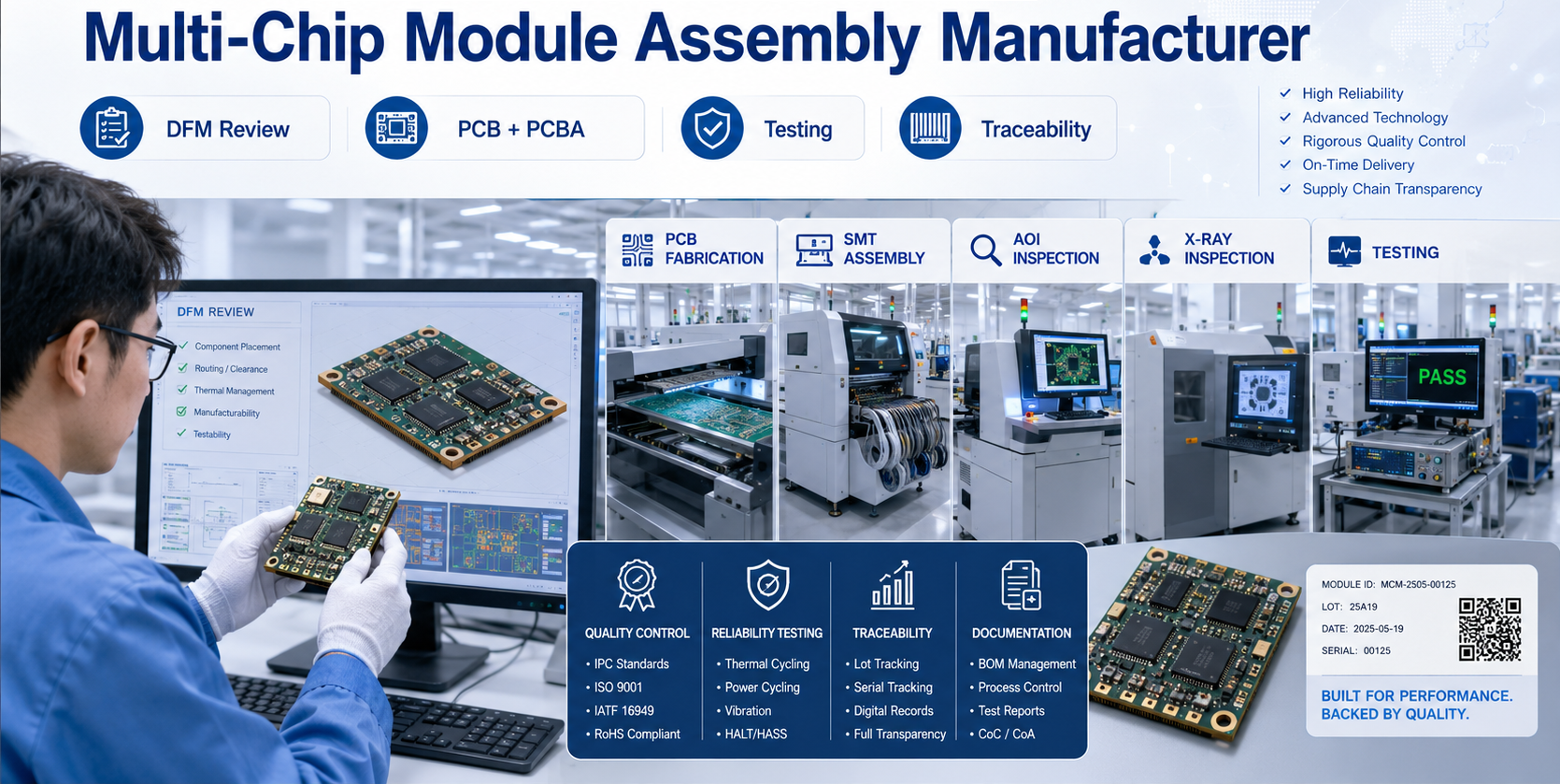
A multi chip module places two or more semiconductor dies on a shared substrate so that the completed package can operate as one component. The approach can shorten critical connections, combine dies made with different processes and reduce the area required on the system board. Those benefits are not automatic: substrate technology, die attachment, power delivery, heat flow, test coverage and the PCB interface must be designed as one system.
What Is a Multi Chip Module?
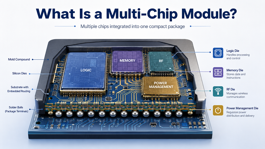
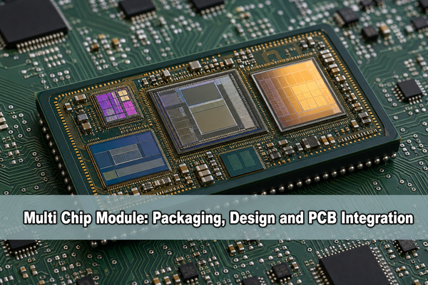
A multi chip module, or MCM, is an electronic package or module containing multiple interconnected semiconductor dies. Logic, memory, analog, RF, sensor or power functions can share one package substrate. The module presents an external interface such as BGA balls, LGA lands or leads, allowing the system to handle it as a single component.
The defining point is the packaging hierarchy. Bare dies and their internal connections belong to the MCM. The larger board that receives the completed module is the system PCB. A board carrying several conventionally packaged ICs is a PCB assembly, but it is not automatically an MCM. Modern terminology overlaps with system-in-package and chiplet packaging, so the physical implementation and functional partition matter more than the label alone.
How Does a Multi Chip Module Work?
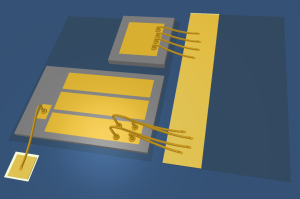
Each die performs a defined function and communicates through conductors in or on the shared substrate. Wire bonds can connect die pads to substrate pads. Flip-chip bumps can connect a die face-down to fine-pitch routing. An interposer or redistribution layer can provide much denser die-to-die paths than a conventional system PCB.
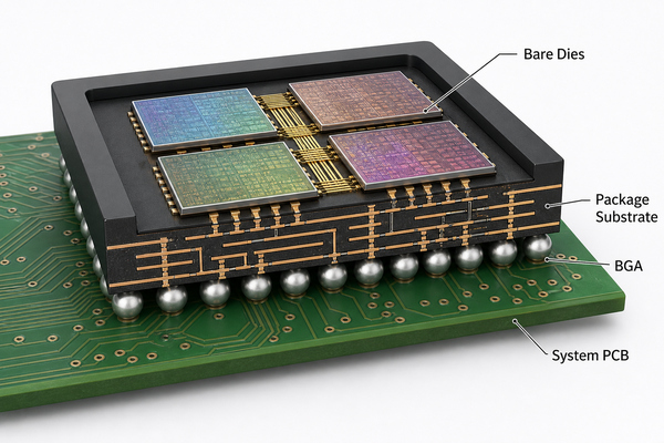
The substrate redistributes thousands of fine die connections to an external pitch that assembly equipment and the system PCB can support. It also carries power and ground, supports decoupling, controls impedance and provides part of the thermal path. Encapsulation, a lid, underfill or a heat spreader may protect the dies and stabilize the structure. The finished module is then soldered or mechanically connected to the system board.
What Are the Main Multi Chip Module Packaging Types?
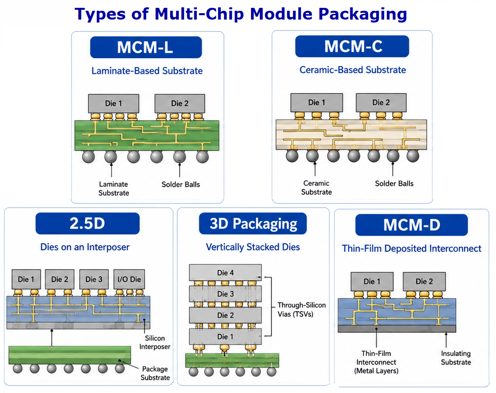
Traditional multi chip module packaging is classified by how the interconnect substrate is made. MCM-L uses laminate technology, MCM-C uses ceramic processing and MCM-D uses deposited thin-film conductors and dielectrics. Modern packages may add silicon or organic interposers, redistribution layers, embedded bridges, fan-out structures or vertical stacking.
The class name does not fully define performance. A fine-line build-up laminate can outperform an older laminate construction, while a ceramic substrate may be chosen for dimensional or thermal reasons rather than maximum routing density. Die I/O pitch, signal speed, power density, module size, production volume and test strategy must be evaluated together.
How Do MCM-L, MCM-C and MCM-D Compare?
The practical decision starts with routing density, thermal expansion, heat flow and process maturity. The table summarizes the main differences without treating one technology as universally superior.
| Type | Substrate and process | Typical strengths | Primary constraints |
|---|---|---|---|
| MCM-L | Organic laminate fabricated with advanced PCB or build-up processes | Established supply chain, larger formats, practical multilayer routing and cost scaling | CTE, moisture behavior, warpage and fine-feature limits depend on material and buildup |
| MCM-C | Multilayer ceramic, commonly co-fired or thick-film processed | Dimensional stability, electrical insulation, temperature capability and controlled material properties | Higher material/process cost, brittle handling and shrinkage control |
| MCM-D | Deposited thin-film metal and dielectric layers on a rigid base | Fine routing, small vias and short high-performance interconnects | Process complexity, equipment cost, layer buildup time and yield sensitivity |
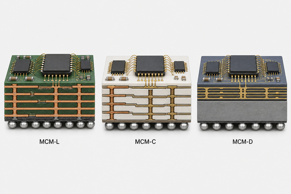
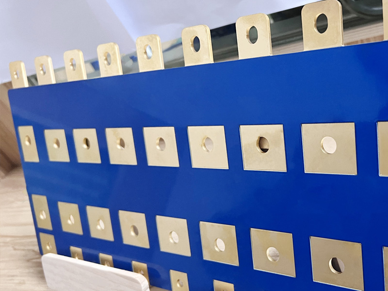
An MCM-L may use a multilayer FR4 PCB-like process when its electrical and thermal limits are appropriate. MCM-C can use a ceramic PCB or ceramic circuit substrate when insulation, dimensional stability or heat transfer justifies it. MCM-D is closer to thin-film microfabrication than ordinary PCB manufacturing.
What Is a Wafer Level Multi Chip Module?
A wafer level multi chip module uses wafer-level redistribution, fan-out or stacking processes to integrate multiple dies before the final package is completed. In a fan-out flow, known-good dies can be placed in a reconstituted wafer or panel, embedded in molding compound and connected with redistribution layers. Wafer-level system-in-package processes can place dies, passives or sensors side by side and can also support stacked configurations.
WMCM is not one fixed construction. The term may describe different multi-die wafer-level implementations, so package drawings must define die placement, redistribution layers, vertical connections, external ball pattern and thermal structure. It should not be used as a synonym for every MCM. The important distinction is that wafer-level processes form much of the package interconnect before singulation, unlike a laminate module assembled as an individual substrate.
What Matters in Multi Chip Module Design?
Multi chip module design is a chip-package-board co-design problem. Optimizing only die placement can leave an unrouteable substrate, an unstable power network or a poor thermal path. Start with the complete connectivity, power map, heat sources, package outline, external I/O and assembly constraints.
- Die placement: keep high-bandwidth die pairs close, but reserve room for escape routing, decoupling, keepouts, underfill flow and heat spreading.
- Signal integrity: control impedance, return paths, crosstalk, discontinuities and skew across die bumps, substrate routing, package balls and PCB traces.
- Power integrity: size power/ground planes, place decoupling by frequency and current demand, and model simultaneous switching noise and voltage drop.
- Thermal design: calculate die-level power maps rather than using only package-average power. Local hotspots can dominate junction temperature.
- Mechanical design: review die size, substrate thickness, CTE mismatch, lid stiffness, underfill, molding and board attachment for warpage and fatigue.
- Test access: plan die screening, boundary scan, package test, thermal monitoring and system diagnostics before routing is fixed.
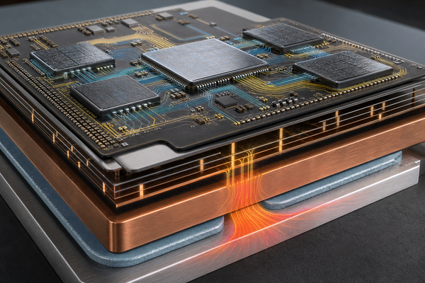
Short internal connections can reduce parasitic resistance, inductance and capacitance, but density also makes coupling and current concentration harder to control. Package and PCB models should therefore be analyzed together for fast interfaces. The same return-path discipline described in high-speed digital PCB design remains relevant after the signals leave the package.
How Is a Multi Chip Module Connected to a PCB?
The finished MCM commonly uses a BGA or LGA interface. Its ball or land map fans out into the system PCB through dog-bone vias, via-in-pad structures or microvias. The correct escape pattern depends on pitch, ball diameter, pad design, layer count, signal class, power distribution and assembly process. High-I/O modules can require an HDI PCB with laser-drilled microvias and sequential buildup.
The PCB stack-up must preserve return paths under high-speed signals, provide low-impedance power delivery and conduct heat away from the package. Thermal vias, internal copper planes, local copper density and a chassis or heatsink interface may all contribute. The board should also account for package warpage, component keepouts, rework clearance and the soldering profile.
Assembly data must identify package outline, pin-one orientation, paste stencil design, moisture sensitivity, reflow limits and inspection requirements. Very dense BGA interfaces usually need X-ray because optical inspection cannot see the internal solder joints.
How Do MCM, Chiplet, SiP and Monolithic IC Differ?
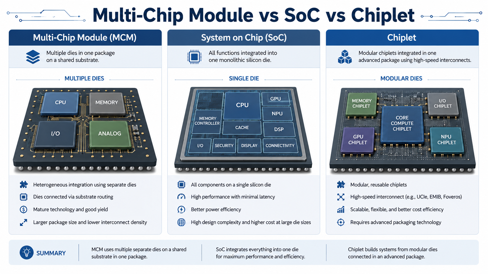
These terms describe different levels of integration. A chiplet is a die intended to be combined with other dies. An MCM is the package or module that interconnects multiple dies. A system-in-package usually emphasizes a complete system function and may include dies, passives, sensors, filters or MEMS. A monolithic IC integrates its functions on one die.
| Term | Physical meaning | Design implication |
|---|---|---|
| Monolithic IC | Functions fabricated on one semiconductor die | Very short on-die links, but die size, process compatibility and yield constrain integration |
| Chiplet | A modular die designed for multi-die integration | Requires a defined die-to-die interface and compatible package architecture |
| MCM | Multiple dies interconnected on a shared substrate or interposer | Package-level electrical, thermal, mechanical and test co-design is essential |
| SiP | Multiple functional elements combined as a packaged system | May include MCM structures plus passives, sensors, RF filters or other components |
The phrases multi chip module vs MCM do not describe competing technologies; MCM is simply the abbreviation. Multi chip module vs chiplet is different: the chiplet is one building block, while the MCM is an integration vehicle that may contain several chiplets or conventional dies.
Why Do MCM GPUs Support Continued Performance Scalability?
GPU and accelerator designs use multiple compute dies or chiplets to increase compute resources without making one monolithic die continually larger. Specialized dies for compute, cache, memory interfaces and I/O can be manufactured with process technologies suited to each function, then connected in an advanced package. This can improve design reuse and can reduce the yield penalty associated with a very large die.
Scalability still depends on the interconnect. Bandwidth, latency, synchronization, cache coherence, memory placement, package power and cooling determine whether additional dies deliver useful performance. AMD, for example, describes current accelerator architectures that connect GPU chiplets, high-bandwidth memory, cache and I/O through on-package Infinity Fabric links. The package does not remove the need for efficient workload partitioning or software support.
MCM GPU designs create a system tradeoff rather than a guarantee that adding dies will scale performance linearly. More dies can increase communication traffic and hotspot interaction, so architecture, packaging and cooling must advance together.
Where Are Multi Chip Modules Used?
Multi chip modules are used when several functions need a compact, high-bandwidth or application-specific connection. The implementation varies widely by industry.
- High-performance computing: processors, GPUs, accelerators, cache and high-bandwidth memory packages.
- RF and wireless: power amplifiers, switches, filters, control ICs and passive networks in compact front-end modules.
- Automotive and industrial electronics: sensing, control, radar, power management and computing modules that require defined thermal and mechanical performance.
- Medical and sensor systems: mixed-signal processing, sensing and communications integrated within a small package.
- Aerospace and defense: dense computing or RF functions where size, weight, interconnect length and environmental qualification matter.
An intelligent power module may also integrate control and power semiconductor functions, but IPM and MCM are not interchangeable labels. The package construction, insulation structure, current path and thermal interface must be examined rather than inferred from the name.
What Can Go Wrong in Multi Chip Module Packaging?
Adding dies and interfaces creates more points that must be controlled. A design can be electrically correct and still fail because heat, stress, materials or test coverage were incomplete.
- Known-good-die risk: one defective die can reduce the yield and value of an otherwise completed module.
- CTE mismatch: silicon, organic laminate, ceramic, copper, molding compound and the system PCB expand differently during processing and operation.
- Warpage: uneven materials, copper distribution or cure shrinkage can distort the substrate and disturb bump or BGA coplanarity.
- Interconnect defects: non-wet joints, voids, opens, shorts, bond lift, bump fatigue and underfill voids may be hidden from optical inspection.
- Electrical coupling: dense signal, power and ground structures can create crosstalk, return-path breaks, resonances and simultaneous switching noise.
- Thermal interaction: one die can heat neighboring dies, while a package-average temperature hides a local hotspot.
Reliability is therefore conditional. Shorter connections can reduce some parasitics and board-level joints, but an MCM does not automatically outlast a single-die package. Material characterization, simulation, controlled assembly and qualification determine the result.
How Are Multi Chip Modules Inspected and Tested?
Inspection should follow the structure from die to system board. Wafer probing and known-good-die screening reduce the chance of packaging defective silicon. During module assembly, optical inspection can verify placement and wire bonds, while X-ray can reveal hidden bumps, BGA joints, bridges, opens and void patterns. Scanning acoustic microscopy may be used to detect delamination or underfill defects.
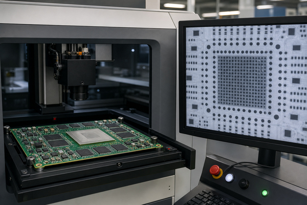
Electrical tests include continuity, shorts, parametric checks and functional operation. Boundary scan can improve access when physical probing is limited. Thermal cycling, temperature-humidity, high-temperature operating tests, mechanical stress and power cycling are selected according to the application and dominant failure mechanisms. At the system-board level, PCB assembly controls such as solder paste inspection, AOI, X-ray and functional testing verify the module-to-board interface. The existing guide to X-ray inspection in PCB assembly explains the value of hidden-joint imaging in more detail.
What Should Multi Chip Module Manufacturers Coordinate with PCB and PCBA Teams?
Multi chip module manufacturers and system-board teams must exchange interface data early. The package outline, ball map, pin functions, pitch, pad recommendation, allowed via structures, power map, thermal resistance model, warpage limit, moisture classification and reflow window affect PCB layout and assembly. Signal models and power-delivery models are needed when the module carries fast interfaces or high transient current.
The PCB team should return the proposed stack-up, fan-out geometry, impedance targets, plane assignment, thermal-via design and mechanical constraints. The assembly team should confirm stencil strategy, paste type, placement support, reflow profile, X-ray criteria, cleaning limits and rework access. Revision control is critical: a changed ball assignment or package drawing can invalidate both layout and test fixtures.
EBest Circuit (Best Technology) supports the PCB and PCBA side of this integration. Published capabilities include HDI line/space down to 2/2 mil, HDI holes down to 0.10 mm and BGA pitch down to 0.25 mm. Maximum capability depends on material, layer stack-up, board dimensions, design complexity, production quantity and engineering review. These capabilities do not mean EBest Circuit fabricates semiconductor dies or wafer-level MCM packages; the scope is the supporting PCB, ceramic circuit and board-level assembly work.
FAQ About Multi Chip Modules
Is a multi chip module the same as a chiplet?
No. A chiplet is a modular die. A multi chip module is the package or assembly that interconnects multiple dies; it may contain chiplets, conventional dies or both.
Is MCM the same as multi chip module?
Yes. MCM is the standard abbreviation for multi chip module. The exact physical construction still needs to be defined because MCM-L, MCM-C, MCM-D and wafer-level designs use different processes.
Can a multi chip module use both wire bonding and flip chip?
Yes. A heterogeneous module can use different attachment methods for different dies when the substrate layout, assembly sequence, wire clearance, underfill and thermal process are compatible.
What does “MCM GPU multi chip module GPUs for continued performance scalability” mean?
It refers to partitioning a GPU or accelerator across multiple compute, cache, memory or I/O dies and connecting them in one advanced package. Continued performance scaling depends on die-to-die bandwidth, latency, power, cooling and software efficiency, not only the number of dies.
Is wafer level multi chip module packaging the same as MCM-L?
No. MCM-L is based on a laminate substrate. Wafer-level multi-die packaging typically uses redistribution, fan-out, molding or stacking processes formed at wafer or panel scale before final singulation.
Can a finished MCM be assembled on a standard PCB?
Sometimes. The external pitch, I/O count, power, thermal load and signal speed determine whether a conventional multilayer board is sufficient or an HDI, high-frequency or ceramic solution is required.
Conclusion
A multi chip module can combine specialized dies, shorten internal connections and reduce system-board area, but its value depends on coordinated package, thermal, test and PCB design. MCM-L, MCM-C, MCM-D and wafer-level approaches solve different density, material and manufacturing problems. When a completed module needs an HDI, FR4 or ceramic system board and controlled PCBA integration, EBest Circuit (Best Technology) can review the PCB-side construction and assembly requirements. Contact sales@bestpcbs.com.