PCB manufacturing PCB manufacturing
Home > Blog

How Do You Choose a PCB Assembly Manufacturer in California?

August 26th, 2026

Before choosing a PCB assembly manufacturer in California, verify the actual build site, required assembly processes, material responsibility, inspection coverage, price basis and delivery assumptions. A nearby address is useful only when the quoted facility can build, inspect and document the specific product.

Hardware engineers need package and process compatibility; quality teams need acceptance evidence and traceability; buyers need comparable material, tooling, test, freight and schedule assumptions. All three teams should approve the same site identity, production route and acceptance plan before comparing quotations.

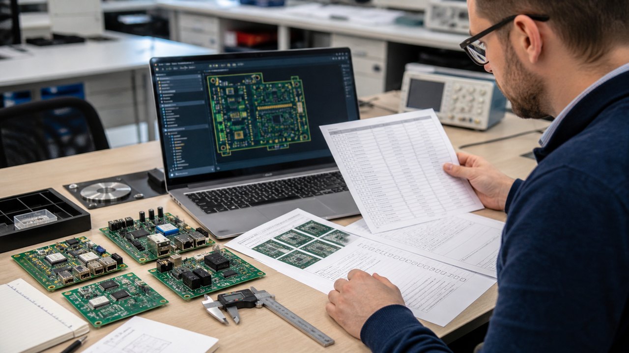
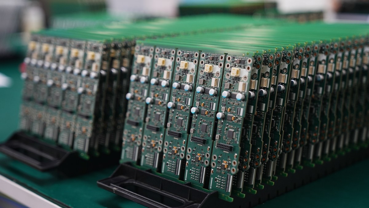
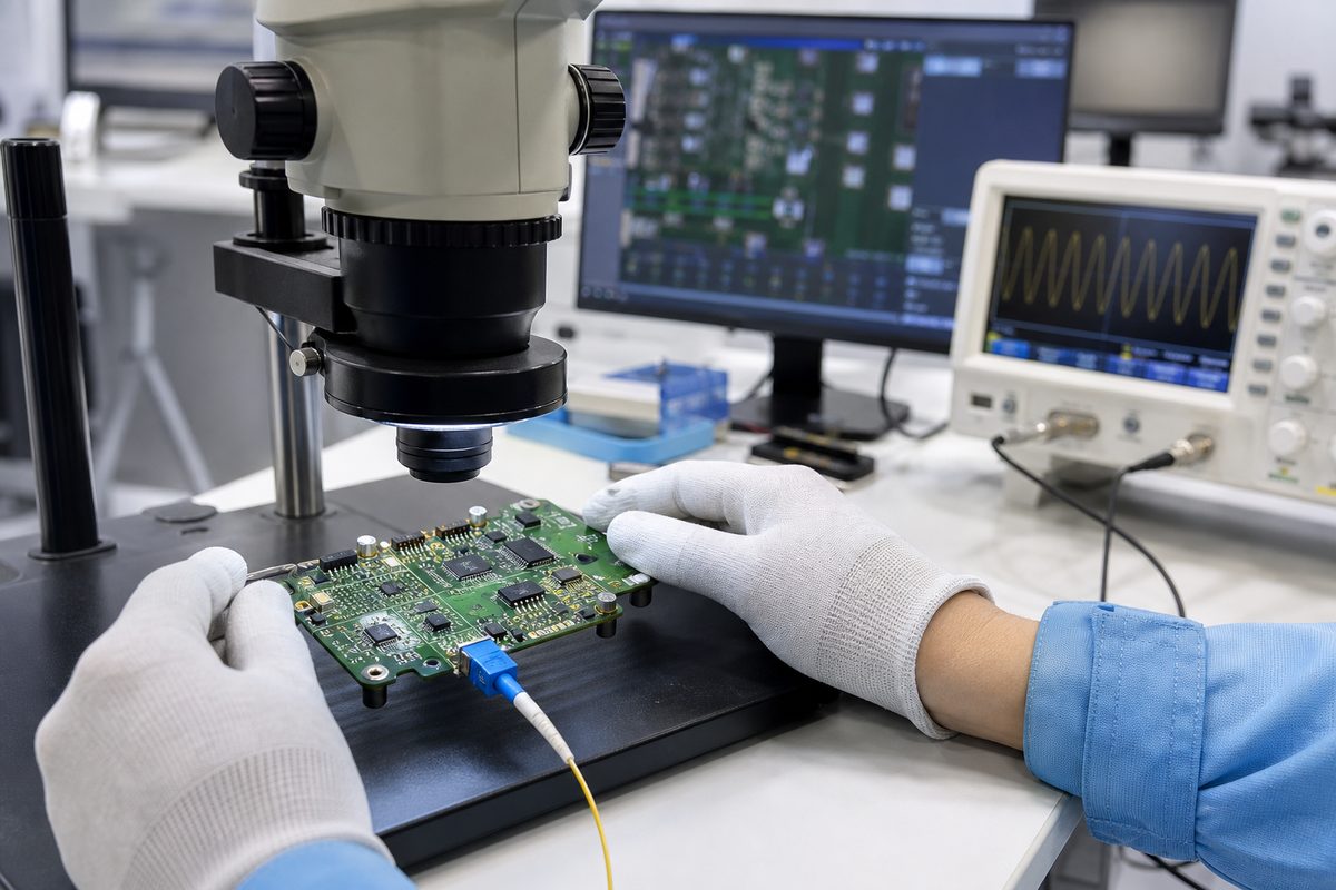
PCB Assembly Manufacturer in California, engineers reviewing an assembled PCB beside an SMT production line

What Should a PCB Assembly Manufacturer in California Provide?

The contracted service must match the order from material receipt through final acceptance. Buyers should identify which operations occur at the quoted California site, which are subcontracted and which remain the buyer’s responsibility.

  • Assembly scope: define SMT placement, through-hole assembly, mixed-technology processing, hand operations and any required depaneling or mechanical work.
  • Material scope: assign bare-board and component purchasing, approved-source control, substitution approval, incoming inspection and unused-material disposition.
  • Engineering scope: require DFM findings, BOM and footprint checks, stencil review, panel review and documented disposition of unresolved issues.
  • Verification scope: specify workmanship criteria, AOI or X-ray coverage, programming, electrical or functional testing and the records returned with the shipment.
  • Special-process scope: identify cleaning, conformal coating, cable installation, enclosure integration or other services only when the project needs them and the supplier confirms the responsible site.

The quotation and purchase order should name every included operation and handoff. If a process is outsourced, record the subcontracted scope, approval responsibility and acceptance evidence instead of treating the supplier’s general service list as the order plan.

How Can You Verify a PCB Assembly Manufacturer in California?

Verify the manufacturing location named for the order, not the headquarters or sales address. The quote should identify where placement, soldering, inspection and testing will occur and whether any material or data leaves that facility.

  • Legal and operating identity: match the company name and manufacturing address across the quotation, purchase order, certificate of conformance and invoice.
  • Site-specific capability: request confirmation that the named facility has the production line, inspection equipment, test resources and trained personnel required by the released product.
  • Order routing: state whether California assembly is mandatory, preferred or one option in a comparative quote, then require written approval before routing changes.
  • Subcontractor disclosure: identify outside PCB fabrication, coating, cable, environmental testing or other processes that affect product acceptance.
  • Certificate boundary: check the legal entity, site, service scope and current validity of any certificate used during supplier approval.

For export-controlled or customer-restricted work, establish the permitted data path, personnel access and manufacturing location before releasing controlled files. A California keyword or mailing address does not establish compliance.

Which Process Capabilities Should a PCB Assembly Manufacturer in California Offer?

A capable supplier must cover the processes the released assembly actually requires and show how each process is controlled. Buyers should compare the product’s packages, board construction, thermal mass, side count and test access with the supplier’s documented process route.
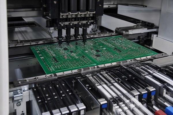
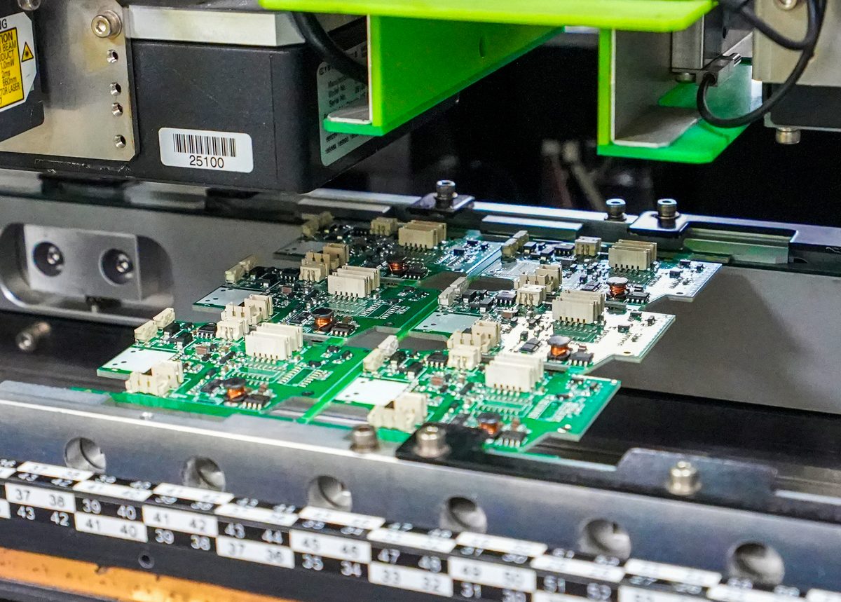
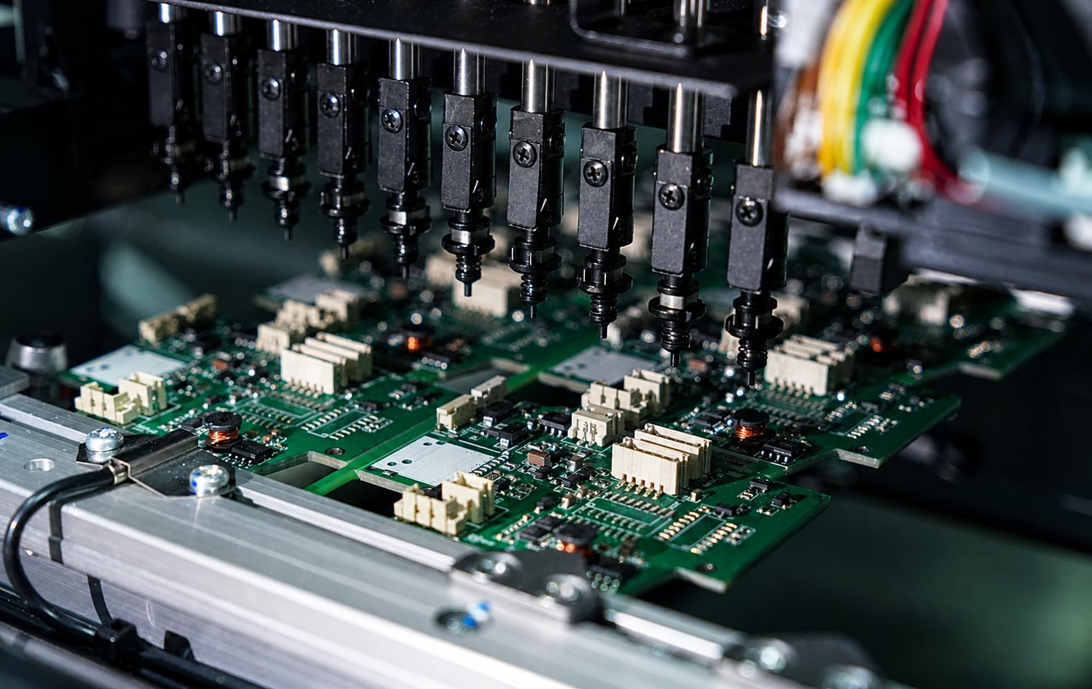
PCB Assembly Manufacturer in California, SMT placement equipment assembling a populated PCB panel
Process Capability to Verify Project Match Acceptance Evidence
Incoming control Board and component identity, quantity, packaging, moisture status and damage checks Approved manufacturers, date or lot restrictions, customer-owned material and storage limits Receiving record, discrepancy log and approved disposition
Stencil printing Stencil selection, aperture review, paste control and print inspection for the actual land pattern Fine-pitch leads, exposed pads, mixed thermal mass and double-sided assembly Stencil release, paste record and first-article inspection result
SMT placement Package handling, placement accuracy, feeder support, board support and program verification Smallest package, tallest component, board size, panel format and component-side count Approved machine program, first-article report and placement inspection
Reflow soldering Profile development, oven capacity, alloy control and thermal monitoring Component temperature limits, board thermal mass and mixed component population Approved profile, lot record and workmanship result
Through-hole soldering Wave, selective or controlled hand-soldering route with suitable fixtures and heat control Connector mass, hole fill requirement, component clearance and heat-sensitive parts Work instruction, process record and inspected solder-joint result
Hidden-joint inspection X-ray method and coverage appropriate to BGA, QFN or other bottom-terminated components Joint geometry, voiding risk, sampling plan and customer acceptance requirement Inspection images or report with disposition of suspect joints
Programming and test Firmware control, fixture interface, electrical limits, functional sequence and result capture Programming method, test access, required firmware revision and product-level pass criteria Controlled procedure, serial or lot-linked result and failure record
Optional finishing Cleaning, coating, labeling or mechanical integration performed under an approved route Residue limit, coating keep-outs, cure requirements, label data and enclosure interfaces Process traveler, inspection record and customer-approved completion criteria

A supplier does not need every optional process for every order. It does need a documented route for each required operation, a clear acceptance method and written approval before changing the route or subcontracting a controlled step.

How Do Turnkey and Consigned PCB Assembly Compare?

Turnkey assembly transfers purchasing responsibility to the supplier, while consigned assembly keeps material ownership and supply control with the buyer. The better model depends on component availability, approved-source restrictions, internal purchasing resources, inventory ownership and schedule risk.

Decision Area Turnkey Assembly Consigned Assembly Buyer Check
Material ownership Supplier purchases agreed bare boards and components Buyer supplies boards, components or complete kits When ownership and liability transfer
Approved sources Supplier buys from the approved manufacturer and channel list Buyer controls purchasing source before consignment AVL, traceability and substitution authority
Shortage management Supplier reports availability and proposes approved recovery actions Buyer replaces missing or unusable kit items Who owns line-stop risk and expedite cost
Incoming inspection Supplier verifies purchased material under the agreed plan Assembler checks consigned material against agreed receipt criteria Damage, moisture status, quantity and identity records
Excess and attrition Terms define attrition allowance and disposition of supplier-purchased excess Buyer normally supplies agreed overage and owns unused material Return, storage, scrap and replenishment terms
Cost visibility Quote combines material, purchasing service and assembly Assembly quote excludes the buyer’s material acquisition cost Compare total material, logistics and carrying cost
Schedule exposure Start date depends on supplier procurement and material receipt Start date depends on kit completeness and usable packaging Material-ready date and policy for incomplete kits
Best fit Teams seeking one commercial owner for sourcing and assembly Controlled, proprietary, allocated or buyer-owned components Internal purchasing capacity and risk ownership

Partial turnkey is useful when the buyer consigns proprietary or allocated items and the supplier buys the remaining BOM. Whatever the model, the purchase order should define substitutions, attrition, moisture-sensitive handling, excess inventory, unusable material and shortage escalation.

What Should Buyers Include in a PCB Assembly RFQ?

An RFQ should give the assembler one consistent production identity and enough information to price material, engineering, assembly, inspection, test and delivery. Conflicting revisions or an undefined test scope make price and lead-time comparisons unreliable.

  • Fabrication package: provide Gerber or approved intelligent data, drill files, outline, stackup, finish, controlled notes and the released board revision.
  • BOM: include manufacturer names, complete part numbers, quantities, reference designators, approved alternates and do-not-fit status.
  • Placement data: identify X/Y location, rotation, board side, origin convention and the same reference designators used by the BOM and drawing.
  • Assembly drawing: define polarity, hardware, special soldering, keep-outs, labels, workmanship criteria and any customer-controlled process note.
  • Test package: state the procedure, firmware, interfaces, fixtures, limits, expected output and who supplies each test resource.
  • Demand profile: separate prototype, pilot and recurring quantities, requested delivery dates, forecast assumptions and the delivery location.
  • Commercial boundary: assign purchasing responsibility, approved sources, substitutions, attrition, excess inventory, packaging, freight and tax treatment.

Ask the supplier to return an exceptions list with the quotation. Every exception should identify the affected file or line item, its cost or schedule effect and the decision required before material commitment.

How Should DFM and Component Sourcing Be Evaluated?

Evaluate DFM and sourcing by the decisions they produce, not by whether the supplier says a review was completed. Each finding should name the location or part, explain the manufacturing or supply consequence and record the approved response.

  • Footprint alignment: compare package dimensions, polarity, pin count and reference designators across the library, BOM, placement file and assembly drawing.
  • Solder-volume control: review fine-pitch apertures, exposed pads, mixed thermal mass and package combinations that may require a different stencil or paste strategy.
  • Panel handling: confirm rails, fiducials, tooling holes, component-to-edge clearance, board support and the intended depaneling method.
  • Supply status: check lifecycle, authorized availability, MOQ, moisture sensitivity, packaging condition and date or lot restrictions before purchase release.
  • Substitution authority: require written approval before changing manufacturer, part number, package, electrical rating or compliance attribute.

A useful DFM output shows marked locations, severity, the recommended correction, the party responsible for disposition and the revision that incorporates the final decision.

What Quality and Test Evidence Should Buyers Request?

Request evidence that matches the assembly’s actual failure risks and acceptance requirements. The order should state what is inspected or measured, the coverage, the applicable criteria, the disposition process and the record returned for each lot.

PCB Assembly Manufacturer in California, quality engineer inspecting populated circuit boards at a workbench
  • Solder-process record: identify the agreed workmanship requirement, alloy, controlled profile or soldering route and lot-linked process evidence.
  • First-article result: confirm component identity, polarity, orientation, placement and special assembly features before releasing the remaining lot.
  • AOI coverage: define the visible component and solder conditions inspected, plus the review and disposition of detected defects.
  • X-ray coverage: use it where hidden joints create a relevant risk, and state the components, sampling level and acceptance basis instead of requesting it by default.
  • Electrical or functional test: provide the procedure, fixtures, firmware, test limits and required result format; workmanship inspection cannot substitute for product-level function.
  • Traceability record: agree which board, component, process, inspection, test and shipment identities must be linked to the delivered assembly.

AOI, X-ray and functional testing answer different questions. The verification plan should combine only the methods needed to detect the product’s identified assembly and operating risks.

What Determines PCB Assembly Price and Lead Time?

Price and lead time are driven by material readiness, engineering setup, process complexity, verification scope, lot size and delivery terms. Geography matters, but an incomplete BOM, missing fixture or unresolved substitution can change the schedule more than the distance to the factory.

Cost or Schedule Driver What Changes Buyer Input Quote Detail
Component availability Material cost, purchasing start and risk of schedule movement Approved manufacturers, alternates and date or lot restrictions Quoted source, availability date, validity and substitution assumption
Lot quantity Setup and engineering effort allocated across each assembly Prototype, pilot, recurring lot and annual forecast Price breaks, MOQ and setup allocation
Assembly complexity Stencil, feeder, thermal profile, handling and process time Package mix, side count, board size, thermal mass and special processes Included route, assumptions and excluded operations
NRE and tooling One-time engineering, stencil, carrier, fixture and programming charges Released data, panel plan, test interface and reusable tooling status Separate NRE lines, ownership and reuse conditions
Inspection and test Equipment time, fixture development, operator time and report preparation Coverage, sampling, procedure, limits and output format Per-lot or per-unit test cost and included records
Engineering readiness Time needed to resolve DFM, BOM, revision and test questions One consistent release package and prompt issue disposition Assumed approval date and effect of unresolved inputs
Delivery terms Freight, insurance, packaging, taxes and delivery schedule Delivery point, packaging needs and split-shipment rules Manufacturing lead time separated from transit and buyer approval time

When comparing each PCB assembly manufacturer in California, apply identical revisions, quantities, material rules, NRE, inspection, test and delivery terms. Return unclear exclusions for written resolution before comparing totals.

When Is a PCB Assembly Manufacturer in California the Better Choice?

A California supplier is the better choice when local engineering access, controlled domestic handling or shorter physical feedback loops outweigh the additional local cost. The decision should follow project constraints, not the assumption that proximity automatically improves quality.

  • Frequent prototype changes: engineers can review first articles or resolve assembly questions without long-distance shipment of boards, fixtures or failed units.
  • Manufacturing-location controls: customer, contract or regulatory requirements may restrict where files, parts and assemblies are handled.
  • High-mix, low-volume work: a line configured for frequent changeovers may suit engineering builds better than a route set up for long repeat runs.
  • Bulky support hardware: local handling can simplify the movement of enclosures, fixtures, test equipment or fragile integrated assemblies.
  • On-site process review: quality or engineering teams may need direct access for build observation, issue disposition or failure analysis.

Each advantage still depends on the named site’s process match, current capacity, inspection coverage and documented order route. Ask for those confirmations in the quotation rather than inferring them from distance.

How Should California and Overseas PCB Assembly Be Compared?

Compare California and overseas routes with the same released files, quantities, material sources, test scope and delivery point. The useful comparison is total project cost and schedule risk, not unit assembly price alone.

Decision Factor California Route Overseas Route Buyer Verification
Prototype feedback May simplify site visits, first-article review and return of failed units Requires a defined remote review, sample shipment and issue-response path Named engineering contact, review method and approval timing
Unit price Local labor and operating structure may raise direct assembly cost Production scale or integrated sourcing may reduce direct cost for some volumes Same quantity, included processes, material basis and NRE allocation
Material cost Depends on supplier purchasing reach and approved domestic or imported sources Proximity to parts and PCB supply bases may improve sourcing for some BOMs Manufacturer, channel, MOQ, excess ownership and availability date
Manufacturing lead time May shorten physical coordination after material is ready May offer scalable production capacity but requires remote approval planning Separate material, engineering, production and approval durations
Transit and logistics Domestic transport may reduce international freight and customs steps International freight, customs and buffer time must be included Delivered cost, packaging, insurance, duties and transit allowance
Change control Local access may speed physical review but does not replace documentation Remote coordination requires disciplined revision and approval control Change notice, approval authority and effective revision
Quality evidence Site access can support audits when the relevant records exist Remote records and audits can be effective when scope and access are defined Same acceptance criteria, inspection coverage, test output and traceability
Location and data control Named California manufacture can be specified where required Country, factory, subcontractors and data route require explicit approval Actual build site, controlled-file path and subcontracted operations

An overseas benchmark does not require moving the project. It shows whether the price difference comes from material, labor, tooling, inspection, freight, capacity or a different scope, allowing the buyer to choose with the real trade-offs visible.

FAQs About PCB Assembly Manufacturers in California

Q1: Can a California assembler use bare PCBs made elsewhere?

A1: Yes, when the order allows it. Identify the PCB fabrication site, approved sources, incoming inspection and traceability requirements so the assembly location is not mistaken for the board’s manufacturing origin.

Q2: Should buyers choose the nearest PCB assembly company?

A2: Choose by process fit first. Proximity helps only when the facility matches the package mix, quantity, inspection, test and documentation requirements and has capacity for the requested delivery window.

Q3: Can a buyer consign only selected components?

A3: Yes, partial turnkey can divide the BOM. The buyer may consign proprietary or allocated parts while the supplier purchases the balance, provided ownership, shortages, attrition and unused-material disposition are documented.

Q4: What should happen when the BOM and placement file disagree?

A4: Stop quotation or production release. Resolve the affected reference designators, update the controlled files and issue matching revisions before purchasing, stencil release or placement-program preparation.

Q5: How should moisture-sensitive components be supplied?

A5: Agree the packaging and exposure controls before shipment. Record moisture classification where applicable, sealed-package condition, humidity-card status, floor-life handling and the disposition process for material that arrives compromised.

Q6: Is X-ray inspection required for every BGA assembly?

A6: Not automatically. Define the hidden-joint risk, component coverage, sampling level and acceptance basis; X-ray supports the agreed inspection plan but does not replace electrical or functional verification.

Q7: Who supplies programming files and test fixtures?

A7: Assign each item in the RFQ. Identify who supplies firmware, programming hardware, fixture design, interface cables, golden units, test limits and maintenance so the quotation includes the complete test responsibility.

Q8: Can one supplier handle both prototypes and recurring production?

A8: Only if both routes are confirmed. Compare prototype changeover support with recurring capacity, tooling reuse, material planning, inspection records and change control instead of assuming a successful sample automatically scales.

Q9: Why does a PCB assembly quotation expire?

A9: Material availability and commercial assumptions change. Check component pricing, exchange-rate basis, quoted capacity, lead-time assumptions and approval deadlines before relying on an older quotation for purchase release.

Q10: What should be confirmed before issuing a purchase order?

A10: Confirm the site, revision, quantity and complete commercial scope. Include material ownership, process route, inspection and test records, NRE, approved substitutions, delivery terms and the written exceptions resolved during quotation.

Conclusion

Choose a California PCB assembly supplier by verified site identity, product-specific process capability, clear material ownership, useful inspection evidence and fully stated price and lead-time assumptions. A consistent RFQ lets engineering, quality and purchasing compare the same work instead of reconciling different hidden scopes after quotation.

If your project does not require a California-based manufacturing site, EBest Circuit can support it through our PCB production base in Vietnam. Our team provides PCB fabrication, DFM review, component sourcing, PCB assembly, inspection and project documentation through one commercial contact, reducing supplier handoffs while keeping the quoted scope clear. Send the released fabrication data, BOM, placement files, assembly drawing, quantities and test requirements to sales@bestpcbs.com for a project-specific quotation that identifies the proposed manufacturing route, testing scope, delivery terms and documented exceptions.


You may also like

Top 10 PCB Assembly Montreal Suppliers for PCBA Buyers

August 26th, 2026

PCB Assembly Montreal is a practical search for Canada buyers who need PCB assembly suppliers, but the best choice is not always limited to the closest local factory. A useful supplier should match the real project: BOM condition, SMT complexity, through-hole work, inspection needs, lead time, certificates, and total landed cost.

EBest Circuit supports Montreal and Canada customers from China with PCB fabrication, component sourcing, SMT assembly, THT assembly, mixed assembly, AOI, X-Ray when needed, testing support, and small-batch production. If you are comparing local PCB assembly Montreal options with overseas PCBA support, please send your BOM, Gerber files, CPL, assembly drawing, and delivery target to sales@bestpcbs.com. Our team can review whether your project is ready for quotation, production, or further file clarification.

PCB Assembly Montreal
PCB assembly for Canada-focused PCBA projects needs clean SMT production, inspection, and supplier coordination.

Top 10 PCB Assembly Montreal Suppliers for PCBA Buyers

For buyers near Montreal, a supplier list is useful only when it helps narrow the sourcing decision. The companies below are examples buyers may compare when they need local, regional, or North American PCB assembly support.

Common supplier options include:

  1. Circuits Labo
    Relevant for buyers looking for a local Montreal-area electronics or PCB-related supplier.
  2. C-MAC MicroTechnology
    A Quebec-based electronics manufacturing option for industrial, transportation, and regulated electronics programs.
  3. JLS Electronic Technologies
    A Quebec electronics manufacturing option for buyers comparing SMT, assembly, and project-based manufacturing support.
  4. Bittele Electronics
    A Canada-facing PCB assembly supplier often considered by buyers who want online quoting and North American communication.
  5. Creation Technologies
    A larger EMS provider suitable for buyers comparing more mature electronics manufacturing and supply-chain support.
  6. SMTC Corporation
    A North America-focused electronics manufacturing option for customers needing production-level EMS support.
  7. Vexos
    A global EMS company with Canadian roots, often considered for broader electronics manufacturing programs.
  8. NeuronicWorks
    A Canadian electronics engineering and manufacturing option for product development and prototype-to-production support.
  9. Sanmina
    A large EMS and manufacturing company often compared for high-reliability electronics programs.
  10. Circuitronics
    A North American electronics assembly option for buyers comparing regional PCBA suppliers.

This list should be used as a sourcing starting point, not a final ranking. A local supplier may be convenient for communication and shipping. A China PCBA supplier may be better when the project needs PCB fabrication, component sourcing, assembly, inspection, and cost control under one workflow.

PCB Assembly Montreal vs PCBA China for Project Fit

For Canada buyers, the sourcing question is often not “local or overseas” in a simple way. The better question is which supply path fits the project risk.

Project Need Better Fit
Fast local meeting Montreal supplier
PCB + BOM + assembly China PCBA supplier
Small pilot build Both can work
Cost-sensitive batch China often helps
Regulated documentation Check certificates first

EBest Circuit is not a Montreal local factory. Its value for Canada buyers is different: one team can review PCB files, BOM, component sourcing, SMT, THT, inspection, testing, packing, and shipment together. This can be useful when a buyer wants to reduce supplier handoff between bare PCB fabrication and PCBA assembly.

SMT PCB Assembly Capability for Montreal and Canada PCBA Buyers

When Canada buyers compare an overseas PCBA partner, SMT capability should be visible enough to judge whether the factory can handle the board before parts are shipped or purchased.

EBest Circuit SMT capability snapshot:

Item Capability
Placement capacity 13.2M chips/day
PCB size 0.2 x 0.2 to 20 x 20 in.
Extended board size Up to 22 x 47.5 in.
Minimum SMD 01005
Minimum BGA pitch 0.25 mm
Assembly type SMT, THT, mixed
Component supply form Reel, cut tape, tube, tray, loose parts

These figures help a buyer check whether the PCBA supplier can handle fine parts, BGA packages, mixed assembly, and different component packaging formats. For projects with BGA, QFN, fine-pitch ICs, connectors, or polarity-sensitive parts, EBest Circuit reviews the BOM, CPL, PCB footprint, and assembly drawing before SMT starts.

PCB Assembly Montreal
SMT production capacity, process control, and operator experience affect PCBA delivery stability.

PCBA Product Types for Montreal and Canada Projects

Canada PCBA projects are not all the same. A simple control board and a high-density module need different manufacturing attention, even if both are called PCB assembly.

EBest Circuit can support PCBA projects based on:

  • FR4 PCB assemblies for standard electronic products, control boards, instruments, and industrial modules.
  • HDI PCB assemblies for compact electronics with BGA, blind vias, buried vias, or fine routing.
  • High-frequency PCB assemblies for RF modules, communication boards, antenna interfaces, and impedance-sensitive products.
  • Heavy copper PCB assemblies for power electronics, current-carrying boards, and thermal load applications.
  • Metal core PCB assemblies for LED lighting, power modules, and heat-spreading applications.
  • Rigid-flex and flex PCB assemblies for compact modules, wearable devices, sensors, and space-constrained products.

This matters because the assembly plan depends on the board type. HDI boards may need via-in-pad review. RF boards may need controlled impedance and connector grounding checks. Heavy copper boards may need solder volume and thermal process review. Connector-heavy boards need orientation and mechanical handling control.

PCB Assembly Montreal
Connector-heavy PCB assemblies need clear BOM, polarity, orientation, and inspection control.

Quick Turn PCB Assembly Lead Time for Montreal and Canada Buyers

For Montreal and Canada buyers, lead time becomes clear only after three things are ready: approved PCB files, confirmed BOM, and available components. If one of these is unclear, a “fast assembly” promise can still stop before SMT.

Typical EBest Circuit schedule after files and materials are ready:

Build Type Typical Time
Standard PCBA About 1 week
Urgent PCBA As fast as 2 days
SMT lead time window 1-5 days
Complex BOM or testing Confirm before order

For turnkey PCBA, component sourcing can affect the real schedule more than SMT speed. When parts come from multiple sources, material readiness and shortage confirmation should happen before production planning. EBest Circuit can help check the BOM and available materials first, so the buyer does not discover missing parts only after the SMT slot is arranged.

PCB and PCBA Certifications Canada Buyers Should Check

Certification does not replace project review, but it helps Canada buyers screen suppliers before sending critical PCB or PCBA orders.

Useful quality checks include:

  • ISO9001 for general quality management.
  • ISO13485 for medical electronics supply-chain expectations.
  • IATF16949 for automotive-related quality systems.
  • AS9100D for aerospace-related quality expectations.
  • RoHS and REACH for material compliance awareness.
  • UL-related support when the project requires recognized material or safety documentation.

EBest Circuit has worked in PCB and PCBA manufacturing since 2006 and serves customers in more than 40 countries and regions. The company’s major export markets include the USA, Germany, and Israel, which is relevant for Canada buyers who need export communication, documentation, and international delivery support.

PCB Assembly Montreal Case Study for a Canada Buyer

A Canada customer needed a small-batch connector-heavy PCBA build for an industrial control module. The project was not difficult because of quantity; it was difficult because the customer needed stable assembly, clear connector orientation, and fast validation after shipment.

Project requirements:

  • Customer region: Canada
  • Application: Industrial control module
  • Quantity: 80 pcs pilot build
  • PCB: 4-layer FR4, ENIG, green solder mask
  • Assembly: SMT components plus multiple board connectors
  • Key risk: Connector direction, polarity, solder joint strength, and shortage control

EBest Circuit actions:

  • Reviewed Gerber, BOM, CPL, and assembly drawing together before production.
  • Checked connector footprint, silkscreen direction, and polarity marks before SMT.
  • Confirmed component supply status before locking the SMT schedule.
  • Used AOI and manual inspection to check soldering and connector placement.
  • Packed assembled boards by unit to reduce connector and handling damage during shipment.

Result:

  • 80 pcs completed for pilot validation.
  • SMT assembly completed within the agreed production window after material readiness.
  • 100% visual and AOI inspection before shipment.
  • No connector-direction issue reported after delivery.

For this customer, the useful part was not only assembly labor. It was the front-end review that kept BOM, PCB, connector direction, inspection, and packing details visible before the boards arrived for validation.

PCB Assembly Montreal
Manual inspection and final handling help catch visible assembly issues before shipment.

Why Montreal and Canada Buyers Choose EBest Circuit for PCB Assembly

For Montreal and Canada buyers, a nearby supplier can be helpful for local communication and domestic logistics. EBest Circuit is a better fit when the project needs PCB fabrication, component sourcing, SMT assembly, THT assembly, inspection, testing support, packing, and export delivery under one coordinated workflow.

What EBest Circuit can bring to a Canada PCBA project:

  • PCB and PCBA in one workflow: stackup, fabrication, BOM, CPL, assembly notes, inspection, and packing stay connected.
  • Broader PCB options: FR4, HDI, high-frequency, heavy copper, MCPCB, flex, and rigid-flex projects can be reviewed.
  • SMT and mixed assembly support: SMT, THT, connector assembly, AOI, X-Ray for BGA/QFN or hidden solder joints, and functional testing coordination can be arranged based on the build.
  • Engineering review before production: Gerber files, BOM, CPL, drawings, and special notes are checked before the SMT schedule is locked.
  • Export experience: EBest Circuit serves customers in more than 40 countries and regions, which helps Canada buyers manage quotation, production communication, packing, and delivery details.

For buyers comparing PCB assembly Montreal suppliers, this gives another sourcing path: local convenience on one side, and integrated PCB plus PCBA manufacturing support on the other. The right choice depends on board complexity, BOM readiness, quality requirements, and delivery schedule.

FAQs About PCB Assembly Montreal

1. Can a Canada buyer use a China supplier for PCB assembly?
Yes. Many Canada buyers use overseas PCB assembly suppliers when they need PCB fabrication, component sourcing, SMT assembly, testing, and cost control under one workflow.

2. Is PCB assembly Montreal better than China PCBA?
It depends on the project. Montreal suppliers may be better for local communication and domestic logistics. China PCBA can be a strong fit for cost-sensitive builds, turnkey support, and broader PCB manufacturing options.
3. What files are needed for a PCBA quotation?
Useful files include Gerber or ODB++, BOM, CPL, assembly drawing, stackup notes, testing requirements, packing notes, and any special inspection instructions.
4. Can EBest Circuit assemble customer-supplied components?
Yes. Customer-supplied, turnkey, and partial turnkey component models can be reviewed. The key is to confirm part quantity, package condition, MPN, alternates, and shortage risk before SMT.

5. Does EBest Circuit support quick turn PCB assembly?
Yes. Standard PCBA may take about one week after files and materials are ready, and urgent PCBA can be reviewed for faster scheduling. The exact lead time depends on BOM readiness, PCB status, assembly complexity, and testing needs.

All in all, choosing a PCB Assembly Montreal supplier should start with the real build risk, not only the supplier’s address. If your Canada project needs PCB fabrication, BOM sourcing, SMT assembly, through-hole assembly, inspection, or testing support, please send your BOM, Gerber files, CPL, drawings, and delivery target to sales@bestpcbs.com. EBest Circuit can review the production path before your project moves into assembly.

You may also like

Top 10 Electronic Manufacturing Services UK Companies

August 25th, 2026

If you search for electronic manufacturing services UK, you are probably not looking for another simple definition of EMS. You may already have a product, a BOM, Gerber files, an urgent prototype, a cost target, or a production issue that needs a real manufacturing partner.

UK buyers often compare local EMS companies with overseas PCB and PCBA suppliers. Local support can be valuable for close communication, fast engineering meetings, and regulated product handover. A China-based PCB and PCBA partner can also be useful when the project needs competitive cost, special PCB manufacturing, component sourcing, small-batch PCBA, DFM review, or repeat production support.

EBest Circuit (Best Technology) is not a UK local factory. We are a China-based PCB and PCBA manufacturer serving global engineers and buyers, including UK customers who need practical support from PCB fabrication to component sourcing, SMT/THT assembly, inspection, testing support, and shipment. For RFQ review, send files to sales@bestpcbs.com.

electronic manufacturing services UK
PCBA manufacturing support for UK buyers comparing EMS suppliers, cost, process capability, and delivery risk.

Top 10 Local Electronic Manufacturing Services UK Companies

A UK buyer may want a local EMS supplier for face-to-face engineering meetings, local logistics, product handover, repair support, or regulated industry communication. The companies below are useful examples to review when building a UK EMS shortlist. Always verify current capabilities, certifications, capacity, and quote scope directly before selecting a supplier.

UK EMS company Typical fit to check Buyer verification point
DSL Electronic Manufacture UK PCB assembly, box build, testing Warranty, AOI, design/manufacturing review
Protronix EMS PCB assembly, prototyping, cable assembly, turnkey EMS IPC-A-610, sourcing, traceability, production scale
Simtek EMS SMT, through-hole, full product build IPC training, AOI, industry fit
Arkle Electronics PCB assembly, cable harness, box build ISO, IPC standards, test scope
Jade Electronics High-reliability electronics manufacturing Traceability, ISO 9001, AS9100-oriented quality system
Jaltek Box build and complex electronic systems NPI, test, production transfer
EMS Technologies PCB assembly, wire harness, box build ISO 9001, AOI, production history
Active EMS Prototyping, DFM, purchasing, assembly, test Local support and supply-chain services
Active-PCB Solutions PCB assembly and EMS in Reading Conformal coating, inspection, box build
Microtech Electronics Turnkey EMS, prototypes, production, test Programming, logistics, quality control

This kind of list is only the first screen. The real decision starts when you compare quote details: what is included, what is excluded, what is tested, what is traceable, and what happens when a component or process detail changes.

UK vs China Electronic Manufacturing Services for PCBA Buyers

UK local EMS and China-based PCB/PCBA manufacturing solve different buyer problems. A local supplier may be the better choice when the project needs frequent in-person review, sensitive handover, local repair, or strict local production control. A China-based supplier can be attractive when the project needs special PCB processes, material options, component sourcing flexibility, lower unit cost, or scalable small-to-medium batch production.

A practical comparison for UK PCBA buyers:

Decision factor UK local EMS China PCB/PCBA partner
Engineering communication Easy local meetings and site visits Best when files, drawings, BOM, and test plan are clear
Prototype urgency Useful for local troubleshooting Useful when PCB, BOM, and assembly are coordinated together
Unit cost Often higher labor and overhead Often stronger for cost-sensitive repeat builds
PCB process options Depends on each local factory Strong when special PCB, MCPCB, ceramic, FPC, or rigid-flex is needed
Supply chain Local communication advantage Broad component sourcing and PCB supply-chain access
Risk control Local traceability and support Needs clear DFM, BOM review, inspection, and shipment plan

Many buyers do not choose only one model forever. They may use a UK EMS partner for early product handover and local builds, then use a China-based PCB/PCBA partner for cost-controlled prototype batches, special PCB fabrication, or repeat production. If you are comparing options, this related guide on PCB assembly UK can help you review supplier type and project fit.

electronic manufacturing services UK
Before comparing EMS quotations, UK buyers should prepare the PCB files, BOM, drawings, quantity, test requirements, and delivery expectations.
Electronic Manufacturing Services UK Pricing: Local vs China Options

Pricing is not just the assembly unit price. A lower line-item quote can become expensive if it excludes sourcing work, test fixture preparation, engineering review, solder stencil, packaging, documentation, or failed-build risk. A higher quote may be reasonable if it includes better testing, traceability, production support, and fewer hidden handoffs.

For UK buyers, EMS pricing should be checked by total project cost:

  • PCB fabrication cost and special material cost
  • Stencil, tooling, fixture, and NPI charges
  • Component sourcing cost and shortage risk
  • SMT, THT, manual soldering, and mixed assembly labor
  • Inspection and test coverage
  • Engineering questions and DFM review time
  • Packaging, freight, customs, VAT, and landed cost
  • Cost of rework, delay, or production stoppage

A UK EMS quote may look more expensive at unit level but can reduce communication and handover risk for sensitive programs. A China PCB/PCBA quote may be more competitive for repeat builds, but it must include enough DFM review, BOM control, test support, and shipment planning to protect the project. The right comparison is not “UK price vs China price”; it is “which option gets usable assemblies into your schedule with acceptable risk?”

PCB and PCBA Process Support for UK EMS Orders from EBest Circuit

EBest Circuit supports UK EMS orders when the buyer needs a manufacturing partner that can review files, fabricate PCBs, source components, assemble boards, and support inspection or testing under one coordinated workflow. This is especially useful when the UK buyer has a clear design package but wants fewer supplier handoffs.

For a UK EMS order, EBest Circuit can support:

  • Gerber, ODB++, drill, stackup, and fabrication note review
  • DFM pre-review before production release
  • BOM review, availability check, and sourcing suggestions
  • PCB fabrication for FR4, multilayer, MCPCB, ceramic, FPC, rigid-flex, high-frequency, and special PCBs
  • SMT, through-hole, and mixed PCBA assembly
  • AOI, visual inspection, X-ray for suitable assemblies, and functional testing support
  • Prototype, small-batch, and repeat production support
  • Shipment planning for UK delivery requirements

The value is not only that one supplier can quote more items. The value is that the PCB process, BOM risk, assembly method, inspection plan, and delivery schedule can be reviewed together before the buyer places the order.

Certifications UK Buyers Can Verify Before Electronic Manufacturing Projects

Certifications do not replace project review, but they help UK buyers screen whether a supplier has a quality system suitable for the product risk. Before placing an electronic manufacturing project, buyers should ask which certifications apply to the actual factory, process, product type, and shipment documents.

EBest Circuit holds quality certifications including ISO 9001, ISO 13485, IATF 16949, AS9100D, REACH, RoHS, and UL-related support. For buyers in medical, automotive, aerospace, industrial, and controlled electronic assemblies, these certifications can help with supplier qualification before the RFQ moves into technical review.

Important certification checks include:

  • Does the certificate name match the supplier entity or factory being used?
  • Is the certificate valid during the planned production period?
  • Does the certification scope match PCB fabrication, PCBA assembly, or both?
  • Does the buyer need RoHS, REACH, UL material evidence, CoC, or test records?
  • Does the project require automotive, medical, aerospace, or other controlled documentation?

Certification is strongest when it is connected to the actual build plan: materials, approved suppliers, work instructions, inspection records, lot traceability, and final shipment documentation.

PCB and PCBA Process Capability for UK Production Builds

Production capability should be judged by what the supplier can manufacture repeatedly, not by a long capability list alone. For UK production builds, the buyer should confirm PCB type, layer count, copper requirement, board thickness, surface finish, component package, assembly method, inspection method, test plan, and order volume.

EBest Circuit provides customized PCB and PCBA support across standard and special technologies. Monthly PCB capacity is about 260,000 square feet, and more than 1,000 different board types can be completed. For assembly, the process can support SMT, through-hole, and mixed PCBA builds, including engineering review before production.

Item EBest Circuit support
PCB types FR4, multilayer, MCPCB, ceramic, FPC, rigid-flex, high-frequency, special PCB
SMT capability 01005 parts, 0.25mm BGA pitch, up to 13.2M chips/day placement capacity
Board size 0.2 x 0.2 in to 20 x 20 in; long panel support up to 22 x 47.5 in
Assembly methods SMT, THT, mixed assembly; reels, cut tape, tubes, trays, and loose parts
Engineering support DFM review, BOM sourcing, inspection, testing support, traceability

This type of capability is useful for UK buyers who do not want to split PCB fabrication, component sourcing, and PCBA across too many vendors. It also helps when the design includes special PCB materials, non-standard stackups, or mixed assembly requirements.

Lead Time Support for UK PCBA Prototype and Production Orders

Lead time is one of the main reasons UK buyers compare EMS suppliers. The schedule is not controlled only by assembly speed. It depends on file readiness, PCB technology, component availability, stencil preparation, DFM closure, engineering questions, test preparation, production capacity, packing, freight, and customs.

Lead time should be planned by the bottleneck, not by the fastest process step:

Build type Typical planning window Fastest support when suitable
Standard FR4 prototypes, 1-4 layers 7-10 days 24-48 hours
Higher-layer FR4, 6-8 layers 10-12 days About 72 hours
1-layer MCPCB prototypes About 4 days About 24 hours
Special PCB builds Usually planned by stackup and material Confirmed after engineering review
PCBA after materials are ready 1-5 days assembly window Urgent suitable builds can be faster

For suitable PCBA projects, EBest Circuit can support fast delivery, including around 1.5-week PCBA turnaround when project files, materials, engineering conditions, and production capacity are ready. This is useful for UK prototype validation, small-batch builds, and urgent production support. It should still be confirmed case by case before the buyer commits the customer delivery date.

electronic manufacturing services UK
Inspection and functional testing preparation help protect UK PCBA prototype and production schedules.

UK PCBA Project Case Study with EBest Circuit Support

A UK industrial automation buyer contacted EBest Circuit for a small-batch PCBA project after the first local quotation exceeded the target budget. The product was a control module used inside an equipment cabinet. The buyer needed a repeatable build, not only a few prototype boards.

Project requirements:

  • Country: United Kingdom
  • Application: industrial control module for equipment monitoring
  • PCB type: 4-layer FR4 control board with mixed SMT and through-hole connectors
  • Quantity: 50 pcs prototype validation, then 300 pcs pilot order
  • Buyer concern: BOM risk, connector orientation, test access, and schedule control
  • Required support: PCB fabrication, component sourcing, SMT/THT assembly, inspection, and functional test preparation

Main challenges:

  • Two connector footprints had similar bodies but different pin directions.

  • Several ICs had alternative part numbers with different lead times.
  • The original test pads were too close to the enclosure edge.
  • The buyer wanted a pilot batch quickly, but the BOM was not fully locked.

EBest Circuit solution:

  • Our engineering team reviewed Gerber, BOM, centroid, and assembly drawings before quotation finalization.
  • The BOM sourcing team marked long-lead and alternative parts for buyer approval.
  • The DFM review flagged connector orientation and test-point access before PCB release.
  • SMT and THT assembly were planned in one sequence to reduce rework risk.
  • Inspection and functional test preparation were aligned before pilot production.

The result for the buyer was a clearer production path: one supplier managed PCB fabrication, component sourcing, PCBA assembly, and inspection communication. The project still required buyer approval for alternatives and test details, but the RFQ moved from a simple price comparison to a controlled build plan.

Why UK Buyers Choose EBest Circuit for PCB and PCBA Manufacturing

UK buyers choose EBest Circuit when they need more than a bare PCB quote. Many projects require a supplier that can review the manufacturing files, catch assembly risks, source components, support special PCB types, and help the project move from prototype to repeatable production.

EBest Circuit is a practical option when UK buyers need:

  • One-stop PCB fabrication, component sourcing, PCBA assembly, and testing support
  • DFM pre-review and BOM optimization before production
  • Support from 1 business representative and 3 engineers through the project flow
  • Manufacturing input from engineers with long PCB and PCBA experience
  • Prototype and small-batch support for design validation
  • ISO 9001, ISO 13485, IATF 16949, AS9100D, REACH, RoHS, and UL-related quality support
  • Own PCB and PCBA factory resources plus a 1,000+ supplier network
  • Digital workshop traceability for material, batch, production cycle, and production progress

For buyers who are still defining the service scope, this article on EMS manufacturing explains the wider manufacturing model. If the project includes UK-specific supplier comparison, related topics such as PCB manufacturer UK and flexible PCB manufacturer UK may also help buyers screen options before sending the RFQ.

FAQs About Electronic Manufacturing Services UK Companies

Should UK buyers always choose a local EMS company?

No. A local EMS company can be valuable for face-to-face communication, regulated product handover, or local service support. A China-based PCB/PCBA partner can be better when the buyer needs special PCB processes, competitive cost, sourcing flexibility, or small-batch manufacturing support.

What files should I send for an EMS quotation?

Send Gerber or ODB++ files, BOM, centroid or pick-and-place file, assembly drawings, quantity, surface finish, test requirements, delivery destination, and any special packaging or inspection requirements. Clear files reduce quote delay and engineering questions.

Can EBest Circuit support both PCB fabrication and PCBA assembly?

Yes. EBest Circuit supports PCB fabrication, component sourcing, SMT assembly, through-hole assembly, mixed assembly, inspection, and testing support. This is useful when UK buyers want fewer handoffs between PCB supplier, component supplier, and assembly supplier.


How should UK buyers compare EMS quotations?

Compare total delivered value, not only unit price. Check PCB cost, BOM sourcing, assembly labor, tooling, test fixture, inspection records, delivery schedule, freight, customs, and the cost of delay or rework.

What makes an EMS supplier reliable for repeat production?

A reliable supplier should control BOM sourcing, approved alternatives, DFM records, process flow, inspection method, test plan, lot traceability, packaging, and delivery communication. Repeatability matters more than a low first quote.

In Conclusion, electronic manufacturing services UK buyers should compare local EMS companies and China-based PCB/PCBA partners by cost, process capability, certifications, lead time, risk control, and production repeatability. If you need PCB fabrication, component sourcing, PCBA assembly, DFM review, inspection, or testing support for a UK project, contact EBest Circuit (Best Technology) at sales@bestpcbs.com.

You may also like

Reliable Consigned PCB Assembly USA for Customer-Supplied Parts

August 25th, 2026

Consigned PCB assembly USA is usually searched by buyers who already have PCB files, approved components, or a prepared kit, and now need a PCBA partner to assemble the boards without losing control of customer-supplied parts. The real concern is not only whether the factory can place components. It is whether the assembler can receive, check, store, track, assemble, inspect, test, pack, and return materials clearly.

EBest Circuit works with U.S. customers that need PCB fabrication, customer-supplied component assembly, partial sourcing support, SMT, THT, inspection, testing, and small-batch delivery under one workflow. If your kit is ready or partly ready, you can first send the BOM and component list to sales@bestpcbs.com. Our team can help check whether the supplied parts are ready for production before you ship everything.

consigned PCB assembly USA
Customer-supplied PCB assemblies prepared for consigned PCBA review.

What Consigned PCB Assembly USA Means for Customer-Supplied Parts

Consigned PCB assembly means the customer supplies some or all components, while the assembly factory builds the PCB assembly according to approved files and production notes. For a U.S. customer, this model is common when key ICs, connectors, sensors, modules, or long-lead components have already been purchased.

This model is useful when the customer wants to:

  • keep control of expensive or approved components
  • use parts already held in inventory
  • avoid replacing validated components
  • combine customer-supplied critical parts with supplier-sourced passives
  • move a prototype or pilot build into assembly faster

The main risk is also clear: once customer-owned materials leave the customer’s site, quantity, labeling, storage, and traceability must be controlled. A good consigned assembly workflow should make the material status visible before SMT starts, not after a shortage stops the line.

Consigned PCB Assembly vs Turnkey PCB Assembly

Consigned PCB assembly and turnkey assembly solve different sourcing problems. Turnkey assembly is usually easier when the assembler purchases all components. Consigned assembly is better when the customer must supply approved or sensitive components.

Model Best Fit
Consigned assembly Customer supplies key parts
Turnkey assembly Factory sources the full BOM
Partial turnkey Customer supplies critical parts; factory sources the rest
Kitted assembly Customer ships a prepared production kit

Many real projects are not purely consigned or purely turnkey. A customer may supply microcontrollers, RF modules, special connectors, or programmed ICs, while EBest Circuit helps with component sourcing for resistors, capacitors, common ICs, hardware, and packaging materials. This reduces sourcing pressure without changing the customer’s approved critical parts.

Can EBest Circuit Assemble Your Consigned PCBA Project?

For customers with a live PCBA order, the first question is simple: can this supplier handle my board and my supplied materials? The answer depends on board size, package type, assembly method, inspection needs, test requirements, and material readiness.

Need EBest Circuit Capability
Small SMD parts 01005 supported
BGA assembly 0.25 mm BGA pitch supported
Daily placement capacity 13,200,000 chips/day
Board size 0.2 x 0.2 inch to 20 x 20 inch; special long boards up to 22 x 47.5 inch
Assembly method SMT, THT, and mixed assembly
Component packaging Reel, cut tape, tube, tray, and loose parts
Inspection support SPI, AOI, X-Ray when needed, manual inspection, and test coordination

These numbers help U.S. buyers screen project fit quickly. A simple passive-heavy board, a connector-heavy control board, and a BGA assembly do not create the same production risk. The earlier those details are checked, the easier it is to protect the schedule.

consigned PCB assembly USA
PCB manufacturing process support before customer-supplied assembly.

Component Receiving and Shortage Control Before SMT

For consigned assembly, the receiving step is where many later problems can be prevented. The factory should not wait until the SMT line is ready to discover that a reel is missing, a label is unclear, or a connector package is damaged.

Before production, EBest Circuit checks:

  • BOM, MPN, quantity, and reference designator consistency
  • component package type, such as reel, cut tape, tray, tube, or loose parts
  • visible packaging damage or unclear labels
  • polarity, pin 1, connector direction, and special assembly notes
  • shortage risk before SMT scheduling
  • parts that require customer approval before substitution

If a shortage, mixed label, or damaged package is found, the project should pause for confirmation instead of moving forward with assumptions. This is especially important when the supplied parts include expensive ICs, programmed chips, sensors, RF parts, or connectors that cannot be replaced freely.

Kitted PCB Assembly for Prototype and Small-Batch Orders

Kitted PCB assembly works best when the customer ships components in a clear, production-ready format. The goal is not to make the customer do extra paperwork. The goal is to prevent a small missing part from delaying the whole build.

A practical kit should include:

  • approved BOM with MPNs and quantities
  • extra quantity for setup loss, especially for small parts
  • clear labels matching the BOM line item
  • moisture-sensitive parts packed correctly
  • orientation notes for polarized or connector parts
  • approved alternate parts, if substitutions are allowed
  • return instructions for unused components

For prototype and small-batch PCBA, extra components matter. A build of 10 or 20 boards may still need feeder setup, machine calibration, first article inspection, and possible rework. If the exact component count is shipped with no spare quantity, one lost 0402 resistor or one damaged connector can stop the job.

Consigned PCB Assembly USA Lead Time After Your Parts Arrive

Lead time for a consigned PCBA order starts with material readiness. If the PCB files, BOM, CPL, drawings, and supplied parts are clear, assembly can move faster. If parts are missing, unmarked, damaged, or waiting for substitution approval, SMT scheduling must wait.

Project Status Typical Assembly Timing
Ready for assembly About 1 week
Urgent, ready project Fastest about 2 days
Missing or unclear parts Paused for confirmation
Testing or programming required Extra setup time

The cleanest way to protect lead time is to review the BOM and kit before shipping all parts. When the customer confirms acceptable alternates, shortage rules, test requirements, and packing notes early, the assembly path is easier to control.

SMT, THT, AOI, X-Ray, and Testing for Consigned PCBA

Customer-supplied parts still need a controlled assembly process. Consigned materials do not reduce the need for solder paste control, placement accuracy, reflow profile review, inspection, and packing protection.

A practical PCBA flow may include:

  • incoming PCB and component check
  • PCB baking when required
  • solder paste printing and SPI
  • SMT placement and reflow soldering
  • AOI after reflow
  • X-Ray for BGA, QFN, or hidden solder joints when required
  • through-hole assembly, DIP, connector, or manual soldering
  • cleaning, programming, functional testing, labeling, depaneling, and packing

For the customer, the key value is not just that the assembly line exists. The value is that BOM notes, customer-owned components, placement data, inspection needs, and packing requirements stay connected until shipment.

consigned PCB assembly USA
SMT production line used for PCBA assembly after kit verification.

Consigned PCB Assembly Case Study for a USA Project

A U.S. customer needed a small-batch PCBA build for an industrial control module. The customer supplied several critical ICs and connectors, while EBest Circuit supported PCB fabrication, common component sourcing, SMT assembly, inspection, and single-board packing.

Project snapshot:

  • Customer region: USA
  • Application: industrial control module
  • Quantity: 10 pcs prototype build
  • Assembly model: customer-supplied critical parts + EBest-sourced common parts
  • PCB: FR4 board with SMT and connector assembly
  • Delivery: assembly completed within the agreed prototype PCB assembly schedule after material confirmation
  • Result: all remaining customer-supplied parts counted and packed back with the finished boards

Main risks before production:

  • one connector label did not fully match the BOM description
  • passive component quantity needed confirmation before SMT setup
  • the customer wanted each assembled board packed individually
  • critical ICs could not be substituted without written approval

EBest Circuit action:

  • checked received components against the BOM before SMT scheduling
  • confirmed the connector datasheet and assembly direction with the customer
  • prepared the shortage and material confirmation points before production
  • used AOI and manual inspection after assembly
  • packed finished boards individually and kept unused parts separated

The useful result was not only 10 assembled boards. The customer received a controlled build: supplied components were checked before SMT, unclear items were confirmed before placement, and remaining parts were handled with quantity awareness after production. For consigned assembly, that kind of material control is often what protects the next engineering validation step.

consigned PCB assembly USA
Finished PCBA boards packed and controlled after assembly.

Why U.S. Buyers Choose EBest Circuit for Consigned PCB Assembly

U.S. buyers often compare local EMS suppliers with overseas PCB and PCBA manufacturers. A local supplier may be convenient for communication and domestic logistics. EBest Circuit is useful when the customer wants one partner to coordinate PCB fabrication, customer-supplied components, partial sourcing, SMT assembly, inspection, testing, and small-batch production.

What reduces decision risk for the buyer:

  • PCB and PCBA support under one workflow
  • DFM review before production
  • BOM and component status review before SMT
  • support for customer-supplied and partially sourced parts
  • SMT, THT, mixed assembly, AOI, X-Ray, and test coordination
  • ISO9001, ISO13485, IATF16949, AS9100D, RoHS, REACH, and UL-related quality support
  • experience serving customers across more than 40 countries and regions

Consigned assembly is a trust-based service. The customer is not only buying assembly labor. The customer is asking the manufacturer to protect supplied materials, assembly details, test notes, and delivery requirements at the same time. For urgent but ready-to-build projects, the same planning discipline also supports quick turn PCB assembly without losing material control.

FAQs About Consigned PCB Assembly USA

1. What is consigned PCB assembly?
Consigned PCB assembly means the customer supplies some or all components, and the PCBA manufacturer assembles the boards using those customer-supplied parts.

2. Is consigned PCB assembly the same as kitted PCB assembly?
They are closely related. Kitted PCB assembly usually means the customer sends a prepared kit for production. Consigned assembly may include a full kit or only selected customer-supplied components.

3. Can EBest Circuit source missing parts for a consigned PCBA order?
Yes, when approved by the customer. Many projects use a partial turnkey model: the customer supplies critical parts, while EBest Circuit helps source approved common components.

4. What should I send before shipping customer-supplied components?
Start with the BOM, component list, quantities, MPNs, PCB files, CPL, assembly drawing, and any special notes for polarity, connectors, testing, packing, or unused parts return.

5. How are unused customer-supplied parts handled?
Unused parts should be counted, separated, packed, and returned or stored according to the customer’s instruction. This point should be confirmed before production starts.

All in all, a consigned PCB assembly USA project becomes easier to control when the BOM, supplied parts, assembly files, inspection plan, and packing notes are reviewed before production. If you want a lower-friction first step, send your BOM and component list to sales@bestpcbs.com. EBest Circuit can help check whether your consigned parts are ready for SMT, what may be missing, and what should be confirmed before you ship the full kit.

You may also like

DIP-16 Ceramic Package: Dimensions, Materials, and Applications

August 25th, 2026

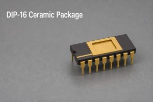
A DIP-16 ceramic package is a 16-lead, through-hole integrated-circuit package with two parallel rows of eight pins and a ceramic body. Engineers choose it when the device specification calls for ceramic construction, controlled sealing, thermal stability, long-term storage performance, or a qualified high-reliability package.

The name alone does not define every mechanical dimension or reliability grade. Lead pitch is commonly 2.54 mm, but body width, row spacing, lead shape, lid material, seal method, finish, temperature rating, and screening depend on the exact manufacturer drawing and part number. PCB designers and buyers should therefore treat the package drawing—not a generic DIP library—as the controlling source.

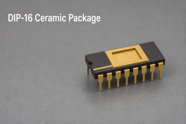
Dark ceramic DIP-16 package with a gold lid area and two rows of gold-plated leads

What Is a DIP-16 Ceramic Package?

A DIP-16 ceramic package is a ceramic dual in line package with 16 external leads arranged as eight pins per side. The ceramic body protects the semiconductor die, while internal bond wires connect the die pads to the external lead system. A lid and sealing structure close the cavity in cavity-style packages.

The query what is dual in line package refers to the broader rectangular package form with two parallel lead rows. DIP describes that form factor; the number 16 gives the total pin count. Ceramic describes the body or package construction. A buyer searching for a ceramic dual in line package may still need to specify whether the device uses a metal-lid side-brazed structure, a glass- or frit-sealed CERDIP construction, or another vendor-defined ceramic package.

For a broader overview of package families, see our guide to IC package types and PCB footprints. The new design decision here is narrower: whether the exact 16-lead ceramic device drawing is compatible with the PCB footprint, assembly process, inspection plan, and procurement specification.

How Do DIP-16, CDIP-16, and CERDIP-16 Terms Differ?

DIP-16 defines the lead arrangement and pin count, while CDIP and CERDIP usually identify ceramic dual in-line package constructions. Vendor terminology is not perfectly uniform, so the package code on the datasheet must be tied to its mechanical outline and sealing description.

Term What It Identifies What Still Needs Verification
DIP-16 Two parallel rows with 16 total leads Body material, width, row spacing, seal, finish, and qualification
CDIP-16 A 16-lead ceramic dual in-line package designation Side-brazed or other construction, lid and seal system, exact case outline
CERDIP-16 A 16-lead ceramic DIP, often associated with a ceramic and glass- or frit-sealed construction Manufacturer-specific seal process, moisture rating, temperature range, and screening
PDIP-16 A 16-lead molded plastic DIP It is not a drop-in ceramic substitute unless the electrical and mechanical specifications match

Ceramic does not automatically mean hermetic, military-qualified, radiation-hardened, or suitable for every high-temperature application. Those claims require device-level documentation. The safest procurement wording names the manufacturer, full part number, package designator, drawing revision, lead finish, temperature grade, and any required screening or qualification.

DIP 16 Package Dimensions

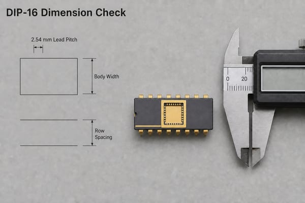
The most common dip 16 package dimensions start with a 2.54 mm lead pitch and two rows of eight pins, but there is no single universal body outline. A 300 mil ceramic DIP family commonly uses approximately 7.62 mm nominal row spacing, while the body length, shoulder width, lead thickness, seating plane, and tolerances vary by package drawing.

Dimension or Feature Common Starting Point Design Action
Lead count 16 total, eight per side Confirm numbering and pin-1 orientation on the device drawing
Lead pitch 2.54 mm nominal is common Use the drawing tolerance, not only the nominal library value
Row spacing 7.62 mm nominal is common for a 300 mil style Verify whether the drawing controls lead centers, body width, or both
Body length and width Vendor- and construction-dependent Build the courtyard and socket clearance from maximum dimensions
Lead section Rectangular or formed lead geometry Calculate the finished hole from maximum lead size and assembly allowance
Seating plane Direct seating or controlled standoff Check underside clearance, cleaning access, and mechanical stress

Generic dip package dimensions are suitable for an early concept only. Before releasing Gerbers, compare the PCB footprint with the exact package drawing from the approved component manufacturer. Microchip publishes ceramic DIP drawings in its packaging specification, while Renesas provides a specific 16-lead ceramic metal-seal package drawing. These examples also show why one generic body-length value should not be applied to every source.

Quality engineer measuring a ceramic package body against its mechanical drawing

Which Materials, Lead Finishes, and Seals Are Used?

Ceramic DIP construction usually combines an alumina-based body, a conductive internal metallization system, a semiconductor die, bond wires, external alloy leads, and a lid or sealing layer. The exact materials affect thermal expansion, wire-bond compatibility, corrosion resistance, solderability, and storage requirements.

  • Ceramic body: Provides dimensional stability, electrical insulation, and a low-permeability enclosure compared with molded plastic.
  • Lead system: Iron-nickel or iron-nickel-cobalt alloys are common starting points, but the drawing or material declaration controls.
  • Lead finish: Gold, nickel/gold, tin-based, or other finishes may be supplied. The selected finish must match soldering, wire-bond, storage, and compliance requirements.
  • Bond wire: Gold or aluminum wire may connect the die to package pads, depending on the device process.
  • Die attach: Eutectic, solder, or adhesive attachment may be used according to thermal and reliability needs.
  • Seal: Metal-lid, brazed, glass, or frit-based structures are possible. Hermeticity must be confirmed from the package specification and test documentation.

Finish compatibility deserves special attention in repair and long-storage programs. Gold-plated leads, for example, may require a controlled gold-removal decision under the applicable assembly specification. Procurement should not substitute a different finish without engineering approval.

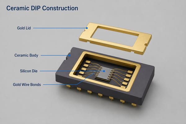
How Do Die Attach, Wire Bonding, and Hermetic Sealing Work?

The die is attached inside the ceramic cavity, bond wires connect it to metallized package pads, and the lid closes the cavity. In a hermetic design, the seal system is intended to limit gas and moisture ingress, but the actual performance depends on the construction, process controls, and verified leak-test requirements.

  1. The ceramic base receives its metallized conductors and external lead system.
  2. The semiconductor die is attached to the die pad using the specified material and cure or bonding process.
  3. Wire bonds connect die pads to the package terminals.
  4. Visual inspection checks die placement, bond placement, contamination, and obvious mechanical defects.
  5. The lid is sealed with the specified metal, glass, frit, or related sealing process.
  6. Electrical, seal, dimensional, and screening tests are applied as required by the device specification.
Exploded ceramic integrated circuit package showing the lid, sealing ring, die cavity, and gold wire bonds

A ceramic enclosure protects the die; it does not eliminate electrical overstress, electrostatic discharge, cracked bonds, lid damage, corrosion, or assembly-induced failure. Device handling and board assembly controls remain necessary.

Which Package Drawings and Standards Should Engineers Check?

The controlling documents are the approved component datasheet, manufacturer package drawing, purchase specification, and applicable assembly standard. JEDEC outlines and military package case descriptions can help identify a family, but they do not replace the part-specific drawing.

  • Mechanical package drawing: Lead pitch, row spacing, body envelope, lead section, seating plane, and tolerances.
  • Device datasheet: Pinout, orientation, temperature range, electrical ratings, handling, and soldering limits.
  • Package or case designation: JEDEC- or MIL-style references when the manufacturer provides them.
  • Assembly requirements: The contractually specified edition of IPC J-STD-001, IPC-A-610, or customer workmanship criteria when applicable.
  • Material and compliance records: Lead finish, substance declaration, storage condition, moisture or hermetic data, and traceability required by the purchase order.

Do not copy a footprint solely because two devices are both called CDIP-16. Match the full package designator and drawing dimensions. Also confirm whether the document shows the bottom view or top view before assigning pin numbers.

Where Are DIP-16 Ceramic Packages Used?

DIP-16 ceramic packages appear in equipment that values robust packaging, extended temperature options, long-term device storage, socketability, or qualified legacy components. Actual suitability comes from the complete device specification rather than the ceramic body alone.

  • Industrial controls and instrumentation built around mature through-hole architectures.
  • Test fixtures, development systems, and socketed devices that require replacement or programming access.
  • Aerospace, defense, or high-reliability electronics when the exact device has the required qualification and screening.
  • High-temperature or harsh-environment electronics when electrical ratings, package materials, and board design support the operating condition.
  • Maintenance and redesign programs that must support an approved legacy package.

A plastic PDIP may share a similar footprint, but it is not automatically an acceptable replacement. Engineers must compare electrical performance, temperature rating, sealing, lead finish, mechanical envelope, qualification, lifecycle status, and system-level reliability.

What Should Engineers Check When Designing the PCB Footprint?

The PCB footprint should be built from maximum and minimum package dimensions, not from a nominal pin grid alone. The two lead rows must align without forcing the ceramic body or bending leads during insertion.

  • Use two rows of eight plated through holes and mark pin 1 clearly on assembly and silkscreen layers.
  • Set hole size from the maximum lead cross-section, insertion allowance, plating thickness, and fabrication tolerance.
  • Choose annular rings that meet the board class, copper weight, drill tolerance, and rework needs.
  • Provide enough courtyard for the maximum body, socket, extraction tool, adjacent components, and inspection access.
  • Check copper clearance around each hole and decide whether thermal reliefs are appropriate for solderability and current.
  • Keep routing and components away from the body area when a socket, standoff, or underside cleaning access is required.
  • Review board thickness and hole aspect ratio if the assembly uses wave or selective soldering.

Our through-hole PCB design guide explains how finished-hole control, annular rings, component clearance, and assembly method affect manufacturability. Those checks are especially important when a brittle ceramic body must fit without lead stress.

How Should a DIP-16 Ceramic Package Be Assembled and Inspected?

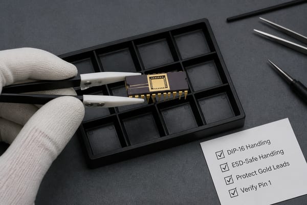
Assembly should protect the package from electrostatic discharge, lead deformation, excessive insertion force, thermal shock, and incompatible cleaning. A ceramic package may tolerate demanding environments in service, yet it can still crack or suffer seal and bond damage if handled poorly.

  1. Incoming inspection: Verify the part number, package code, date or lot traceability, lead finish, seal condition, pin-1 mark, and lead coplanarity.
  2. Footprint fit check: Test a representative component or approved gauge before production. Never force the two rows into a mismatched footprint.
  3. ESD-safe insertion: Align pin 1, support the board, and insert the device or socket evenly.
  4. Solder-process control: Apply the component manufacturer’s temperature and time limits. Tune wave, selective, or hand soldering to the board thermal mass.
  5. Cleaning: Confirm that the component, socket, markings, and seal are compatible with the cleaning chemistry and process.
  6. Post-solder inspection: Inspect fill, wetting, bridging, insufficient solder, lifted lands, contamination, lead damage, body cracks, and orientation.
  7. Electrical verification: Perform the required continuity, programming, functional, or system test after visual acceptance.
Gloved operator handling a dark ceramic DIP-16 package with ceramic-tip tweezers on an ESD-safe work surface

A socket can reduce heat exposure and simplify replacement, but it adds contact resistance, height, cost, and another mechanical interface. Direct soldering removes the socket interface but makes replacement and rework more difficult. Select the method from serviceability, vibration, reliability, and lifecycle requirements.

What Common Failures Should Designers and Buyers Prevent?

The most preventable failures come from wrong footprints, forced leads, incorrect orientation, unsupported substitutions, poor storage, and uncontrolled soldering. Ceramic construction does not compensate for a mismatched assembly process.

Failure Mode Likely Cause Prevention
Lead bending or package stress Incorrect row spacing or forced insertion Verify the drawing, use a fit check, and control lead forming
Wrong circuit behavior Pin-1 orientation or pinout error Align schematic, footprint, silkscreen, assembly drawing, and inspection program
Weak or open solder joint Wrong hole size, oxidized finish, insufficient heat, or poor flux access Control finished holes, storage, solder profile, and joint inspection
Body or seal damage Mechanical impact, clamping force, thermal shock, or aggressive rework Use protected handling, supported insertion, and approved temperature limits
Field reliability mismatch Assuming ceramic equals qualified or hermetic Require the exact device grade, test evidence, and approved source
Early redesign or shortage Obsolescence or single-source package dependency Check lifecycle status and qualify alternatives before production need becomes urgent

What Information Should Buyers Include in a DIP-16 RFQ?

A useful RFQ identifies both the component and the board-assembly requirements. “DIP-16 ceramic” alone leaves too many variables open and can lead to an electrically correct but mechanically or commercially unsuitable substitution.

  • Manufacturer and complete component part number.
  • Package designator and controlled mechanical drawing revision.
  • Required temperature grade, qualification, screening, and traceability.
  • Lead material and finish, including any solderability or gold-removal requirement.
  • Approved alternates and the engineering change process for substitutions.
  • Gerber or ODB++ data, drill files, fabrication drawing, assembly drawing, BOM, and centroid data where applicable.
  • Direct solder or socket requirement, board quantity, prototype and production volumes, and test scope.
  • Packaging, storage, date-code, shelf-life, and counterfeit-avoidance requirements.

If the component is obsolete or allocation-sensitive, ask for source traceability and do not authorize an alternate based only on the words “DIP-16.” Pinout, speed grade, temperature range, package seal, finish, dimensions, and qualification must all be reviewed.

FAQ About DIP-16 Ceramic Packages

1. Is every DIP-16 ceramic package hermetic?

No. Ceramic describes the package material or construction, while hermeticity is a verified package performance requirement. Confirm the seal type, package specification, leak-test requirement, and device documentation.

2. What Is a Dual In Line Package, and Does Every DIP-16 Use a 2.54 mm Lead Pitch?

A 2.54 mm pitch is common for standard dual in-line packages, but the approved mechanical drawing remains the authority. Do not release a footprint from the package name alone.

3. Can a ceramic DIP-16 replace a plastic PDIP-16?

Only after engineering verifies pinout, electrical ratings, timing, temperature range, body and lead dimensions, finish, qualification, and system requirements. A shared pin count does not make two devices equivalent.

4. Should a ceramic DIP-16 be socketed or soldered directly?

Use a socket when replacement, programming, or thermal isolation during assembly is important. Direct soldering may be preferable when contact interfaces, height, vibration, or cost are more critical. Evaluate the complete operating environment.

5. How is the correct plated-hole diameter selected?

Start with the maximum lead cross-section, then add insertion allowance and account for plating and drill tolerances. The PCB fabricator and assembler should review the finished-hole requirement together.

6. What should be inspected after soldering?

Check orientation, body and seal condition, lead damage, solder wetting, hole fill, bridging, contamination, lifted pads, and board damage. Complete the electrical or functional test required by the product plan.

How Can EBest Circuit Support a DIP-16 PCB Assembly?

A reliable DIP-16 assembly starts with the correct component drawing, plated-hole design, solder method, inspection criteria, and substitution controls. At EBest Circuit, we can review your PCB fabrication and PCBA package for through-hole or mixed-technology production. Send us the Gerber files, drill data, BOM, assembly drawing, package drawing, quantities, and test requirements so our engineering team can evaluate manufacturability and prepare a quotation at sales@bestpcbs.com.

You may also like

Modular PCB Design for Scalable Multi-Board Systems

August 25th, 2026

modular PCB design divides an electronic system into defined functional boards or circuit blocks that can be developed, verified, replaced, and reused with controlled interfaces. It is useful when a product family needs several configurations, when different teams work in parallel, or when one subsystem is likely to change before the rest of the product.

The method does not make a system reliable by itself. A module boundary adds connectors, return-path transitions, power-entry conditions, mechanical tolerances, and version-control decisions. The design succeeds only when those interfaces are treated as engineering specifications rather than convenient pin headers added near the end of layout.

Modular PCB Design with a main board and interchangeable functional PCB modules

What Is Modular PCB Design?

Modular PCB design is a system architecture in which each module has a defined function, a controlled interface, and a clear verification boundary. A module might handle power conversion, processing, sensing, motor control, communication, data acquisition, or a user interface.

Modularity can exist at two levels:

  • Logical modularity: functional blocks remain on one PCB but use separate schematic sheets, layout zones, power domains, and test boundaries.
  • Physical modularity: functions are placed on separate boards connected by mezzanine connectors, card-edge contacts, cables, backplanes, or soldered modules.

A product does not need multiple boards to benefit from modular thinking. Even a single-board design becomes easier to review when power, analog, digital, RF, and safety-related sections have explicit boundaries. Physical separation is justified when it improves reuse, serviceability, configuration control, parallel development, enclosure fit, or risk isolation enough to offset the added interconnect cost.

Which Modular PCB Architecture Fits the System?

The best architecture follows the product’s service model, signal bandwidth, available volume, mechanical envelope, and expected upgrade path. It should not be chosen only because stacked boards look compact.

Architecture Best Fit Main Constraint
Motherboard with daughtercards Products with optional or replaceable functions Connector alignment, stack height, and local support
Backplane with plug-in cards Expandable industrial, communications, and test systems Shared power, bus loading, card guides, and airflow
Stacked boards Compact embedded devices with limited footprint Thermal shadowing, inspection access, and tolerance stack
Cable-linked boards Modules placed around an enclosure or moving assembly Cable loss, EMI, strain relief, and connector retention
Soldered castellated module Reusable RF, sensing, or processing subassemblies Reflow profile, pad geometry, rework, and test access

For a deeper look at stacked structures and their assembly implications, compare this architecture decision with our PCB on PCB design guide. That physical stacking decision is only one part of a complete modular system.

Comparison of motherboard daughtercards, backplane plug-in cards, and stacked PCB architectures

How Should Functional Boundaries Be Defined?

Start with functions and failure domains, not arbitrary board outlines. A useful boundary minimizes the number of signals crossing between modules while keeping each module independently understandable and testable.

Review each proposed boundary against these questions:

  • Does the module perform one coherent function with clear inputs and outputs?
  • Can it be powered, programmed, and tested without the complete product?
  • Are high-current paths, precision analog signals, clocks, RF feeds, or safety barriers being forced through an unnecessary connector?
  • Will the module be reused across enough products or variants to justify interface control and separate lifecycle management?
  • Can a failed module be isolated without replacing a large portion of the system?

Create an interface control document before detailed layout. It should identify every pin, direction, electrical level, power state, allowable load, timing requirement, reference ground, pull-up ownership, default state, reserved position, mating sequence, and compatibility rule. The document should also state which module revision is compatible with each host-board revision.

Module interface definition separating power, ground, high-speed data, control, and reserved contacts

How Should a Modular PCB Connector Be Specified?

A modular PCB connector must be selected as an electrical, mechanical, assembly, and service component at the same time. Pitch and pin count alone are not enough.

  • Electrical: current per contact, contact resistance, voltage rating, ground-to-signal ratio, shielding, and high-speed performance.
  • Mechanical: mating height, insertion force, retention, alignment features, durability cycles, keying, and tolerance to vibration or shock.
  • Assembly: SMT or through-hole termination, coplanarity, reflow compatibility, paste design, inspection access, and repair method.
  • Lifecycle: availability, second-source strategy, connector revision control, and the consequence of obsolescence.

Place ground contacts beside sensitive or fast signals when the connector system supports it. Avoid assigning every ground pin to one end of a long connector because that can force return current to take a larger loop. For removable modules, add polarization or mechanical keying so an incompatible card cannot be inserted in the wrong orientation.

How Do Signal Integrity and Return Paths Cross Module Boundaries?

Every connector is an impedance discontinuity. The signal sees PCB traces, pads, vias, contacts, another set of pads and vias, then a second PCB. At low edge rates this transition may be forgiving; at high edge rates it can create reflection, loss, crosstalk, mode conversion, and timing error.

Control the complete channel rather than checking each board in isolation:

  • Route fast signals over continuous reference planes up to the connector launch.
  • Provide nearby ground contacts so return current can cross the same physical boundary.
  • Minimize stubs, unused connector branches, and unnecessary layer changes.
  • Keep differential pair geometry and skew controlled through both launches.
  • Include connector models, via models, and both PCB stackups in channel simulation when the data rate requires it.
  • Define whether termination is located on the source module, destination module, or backplane.

Our high-speed digital PCB guide explains controlled impedance, differential pairs, vias, crosstalk, and return-path planning in more detail.

Signal integrity and power integrity controls across a board-to-board module boundary

How Should Power Be Distributed Across Modular Circuit Boards?

Power architecture should be defined before connector pinout. Decide whether the host distributes raw input power, regulated system rails, or both. A raw-bus approach gives each module local regulation and fault isolation, while shared regulated rails can reduce duplicate circuitry but make voltage drop, transient loading, and compatibility more sensitive.

For every rail crossing modular circuit boards, document:

  • Nominal voltage, tolerance, continuous current, peak current, and startup current.
  • Contact allocation, current derating, acceptable voltage drop, and temperature rise.
  • Power-up and power-down sequence, reset behavior, and back-powering risks through signal pins.
  • Local input capacitance, decoupling, bulk storage, and load-transient limits.
  • Fuse, current-limit, reverse-polarity, overvoltage, and fault-containment strategy.
  • Whether live insertion is prohibited or intentionally supported.

Do not assume a removable card is hot-swappable. Live insertion may require staggered contacts, pre-charge, inrush control, power-good logic, and firmware behavior that prevents undefined bus activity. If the product is serviced only when powered off, say so clearly in the interface and service documentation.

Which Mechanical and Thermal Constraints Need Early Control?

A modular electrical design can fail at integration because the boards do not mate reliably, the enclosure loads the connector, or one card blocks airflow to another. Use the mechanical model early enough to influence board outline and placement.

  • Set connector location, mating height, board spacing, and allowable positional tolerance as shared dimensions.
  • Add guide pins, card guides, standoffs, screws, latches, or enclosure features when the connector should not carry the full mechanical load.
  • Check keep-outs around extraction paths, fasteners, cable bends, test probes, and rework tools.
  • Model component height on both sides of every board, including manufacturing tolerances.
  • Review heat-source alignment, airflow blockage, heatsink access, and thermal coupling between stacked modules.
  • Define the expected insertion cycles and service environment before choosing a connector family.

Mechanical reference points must match across the PCB outline, assembly drawing, enclosure model, and connector drawing. Small coordinate or revision errors can create a system-level interference even when each individual board passes inspection.

How Should Each Modular PCB Board Be Prepared for Manufacturing?

Each modular PCB board needs its own buildable data package plus one system-level document that connects the revisions. Reusing a circuit block does not mean reusing an old manufacturing package without checking its current components, stackup, footprint data, and interface revision.

Before release, apply the same fabrication and assembly discipline to every module:

  • Gerber or approved intelligent data, NC drill files, board outline, and fabrication drawing.
  • Stackup, controlled-impedance requirements, material, copper, finish, thickness, and tolerances.
  • BOM, centroid data, assembly drawing, polarity notes, approved substitutions, and do-not-fit variants.
  • Connector part numbers, mating orientation, stack height, keep-outs, and inspection requirements.
  • Programming files, module serial or revision marking, test procedure, and pass/fail limits.

Run a PCB design for manufacturability review on each board and then repeat the review at the system level. The second pass catches problems that a board-only check misses, such as inaccessible connectors, blocked test points, conflicting revisions, and assembly-order constraints.

How Should a Modular PCB System Be Tested?

A modular PCB system should be verified in layers: module test, interface integration test, and complete system test. Passing a module-level functional test does not prove that the connector channel, shared power network, firmware handshake, enclosure, or thermal environment will work after integration.

  1. Test each module independently. Verify its power input, outputs, communications, programming, protection, and boundary conditions.
  2. Use known-good counterparts. A golden host board or golden module helps isolate whether a failure follows the module or the interface.
  3. Test every interface state. Include startup, reset, sleep, communication loss, overload, missing module, incorrect revision, and permitted insertion or removal conditions.
  4. Validate the complete assembly. Measure signal margins, rail behavior, temperatures, EMI-sensitive conditions, and performance inside the final enclosure.
  5. Preserve traceability. Record board revision, firmware version, BOM variant, module serial number, and test result as one system configuration.

Test points should remain accessible before and after modules are installed. If a fixture cannot contact critical nets in the assembled state, provide a dedicated test connector, boundary-scan path, built-in self-test, or another agreed diagnostic interface.

Module test, integration test, and complete modular PCB system test workflow

When Does a Modular Design Add Cost or Risk?

Modularity is not automatically cheaper. It can reduce redesign and service cost while increasing unit hardware cost. The correct comparison uses total product and lifecycle impact, not the PCB price alone.

Potential Benefit Possible Added Cost or Risk
Reuse of validated functions Interface documentation and compatibility validation
Parallel development More coordination, revision control, and integration testing
Replaceable or upgradeable modules Connectors, retention hardware, enclosure volume, and service access
Fault isolation Extra protection, diagnostic circuitry, and test fixtures
Product configuration from common blocks Variant management, inventory, and end-of-life coordination

A monolithic board may be better when the product is small, cost-sensitive, built in one stable configuration, and dominated by short high-speed or high-current paths. A modular architecture becomes stronger when the product family changes frequently, field replacement matters, teams can truly work in parallel, or validated functions will be reused across several products.

FAQ About Modular PCB Design

  • Is a modular PCB the same as a daughterboard? No. A daughterboard is one physical module type. Modular design also includes backplanes, stacked boards, cable-linked assemblies, soldered modules, and logical blocks on one PCB.
  • Can a modular PCB improve repairability? Yes, when failed functions can be diagnosed and replaced independently. Repairability still depends on accessible connectors, spare-module control, service documentation, and safe replacement procedures.
  • Are board-to-board connectors suitable for high-speed signals? They can be, but the connector, launches, vias, reference contacts, stackups, and complete channel must meet the interface bandwidth and signal-integrity requirements.
  • Should every module use the same connector? Not necessarily. Standardization helps reuse, but power, high-speed, RF, safety, mechanical, and environmental requirements may justify different connector families.
  • What files are needed to quote a multi-board assembly? Provide the fabrication package for every PCB, BOM and placement data for every assembly, mechanical drawings, the module/interface definition, test requirements, quantities, variants, and one revision matrix for the full system.

The most important rule is to treat modular PCB design as a controlled system architecture. Reusable boards are valuable only when their electrical, mechanical, firmware, manufacturing, and test interfaces remain explicit.

How Can EBest Circuit Support Your Modular PCB Project?

At EBest Circuit, we support PCB fabrication, component sourcing, PCBA assembly, DFM review, and agreed inspection or functional testing for multi-board electronic products. We can review the individual module files together with connector orientation, stack height, controlled-impedance needs, assembly sequence, and system test access before the build is released.

For a useful engineering review and quotation, send the Gerber or ODB++ data for each board, NC drill files, stackups, fabrication drawings, BOMs, placement files, assembly drawings, connector specifications, quantities, revision matrix, and test requirements. Our PCB manufacturing and assembly guide can help you organize that package.

Email sales@bestpcbs.com with your project files and system constraints. We will review the manufacturing and assembly scope against the actual module architecture instead of treating each PCB as an unrelated order.

You may also like

EBest Circuit: Your One-Stop PCB & PCBA Manufacturing Partner

August 24th, 2026

EBest Circuit is a one-stop PCB and PCBA manufacturing partner founded in 2006. We support bare PCB fabrication, component sourcing, SMT and through-hole assembly, testing, prototype builds, and volume production for global electronics projects.

If you are evaluating a PCB supplier for a new project, send us your Gerber files, BOM, stack-up, quantity, and testing requirements. Our engineering team can review the manufacturing package before quotation and help identify process risks early.

Item EBest Circuit Support
Core services PCB fabrication, component sourcing, PCBA assembly, testing, box-build support
Project stage Prototype, small-volume build, and volume production
Manufacturing support Shenzhen, China and Vietnam manufacturing support
Technical review DFM, stack-up, material, copper weight, impedance, assembly and test review
Typical files for review Gerber, drill, stack-up, BOM, pick-and-place, drawings and test requirements
EBest Circuit one-stop PCB and PCBA manufacturing partner hero image

Who Is EBest Circuit?

EBest Circuit is a PCB and PCBA manufacturing partner for electronics teams that need more than a bare-board supplier. We help customers move from early design review to PCB fabrication, component sourcing, assembly, inspection, and production planning.

Our work covers conventional rigid PCB projects as well as more specialized requirements such as HDI, RF/high-frequency materials, heavy copper, metal-core PCB, ceramic PCB, flexible PCB, rigid-flex PCB, and turnkey PCBA. For each project, we review the actual files instead of treating a single capability number as a universal answer.

What Can We Build?

We support both standard PCB technologies and project-specific builds that require engineering review. The best starting point is a complete manufacturing package, because layer count, material, copper weight, hole structure, board size, surface finish, assembly requirements, and testing all affect feasibility.

Product or Service Typical Support
Rigid PCB Single-sided, double-sided and multilayer rigid PCB fabrication
HDI PCB Fine features, laser blind/buried vias and high-density interconnect structures
RF / High-Frequency PCB Rogers, Taconic, PTFE, Isola, Nelco and other specified laminates
Heavy Copper PCB High-current and mixed-copper designs reviewed by stack-up and copper distribution
Metal-Core PCB Aluminum, copper and stainless-steel substrate options
Ceramic PCB Thin Film, DBC/DCB, DPC and AMB ceramic substrate technologies
Flexible PCB Single-, double- and multilayer FPC through our flexible PCB support path
Rigid-Flex PCB Combined rigid and flexible structures for compact electronic assemblies
PCB Assembly SMT, THT/DIP, mixed assembly, component sourcing and agreed testing
Box-Build Support PCB with cable, wire, enclosure or project-specific assembly requirements

For flexible PCB and rigid-flex projects, customers can also review our dedicated flexible PCB manufacturing resources at bestfpc.com. For ceramic substrate projects, our ceramic PCB information is available at bstceramicpcb.com.

Wide view of PCB manufacturing workshop with operators and inspection benches

How Do We Review PCB Manufacturing Capability?

PCB capability depends on the full construction, not only on one headline parameter. A 32-layer rigid PCB, a 20 oz heavy copper board, a 0.10 mm laser via design, and a special laminate project may each require a different review path.

Our current FR-4 process specification separates standard process ranges from special-process review. The table below summarizes key items customers often ask about during supplier evaluation.

Capability Standard Process Special Process / Review
FR-4 layer count 1-10 layers 10-32 layers
Inner copper 0.5-5 oz 5-20 oz
Outer copper 1-5 oz 5-20 oz
Laser blind/buried via 0.10 mm Project construction must be reviewed
Minimum finished mechanical hole 0.20 mm 0.15 mm
Through-hole aspect ratio Up to 8:1 Up to 10:1
Inner trace/space 4/4 mil at suitable copper 3/3 mil at suitable copper
Outer trace/space 4/4 mil at suitable copper 3/3 mil at suitable copper
Surface finishes OSP, HASL, ENIG, ENEPIG, immersion silver, immersion tin, hard gold and others Project dependent

These values should be used as an early screening reference. Final manufacturability still depends on the complete stack-up, panel size, copper distribution, finished thickness, tolerance, surface finish, quantity, and inspection requirements.

Why Do Engineers Work With Us?

Engineering teams work with us because many PCB problems are easier to solve before production starts. We review the design package early so customers can correct unclear specifications, high-risk stack-ups, component sourcing gaps, or testing assumptions before they become schedule and reliability problems.

  • Gerber and drill-file completeness review.
  • Stack-up, material and finished thickness review.
  • Copper weight, spacing and impedance discussion.
  • Hole, via, blind/buried via and HDI structure review.
  • Surface finish and solderability review.
  • BOM sourcing and component availability checks.
  • SMT, THT/DIP and mixed-assembly process review.
  • Inspection and functional-test planning.
  • Prototype-to-production transition support.

This approach is especially useful for HDI, RF PCB, heavy copper PCB, metal-core PCB, ceramic PCB, rigid-flex PCB, dense PCBA, BGA assembly, fine-pitch components and projects with formal inspection documentation.

PCB engineers reviewing layout and stack-up files during DFM review

How Do We Support PCB Materials and Special Technologies?

Material selection affects thermal behavior, signal performance, dimensional stability, assembly reliability, and cost. We help customers match material choices to the electrical, mechanical, thermal, and supply-chain needs of the project.

  • Low-Tg, mid-Tg and high-Tg FR-4.
  • Halogen-free FR-4 and selected high-temperature material options.
  • Rogers 4003, Rogers 4350, Rogers 5880 and other RF laminate families.
  • Taconic, PTFE, Isola 370HR, Isola FR408HR and Nelco options.
  • Aluminum, copper and stainless-steel substrates for metal-core PCB.
  • Al2O3, AlN, ZrO2, Si3N4 and other ceramic substrate options by process type.
  • Flexible and rigid-flex materials for FPC and compact assemblies.

Material availability should be confirmed with the target thickness, copper type, layer structure, impedance target, quantity, and delivery requirement. For special laminates, we recommend confirming procurement before the layout is frozen.

How Do We Support Turnkey PCBA?

EBest Circuit can continue the project after bare-board fabrication, so customers do not need to coordinate separate PCB, component sourcing, and assembly suppliers for every build.

  • SMT assembly.
  • THT / DIP assembly.
  • Mixed SMT and through-hole assembly.
  • Component sourcing.
  • Customer-supplied components.
  • PCB with wire or cable assembly.
  • Box-build assembly.
  • Inspection and functional testing.

Customers can choose turnkey PCBA, consigned components, or hybrid sourcing. For turnkey projects, we handle PCB fabrication, component sourcing, assembly, and agreed testing. For consigned or hybrid builds, customers can supply controlled, programmed, allocated, or critical components while we support the remaining manufacturing scope.

PCBA assembly line with populated circuit boards moving through production

What Quality Certifications and Standards Support Our Work?

Quality documentation matters when a PCB or PCBA supplier is part of a formal approval process. EBest Circuit company materials list ISO 9001:2015, ISO 13485:2016, IATF 16949, AS9100D, UL, RoHS, REACH and FPC SGS documentation.

Certification scope can vary by product, process, manufacturing route, and customer requirement. If your project requires a specific IPC class, certificate package, quality document, material record, inspection plan, or customer audit, include it in the RFQ so we can confirm the applicable path before production.

Certification or Compliance Item Typical Relevance
ISO 9001:2015 General quality management
ISO 13485:2016 Medical-device-related quality management
IATF 16949 Automotive quality management
AS9100D Aerospace-related quality system requirements
UL / UL E502832 UL recognition and product documentation
RoHS / REACH Environmental compliance support
FPC SGS documentation Supporting documentation for flexible PCB projects

How Do We Control PCB and PCBA Quality?

Quality control is built across incoming inspection, fabrication, assembly, final inspection, and shipment. The right inspection plan depends on the board type, component density, end application, and customer requirements.

For PCB fabrication, inspection and measurement may include:

  • AOI.
  • Electrical testing.
  • Flying probe testing.
  • Impedance testing.
  • Copper-thickness measurement.
  • Microsection inspection.
  • Hole-diameter measurement.
  • Dimensional measurement.

For PCBA production, inspection may include SPI, AOI, X-ray, first-article inspection, functional testing, and project-specific tests. A simple SMT assembly does not need the same test plan as a dense PCBA with BGA, fine-pitch ICs, programmed devices, firmware loading, or critical functional requirements.

Engineer inspecting assembled printed circuit boards under microscope

What Testing and Inspection Methods Are Available?

Each test method is selected to control a specific manufacturing risk. Customers should specify required testing, fixtures, firmware, procedures, expected outputs, and pass/fail criteria where applicable.

Inspection / Test Main Purpose
AOI Checks visible PCB or assembly defects
Flying Probe / E-Test Detects opens and shorts
SPI Checks solder-paste deposition
X-Ray Inspects hidden solder joints such as BGA connections
Impedance Test Verifies controlled-impedance structures
Microsection Examines plated holes and internal construction
Copper Thickness Test Confirms copper thickness
Dimensional Measurement Checks mechanical dimensions
FAI / First Article Verifies the initial build before continuing
Functional Test Confirms agreed electrical or functional behavior
XJTAG Supports applicable boundary-scan or test requirements

Not every project needs every inspection method. The most efficient test plan is the one that matches the real product risk.

What Lead Time Should You Expect?

Lead time depends on layer count, material availability, copper thickness, board complexity, component sourcing, inspection requirements, testing scope, and production quantity. Prototype and volume production schedules should be reviewed separately.

Reference FR-4 prototype lead times in company materials include:

  • Single-layer PCB: 3-4 days.
  • 2-layer PCB: 4-6 days.
  • 4-6 layer PCB: 6-10 days.
  • 8-layer PCB: 10-14 days.
  • 10-layer PCB: 14-18 days.
  • 1+N+1 / 2+N+2 HDI: about 2.5-3.5 weeks.

For PCBA projects with customer-supplied components, reference prototype assembly lead times include about 1 week for components >=0402 without DIP, about 1-2 weeks for components >=0402 with DIP, about 1-2 weeks for components <=0201 without DIP, and about 1.5-2 weeks for components <=0201 with DIP. BOM purchasing can add time, especially when components are unavailable, allocated, obsolete, or long-lead.

What Should You Send for Engineering Review?

The fastest way to evaluate a PCB or PCBA project is to send the actual files and requirements. Partial files are useful at the early design stage, but a complete package gives a more reliable quotation and manufacturing plan.

For bare PCB review, send:

  • Gerber or ODB++ files.
  • NC drill files and drill table.
  • Stack-up and finished board thickness.
  • Material, copper weight and surface finish.
  • Impedance, via and tolerance requirements.
  • Quantity and target delivery date.
  • Required IPC class, certificates or inspection records.

For PCBA review, also send:

  • BOM.
  • Pick-and-place file.
  • Assembly drawing.
  • Component sourcing preference.
  • Programming requirements.
  • Functional-test requirements.
  • Expected prototype and production quantity.

If the design is still under development, send the files you already have. We can identify which specifications need to be confirmed before production.

Finished PCB and PCBA boards packed in anti-static bags for shipment

FAQ About Working With EBest Circuit

Can EBest Circuit support both PCB fabrication and PCBA assembly?

Yes. We support PCB fabrication, component sourcing, SMT assembly, THT/DIP assembly, mixed assembly, inspection, functional testing, and selected box-build requirements.

Can you review files before quotation?

Yes. Send Gerber files, drill files, stack-up, BOM, pick-and-place data, drawings, quantities, and test requirements. We can review manufacturability before quotation.

Can customers supply their own components?

Yes. Customers may choose turnkey PCBA, consigned components, or hybrid sourcing. Hybrid sourcing is useful when customers want to control critical ICs or programmed devices.

Can you support prototype builds before production?

Yes. We support prototypes, small-volume builds, and volume production. A project can move through prototype review, design updates, pilot production, and larger production batches.

Can customers arrange a factory audit?

Yes. Customers can arrange an audit as part of supplier qualification. Share the audit checklist, scope, preferred manufacturing site, and proposed date in advance.

What if a PCB is outside the standard process window?

Send the files for engineering review. Special-process items such as 3/3 mil features, 0.15 mm finished holes, high copper weight, more than 10 FR-4 layers, unusual thicknesses, or 10:1 aspect ratio need to be reviewed with the complete stack-up.

Start Your PCB or PCBA Project With EBest Circuit

If you are evaluating EBest Circuit as your PCB and PCBA manufacturing partner, send us the project data you already have. We can review the files, confirm the manufacturing path, raise technical questions, and prepare a quotation based on the actual build.

For bare PCB projects, send Gerber or ODB++ files, stack-up, material, copper weight, quantity, surface finish, and any inspection requirements. For PCBA projects, add the BOM, pick-and-place file, assembly drawing, sourcing preference, programming needs, and functional-test requirements.

Send your PCB or PCBA files to sales@bestpcbs.com for engineering review and quotation.


You may also like

Fiber Optic FPV Drones PCB Design and Manufacturing Guide

August 24th, 2026

A fiber optic fpv drones PCB connects the flight controller, camera or video processor, optical transceiver, power regulation, sensors, and motor-control interfaces in a compact airborne electronics system. The fiber carries optical data, but the PCB still has to manage high-speed electrical signals, switching noise, heat, vibration, connector stress, and strict weight limits.

The design should therefore be treated as a coordinated set of signal, power, mechanical, and manufacturing decisions. This guide focuses on the PCB and PCBA engineering needed for lawful industrial, inspection, research, and communications applications. Exact data rates, environmental limits, interfaces, and acceptance tests must be defined for each project.

Fiber Optic FPV Drones PCB with optical transceiver, flight controller, and fiber interface

What Is a Fiber Optic FPV Drones PCB?

A fiber optic FPV drones PCB is the board-level platform that routes control and video data between the drone electronics and an optical communication module. It may be one integrated assembly or several boards connected as a flight-control stack, camera board, optical-interface board, power board, and electronic speed controller system.

The optical fiber does not carry electrical power to the aircraft. A battery and local regulators still power the processor, sensors, camera, transceiver, and other loads. The PCB must keep those rails stable while motors and switching converters create rapid current changes. It must also preserve the electrical channel between the processor or video interface and the optical transceiver.

How Does a Fiber Optic FPV Drone Work?

A fiber-linked FPV platform converts electrical control and video data into optical signals, sends them through a lightweight fiber, and converts them back at the opposite end. The exact phrase fiber optic fpv drone how it works often leads readers to the link itself, but reliable operation also depends on the electronics around that link.

  1. The camera and sensors create video and flight data.
  2. The flight controller processes commands and sensor inputs.
  3. An electrical interface passes selected data to an optical transceiver or conversion module.
  4. The transceiver converts electrical data to light for transmission through the fiber.
  5. The ground-side unit performs the reverse conversion for the display and controller.

This arrangement can remove the primary control/video path from a conventional radio link, but it does not make the complete aircraft immune to every disturbance or failure. Power noise, damaged connectors, excessive fiber bending, processor faults, sensor errors, and mechanical stress can still interrupt the system.

Fiber optic FPV system architecture showing the drone PCB, optical link, and ground unit

Which Circuit Boards and Functional Blocks Make Up the System?

The system normally combines flight control, video, optical communication, power conversion, sensing, and motor interfaces. These functions can share one board, but separating them may simplify noise control, thermal management, service, and mechanical placement.

Board or Block Main Function PCB Design Focus
Flight controller Processes sensor data and generates control outputs Clean sensor power, stable clocks, short return paths, vibration-aware placement
Optical interface Converts electrical data to and from optical signals Differential routing, decoupling, connector retention, transceiver heat
Camera or video board Captures and conditions the FPV image stream High-speed interface integrity, low-noise power, compact interconnects
Power distribution and regulation Feeds logic, camera, optical module, and peripheral rails Current capacity, filtering, protection, thermal paths
ESC or motor interface Drives or commands the motors High-current loops, switching noise, MOSFET cooling, isolation from sensors

For a broader system comparison, our guide to the types of circuit boards used in drones explains how flight-control, power, camera, sensor, and communication boards divide the work.

What Makes an FPV Drone PCB Board Different?

An fpv drone pcb board must operate under tighter weight, space, vibration, and power-noise constraints than many stationary electronics. In a fiber-linked design, the optical interface adds another high-speed data path and a mechanically sensitive connection near a moving platform.

  • Mixed electrical environments: quiet sensors and high-speed data operate near motor switching and battery current.
  • Mass and balance: board dimensions, copper weight, connectors, shields, and the fiber assembly affect mechanical integration.
  • Limited cooling: airflow changes with enclosure, speed, board orientation, and nearby components.
  • Continuous movement: vibration can fatigue solder joints, connectors, cables, and unsupported components.
  • Service constraints: densely stacked boards need accessible test points and a clear replacement strategy.

These constraints should be set before schematic capture. Adding the optical module late can create blocked airflow, long data routes, poor connector access, or an unstable center of mass.

How Should an FPV Drone Controller PCB Handle the Optical Interface?

An fpv drone controller pcb should treat the optical transceiver as a high-speed electrical load with its own power, thermal, signal, and connector requirements. The fiber begins at the optical port; everything between the processor and that port is still an electrical PCB channel.

Start with the selected module datasheet and define its host interface, supply rails, peak current, reset behavior, clocking, connector, and thermal limits. Keep high-speed pairs short, maintain a continuous reference plane, and avoid stubs or unnecessary test pads. Place local decoupling close to supply pins and provide a low-inductance return path.

Connector orientation must be coordinated with the enclosure and fiber path. The optical connector or pigtail should not transfer repeated pull or twist directly into small solder joints. If the design uses a separate optical daughterboard, specify the board-to-board connector, retention method, mating cycle, and service access before layout.

Close view of an FPV drone optical interface PCB with transceiver and controlled routing

How Should Power Domains Be Separated from Motor Noise?

Power-domain planning should prevent motor and converter noise from disturbing the flight controller, camera, sensors, or optical interface. A single battery may feed every function, but that does not mean all loads should share the same unfiltered path.

  • Keep high-current battery and motor loops physically compact.
  • Separate sensitive regulators from switching nodes and hot power components.
  • Use the regulator vendor’s recommended input, output, and compensation layout.
  • Place high-frequency decoupling at the IC pins and bulk capacitance near load groups.
  • Do not split a reference plane beneath a high-speed signal simply to create visual separation.
  • Plan current return paths before routing signals between functional zones.

Power integrity should be checked during load transitions, not only at idle. The optical transceiver, processor, and camera may react differently to voltage droop or ripple. Test limits should come from the component datasheets and system specification rather than one generic ripple target.

Drone PCB power-domain layout separating motor current from flight-control and optical circuits

How Should High-Speed Video and Control Data Be Routed?

High-speed routes should be designed as transmission lines whose geometry, return path, vias, and connector launches are controlled from the processor to the optical module. The required impedance and matching tolerance depend on the actual electrical interface and component datasheets.

Practical layout checks include:

  • Define the stackup and target impedance with the PCB fabricator before final routing.
  • Keep differential-pair geometry consistent and avoid abrupt neck-downs.
  • Minimize stubs, layer changes, and unnecessary connector transitions.
  • Add nearby return vias when a high-speed pair changes reference layers.
  • Separate fast data from switching nodes, motor phases, and noisy clock sources.
  • Reserve test access that does not create an unacceptable discontinuity.

Our high-speed digital PCB design guide covers stackup, return paths, differential routing, vias, crosstalk, and power integrity in more detail. When waveform margin matters, an eye diagram can be combined with TDR, channel measurements, and functional testing under defined conditions.

What Does the Fiber Optic FPV Drone Cable Change Mechanically?

The fiber optic fpv drone cable adds bend-radius, strain-relief, routing, connector, and spool-integration requirements that must be resolved with the PCB and enclosure. The board should not become the mechanical anchor for an unsupported fiber path.

Define the minimum bend radius, connector or pigtail geometry, retention method, exit angle, and allowable movement from the chosen fiber and module documentation. Keep the path away from sharp board edges, propulsive components, hot surfaces, and service fasteners. If a separate spool or dispensing assembly is used, its loads should be carried by the mechanical structure rather than small PCB pads.

Mechanical review should also cover assembly sequence. A connector that is electrically correct may be unusable if it cannot be mated after the boards are stacked. A short flexible interconnect or daughterboard may improve serviceability, but it adds connectors and possible signal discontinuities that require validation.

Which PCB Stackup and Materials Fit the Design?

The stackup should be chosen from routing density, electrical interface speed, power-current needs, board thickness, weight, and manufacturing tolerance. There is no universal layer count or laminate for every fiber-linked drone controller.

Design Need Possible PCB Direction Decision Check
Compact controller with moderate routing density Multilayer FR-4 Reference planes, finished thickness, thermal margin, impedance feasibility
Fine-pitch processor or dense camera interface HDI construction when justified Escape routing, microvia structure, assembly yield, cost
Moving camera or constrained interconnect Flexible or rigid-flex circuit Bend zone, stiffener, dynamic-cycle requirement, connector reduction
Higher-current power section Localized heavier copper or separate power board Temperature rise, etching limits, weight, copper balance

Controlled impedance requires agreement on dielectric thickness, copper thickness, trace geometry, and material properties. Our impedance control PCB guide explains how design targets connect to fabrication and test coupons.

How Should Vibration, Heat, and Environmental Exposure Be Managed?

Reliability starts with the actual mounting, airflow, duty cycle, temperature, humidity, and vibration profile. A coating or stronger material cannot compensate for unsupported connectors, poor thermal paths, or components placed in high-strain areas.

  • Keep heavy components away from unsupported board edges where possible.
  • Use mounting-hole and keep-out geometry that avoids local copper or laminate stress.
  • Review connector retention and cable strain relief as part of the enclosure.
  • Provide copper area and thermal vias for regulators, processors, and power devices when the package guidance requires them.
  • Measure component temperatures in the real enclosure and operating airflow.
  • Select conformal coating or sealing only after checking connectors, sensors, optical surfaces, rework, and service requirements.

Board cleanliness matters if a coating will be applied. Flux residue or moisture trapped beneath a coating can create reliability problems instead of preventing them.

Which DFM and PCBA Checks Matter Before Production?

DFM and PCBA review should connect the schematic, layout, component data, mechanical model, and test plan before the first build. The review is most useful when it identifies risks that can still be changed.

  • Fabrication data: final Gerber or ODB++ data, drill files, stackup, controlled-impedance table, and board outline.
  • Assembly data: BOM with manufacturer part numbers, centroid file, polarity notes, approved substitutes, and special handling instructions.
  • Mechanical data: enclosure model, connector height, board stack spacing, mounting hardware, and fiber exit path.
  • Process checks: fine-pitch escape, solder-mask clearances, thermal-pad design, panelization, fiducials, and test-point access.
  • Supply checks: component lifecycle, optical-module availability, connector lead time, and traceable alternates.

If the design includes a dense image path, our camera PCB module guide provides related manufacturing and assembly considerations.

How Should the PCB Be Tested and Validated?

Validation should move from bare-board checks to assembled-board inspection and then to system testing under defined electrical and mechanical conditions. A board that powers on once has not yet demonstrated stable optical, control, sensor, and power performance.

Test Stage What It Checks Typical Evidence
Bare PCB Continuity, isolation, dimensions, holes, and controlled impedance when specified Electrical test record, dimensional inspection, impedance report or coupon data
PCBA inspection Placement, polarity, solder joints, bridges, voiding, and hidden connections AOI, X-ray where appropriate, visual inspection, reflow records
Power-up Rail sequence, current draw, ripple, reset, clocks, and thermal behavior Measured waveforms, current log, thermal measurements
Interface validation Camera, controller, sensor, and optical data paths Functional logs, error counters, waveform or channel measurements
System validation Operation in the intended enclosure, wiring, motion, and environment Approved test procedure and pass/fail report
Inspection and electrical testing of a fiber optic drone PCBA

FAQ About Fiber Optic FPV Drones PCB

  • Does the optical fiber replace every communication circuit?
    No. It can carry selected control and video data, but the system still needs processors, interfaces, sensors, local power, and possibly other links. The exact architecture depends on the product specification.
  • Does the PCB route optical signals as copper traces?
    No. Copper traces carry electrical signals to the optical transceiver. The transceiver converts those signals to light, which then travels through the fiber.
  • Is a high-frequency laminate always required?
    No. Material choice depends on the electrical interface, route length, loss budget, stackup, temperature, and fabrication tolerance. Multilayer FR-4 may be suitable for some designs, while others need a lower-loss construction.
  • Can the optical module share a regulator with the flight controller?
    Only if the load transients, ripple, sequencing, noise, and thermal limits remain within every component’s requirements. Separate filtering or regulation may be safer, but the decision should be verified by measurement.
  • What files are needed for PCB manufacturing and assembly review?
    Prepare fabrication data, drill files, stackup, impedance requirements, BOM, centroid file, assembly drawing, mechanical data, optical-module documentation, quantities, and the intended test plan.

How Can EBest Circuit Support Your Drone PCB Project?

A dependable fiber optic fpv drones PCB project needs the optical interface, flight-control electronics, power architecture, mechanics, and manufacturing data to agree before production. At EBest Circuit, we support PCB design review, PCB fabrication, component sourcing, PCBA assembly, impedance-related build requirements, and inspection for custom electronics projects.

Send your Gerber or ODB++ data, stackup, impedance table, BOM, centroid file, board dimensions, optical-module datasheet, quantities, mechanical constraints, and test requirements to sales@bestpcbs.com. We can review the manufacturing package and help prepare the board for prototype or production quotation.

You may also like

PCB Assembly France: Compare Suppliers and Get a Quote

August 24th, 2026

Choosing a supplier for PCB assembly France is not only a price decision. French engineers and buyers must protect design intent, component authenticity, build quality, delivery, and total landed cost—especially when comparing local, European, and overseas suppliers.

EBest Circuit (Best Technology) supports French PCB projects from its China-based PCB and PCBA factories. One commercial contact works with three engineers to coordinate DFM review, BOM optimization, PCB fabrication, component sourcing, assembly, inspection, and testing. The company supports prototypes and small batches as well as repeat production, including projects using heavy-copper, HDI, high-frequency, FPC, and rigid-flex PCB technologies.

Planning a PCB assembly project for France? Send your controlled PCB files, BOM, quantity, testing requirements, and delivery destination to sales@bestpcbs.com. EBest Circuit can review manufacturability and BOM risks before preparing an itemized quotation.

PCB assembly France
EBest Circuit’s SMT production environment supporting PCB assembly projects for French buyers.

What Should Buyers Expect from PCB Assembly France?

Expect a clearly defined manufacturing scope, named technical owners, controlled revisions, project-specific quality evidence, and a realistic landed delivery plan.

“PCB assembly France” can describe three sourcing models: production in France, production elsewhere in Europe, or an overseas supplier serving French customers. The best fit depends on the project—not the search phrase.

Before comparing prices, confirm who owns each part of the work:

  • Bare PCB fabrication and electrical testing.
  • Component procurement and approved substitutions.
  • SMT, through-hole, and manual assembly.
  • Programming, inspection, and functional testing.
  • Packaging, freight, customs, and import documentation.

For prototypes, fast engineering feedback and revision control often matter more than a small unit-price difference. For repeat orders, component continuity, process stability, traceability, and change control become more important.

EBest Circuit is an overseas option for French buyers, not a French factory or local legal entity. Buyers should therefore include international freight, customs, import responsibility, time-zone communication, and total landed lead time in the comparison.

PCB Assembly in Europe vs China: Which Model Fits French Buyers?

European production may fit projects that need frequent site access or very short transport. China-based production may fit projects that benefit from integrated PCB, component, assembly, and testing resources.

Buyer priorityEurope may fit whenChina may fit when
Engineering accessFrequent site visits are essentialOnline engineering reviews are sufficient
Supply scopeParts and processes are already localPCB, sourcing, PCBA, and test need coordination
CostProximity outweighs unit costRepeat-volume economics matter
Quality oversightOn-site review is preferredRemote records and traceability are accepted
DeliveryTransport time is the main constraintBuild time and sourcing efficiency matter more

Choose a nearby supplier when the design changes daily, physical collaboration is essential, or transport time dominates the schedule.

Consider a qualified China-based supplier when files are sufficiently mature, one team must coordinate several supply stages, or the project requires wider component-sourcing options. A hybrid model is also possible: keep unstable early builds close to the design team, then transfer a controlled package for repeat production.

In every model, compare the time from data release to usable boards at your facility—not only the factory build time.

PCB assembly France
Automated component placement on assembled PCBs during PCBA production.

What Files Are Needed for a PCB Assembly France Quote?

Send one revision-matched manufacturing package. Gerber files and a basic BOM are rarely enough for an accurate, production-ready quote.

Your package should include:

  • PCB data: Gerber or ODB++, drill files, board outline, stack-up, material, copper weight, finish, impedance, and special-process notes.
  • BOM: Manufacturer part numbers, quantities, reference designators, do-not-fit positions, approved alternates, and buyer-supplied parts.
  • Assembly data: Pick-and-place coordinates, rotations, board side, polarity, connector orientation, and assembly drawings.
  • Programming data: Firmware version, programming method, and verification instructions.
  • Quality requirements: IPC class if applicable, SPI, AOI, X-ray, electrical or functional test, report format, and acceptance limits.
  • Delivery requirements: Quantity, panelization preference, packaging, labeling, traceability, Incoterm, and destination.

Use the same revision identifier across every file. If the PCB data, BOM, centroid file, firmware, and drawings do not match, the supplier should issue an engineering query rather than guess.

EBest Circuit can provide a DFM pre-review and BOM risk or optimization list. The review may identify footprint conflicts, polarity questions, stencil risks, inaccessible test points, obsolete parts, long-lead components, and possible alternates. No substitute should be purchased without the buyer’s approval.

Before requesting a final price: Email the release package to sales@bestpcbs.com and ask EBest Circuit to separate confirmed parts, proposed alternates, unavailable items, tooling, testing, freight, and other one-time charges.

How Should French Buyers Compare PCB Assembly Quotes?

Compare equivalent scope and total landed project cost—not only the quoted price per assembled board.

Check these six areas in every quotation:

  • Bare PCB: Material, stack-up, finish, impedance, panelization, tooling, electrical test, and quantity.
  • Components: Exact part numbers, approved alternates, minimum purchasing quantities, excess material, and buyer-supplied parts.
  • Assembly: SMT sides, through-hole work, manual operations, stencil, setup, programming, and rework assumptions.
  • Quality: First-article approval, SPI, AOI, X-ray, functional testing, reports, and failure handling.
  • Delivery: Lead-time start point, production stages, freight method, customs, duties, VAT, and destination.
  • Records: Lot traceability, certificate of conformity, material records, and retention period.

Calculate the full project cost:

PCB + components + assembly + tooling + programming + testing + packaging + freight + import costs + expected delay or rework risk

Ask when the lead-time clock starts. It may begin after payment, after engineering questions close, or after all components arrive—not when the purchase order is sent.

Also evaluate the quality of the supplier’s response. A team that finds an incorrect footprint, unclear polarity, or risky substitute before production may save more than a small unit-price discount.

Which Quality Checks Matter for PCB Assembly France?

Use inspections that match the assembly risk, then request records that show what was checked, when it was checked, and how failures were handled.

Before production, confirm:

  • DFM and BOM review.
  • Incoming component and moisture-control procedures.
  • Stencil design and first-article approval.
  • Firmware, test limits, and fixture responsibility.

During SMT, 3D solder paste inspection can measure paste volume, area, and height before components are placed. At EBest Circuit, our 3D SPI capability supports 01005-class components. Our engineers confirm its suitability against the actual pad, stencil, package, and process design before production.

Placement controls should cover feeder setup, polarity, program approval, and first-piece verification. For reflow, EBest Circuit profiles new products using a physical board and retains process records. Buyers can request the project-specific thermal-profile evidence required by their quality plan.

After reflow, use the appropriate inspection method:

  • 3D AOI: Missing, wrong, rotated, reversed, lifted, bridged, tombstoned, or visibly under-soldered components.
  • X-ray: Hidden BGA, CSP, flip-chip, and similar joints.
  • Electrical or functional test: Circuit operation, firmware, interfaces, limits, and pass/fail results.

AOI and X-ray do not prove that a circuit functions. A complete test plan must define coverage, acceptance limits, records, and failed-unit disposition.

For medical, industrial-control, automotive-electronics, communications or 5G, and AI-hardware projects, verify that the factory, certification scope, inspection plan, and product controls match the actual application. Industry experience supports better engineering questions; it does not replace product-specific validation or the buyer’s regulatory responsibility.

PCB assembly France
A powered multi-unit test setup used to support repeatable PCBA verification.

What Drives the Cost of Small Batch PCB Assembly in France?

Small-batch unit prices are driven by fixed engineering, setup, tooling, and test costs spread across fewer boards.

The largest cost drivers are:

  • PCB technology: Layers, material, copper weight, impedance, finish, vias, thickness, tolerances, and panel utilization.
  • Components: Price, shortages, minimum order quantities, lifecycle risk, alternates, and special handling.
  • Assembly: Placement count, package mix, board sides, fine-pitch devices, through-hole work, hand soldering, cleaning, coating, and mechanical assembly.
  • One-time work: DFM, stencil, programming, fixtures, first-article inspection, and test development.
  • Evidence: X-ray coverage, test time, serialization, traceability, and report requirements.
  • Schedule: Expedited material, priority production, express freight, customs, and delivery destination.

Buyers can reduce unnecessary cost by allowing the supplier to optimize panelization, resolving BOM risks before purchasing, approving alternates early, and reusing validated tooling when the revision permits. Do not remove an essential inspection or test simply to lower the quote.

EBest Circuit supports prototypes and small batches and offers an approximately 1.5-week rapid PCBA delivery target for suitable projects. This is a project-specific target, not a blanket guarantee. File readiness, component availability, PCB technology, test fixtures, factory capacity, freight, and customs all affect the actual delivery date.

How Should French Buyers Qualify an Overseas PCB Assembly Supplier?

Convert every important supplier claim into a document, record, sample, audit check, or pilot-build result.

Request the following evidence:

  • Legal company and manufacturing-site details.
  • Current certificates and their covered locations and scopes.
  • A sample DFM report and BOM risk or optimization list.
  • First-article, inspection, traceability, and nonconformance records.
  • Equipment capability matched to your board—not a generic machine list.
  • ESD, moisture, counterfeit-avoidance, calibration, and maintenance controls.
  • Named owners for engineering, sourcing, quality, and schedule escalation.

EBest Circuit holds ISO 9001, ISO 13485, IATF 16949, and AS9100D certifications. For a regulated project, ask us for the current certificate, covered manufacturing site, and applicable scope so your quality team can confirm that it matches the project requirements.

Our service model assigns one commercial contact supported by three engineers. DFM analysis, BOM optimization, and process recommendations are supported by team members with approximately 20 years of PCB, PCBA, and R&D experience. French buyers receive specific, documented engineering questions that are reviewed and closed before production.

EBest Circuit operates its own PCB and PCBA factories and works with more than 1,000 supply-chain partners. For each project, we can clarify which factory and approved supplier will handle every critical process or component, as well as how approved vendors and remaining materials are controlled.

For repeat production, test traceability during the pilot. Our digital workshop can retrieve material batch, product batch, production cycle, and progress information within five seconds. Select one serial or lot number, and our team can retrieve its related material, process, inspection, and shipment records for review.

PCB Assembly France Project Example: Prototype to Repeat Production

This anonymized example is based on a European customer project supported by EBest Circuit, showing how our engineering team clarified one unresolved requirement before material release and helped establish a controlled manufacturing package for repeat orders.

The project covered 30 assembled units using a three-layer flexible PCB. Recorded requirements included:

  • 12 µm base copper with additional plating.
  • Adhesive-free polyimide constructions.
  • Finished thickness of 0.20 mm ±0.03 mm.
  • ENIG and 50-ohm controlled impedance.
  • FR-4 stiffening below the component area.
  • Polyimide stiffening below the gold fingers.
  • EMI shielding film on both sides.
  • Components sourced by EBest Circuit.
  • Supplier-designed production panelization.

A 0.2–0.4 mm adhesive-tape requirement still needed clarification. The engineering query had to confirm its location, finished thickness, adhesive type, drawing reference, temperature exposure, and assembly sequence. Guessing could have affected fabrication, assembly, or the final mechanical fit.

Before moving from prototype to repeat production, the buyer and supplier should freeze:

  • PCB stack-up, impedance, finish, stiffeners, shielding, adhesive locations, and panel drawing.
  • BOM revision, purchased parts, approved alternates, and excess-material disposition.
  • Centroid data, orientations, stencil, work instructions, solder paste, reflow profile, and support tooling.
  • SPI, AOI, X-ray, dimensional, electrical, and functional-test requirements.
  • Engineering queries, deviations, repairs, and design corrections from the pilot.
  • Sample acceptance criteria and authorization to release the repeat order.

The customer benefit is controlled transfer. Repeat production uses one approved manufacturing package instead of relying on memory, email fragments, or an uncontrolled copy of the prototype files.

PCB assembly France
A repeat-unit validation setup illustrating the transition from prototypes to controlled production.

PCB Assembly France FAQs

Does EBest Circuit have a PCB assembly factory in France?

No. EBest Circuit (Best Technology) manufactures in China and serves French and other international customers. Buyers should include freight, customs, import responsibility, communication, and total landed lead time when comparing it with local or European suppliers.

What files should I send for a PCB assembly quote?

Send revision-matched PCB fabrication data, drill files, stack-up, BOM, centroid data, assembly drawings, programming files, test requirements, quantity, panelization instructions, packaging requirements, and delivery destination.

Can EBest Circuit support prototypes and small-batch PCBA?

Yes. EBest Circuit supports prototypes and small batches and can coordinate PCB fabrication, component sourcing, PCBA, inspection, and testing. Provide the expected repeat-production path so tooling, material, and quality controls can be planned from the start.

Can a PCBA order be delivered in 1.5 weeks?

Approximately 1.5 weeks is a rapid-delivery target for suitable projects, not a guaranteed lead time for every order. It depends on file readiness, component availability, PCB technology, engineering-query closure, testing, capacity, freight, and customs.

Which inspection reports should a French buyer request?

Request evidence matched to the project risk: DFM and BOM review records, first-article approval, SPI and AOI results, X-ray for hidden joints where applicable, reflow-profile evidence, functional-test results, lot traceability, and a certificate of conformity when contractually required.

Ready to review your PCB assembly project for France? Send your Gerber or ODB++ files, BOM, centroid data, assembly drawings, quantity, test requirements, and delivery destination to sales@bestpcbs.com. EBest Circuit (Best Technology) can provide a DFM pre-review, BOM risk and optimization list, recommended inspection plan, and an itemized PCB assembly quotation.

You may also like

Electronic Control Unit Board: From Design to Production

August 21st, 2026

An Electronic Control Unit board is the PCB or PCBA inside an automotive controller. It receives sensor data, runs control software, communicates with other vehicle modules, and drives loads such as motors, valves, relays, and solenoids. Unlike a general controller, an ECU board must remain stable under voltage transients, heat, vibration, moisture, and electromagnetic interference.

EBest Circuit supports ECU PCB design, fabrication, and assembly from engineering review and prototyping to volume production. For a project review, send the Gerber files, BOM, pick-and-place data, drawings, test requirements, quantity, and applicable automotive specifications to sales@bestpcbs.com.

Electronic Control Unit board installed in an automotive ECU enclosure

What Is an Electronic Control Unit Board?

An Electronic Control Unit board provides the electrical foundation of a vehicle control module. The bare PCB contains copper circuits, vias, component pads, and power and ground planes. After assembly, it becomes a PCBA containing processors, memory, communication interfaces, sensor inputs, protection devices, and output drivers.

Several related terms are often confused:

  • ECU: The complete control unit, including the PCBA, software, enclosure, connector, and thermal or sealing components.
  • ECM: An engine control module, which is one type of ECU.
  • ECU board: The bare PCB or assembled PCBA inside the unit.
  • Controller PCB: A broader category covering automotive and non-automotive control boards.

This distinction affects quotation scope. PCB fabrication, component sourcing, assembly, programming, coating, testing, and enclosure integration are separate deliverables unless the quotation states otherwise.

How Does an ECU Board Work?

An ECU board converts vehicle inputs into controlled outputs through several functional stages:

  • The power-input circuit filters the vehicle supply and protects the board from reverse polarity, overvoltage, ESD, and electrical transients.
  • Sensor-interface circuits condition signals from pressure, temperature, position, speed, current, and other sensors.
  • A microcontroller, processor, or system-on-chip compares the input data with programmed control logic.
  • Output drivers operate motors, injectors, pumps, valves, relays, lamps, or solenoids.
  • CAN, LIN, FlexRay, or Automotive Ethernet transceivers exchange data with other vehicle modules.
  • Diagnostic and watchdog circuits detect abnormal conditions and help the system enter a defined safe state.

The balance between these functions depends on the application. A body controller may contain many low- and medium-current outputs, while an ADAS controller places greater emphasis on processing speed, memory bandwidth, controlled impedance, and heat dissipation.

What Components Are Used on an Electronic Control Unit Board?

Most ECU boards contain the same functional blocks, although component count and performance vary.

Main functional components inside an automotive ECU board

Functional block Typical components Main concern
Power input TVS diode, filter, reverse-polarity protection Transients and voltage drop
Power conversion DC-DC converter, LDO, PMIC, inductors Efficiency, ripple, and heat
Processing MCU, MPU, SoC, FPGA Performance, safety, and lifecycle
Memory Flash, EEPROM, RAM Retention and programming
Sensor interface ADC, op-amp, filters, protection arrays Accuracy and noise
Communication CAN, LIN, FlexRay, Ethernet transceivers EMC and signal integrity
Output stage MOSFETs, relays, gate drivers, smart switches Current and junction temperature
Safety monitoring Watchdog and voltage supervisor Fault detection
Timing Crystal, oscillator, clock generator Stability and layout sensitivity

AEC-Q100, AEC-Q101, and AEC-Q200 may apply to ICs, discrete semiconductors, and passive components. These qualifications cover individual components rather than the complete ECU board, so PCB construction and assembly reliability still require separate controls.

Component selection should also consider operating temperature, package reliability, traceability, lifecycle, and approved alternatives. An electrically suitable component can still create production risk if it has limited availability or an unsuitable package.

Which Types of ECU Boards Are Used in Vehicles?

Different vehicle functions place different demands on the PCB.

  • Engine and transmission controllers: Accurate sensor measurement, fast processing, transient protection, and high-current outputs.
  • Body control modules: Multiple connectors and load drivers for lighting, doors, windows, seats, and comfort functions.
  • Chassis controllers: Fault detection and safety-related control for braking, steering, and suspension.
  • ADAS controllers: HDI routing, high-speed memory, controlled impedance, dense processors, and advanced cooling.
  • Battery management systems: Precise voltage measurement, isolation, creepage, clearance, and communication reliability.
  • Gateways and telematics units: Multiple vehicle networks, high-speed interfaces, security devices, and sometimes RF circuits.
  • Motor and inverter controllers: Strong immunity to high-current switching noise and high dv/dt environments.

An interior comfort controller does not need the same laminate, coating, thermal design, or validation plan as an engine-bay or battery-system controller. The mounting location, electrical load, and consequence of failure should guide the specification.

Which PCB Materials and Stackups Suit ECU Boards?

High-Tg FR-4 is commonly used because it supports multilayer construction and established automotive manufacturing processes. However, Tg alone does not determine suitability. The material review should also cover z-axis expansion, CAF resistance, moisture performance, copper adhesion, thermal decomposition, and compatibility with repeated assembly cycles.

Automotive ECU PCB materials and multilayer stackup cross-section

Requirement Suitable PCB construction
Standard body-control functions Multilayer high-Tg FR-4
Fine-pitch processors and memory HDI with microvias
High-current outputs Heavy copper or copper inlay
Automotive Ethernet Controlled-impedance multilayer PCB
RF or radar circuits High-frequency or hybrid laminate
Concentrated power-device heat Thermal vias, copper coins, or enclosure conduction

The approved stackup should define:

  • laminate grade;
  • core and prepreg thicknesses;
  • copper weight on each layer;
  • signal and reference-plane relationships;
  • controlled-impedance requirements;
  • via types and lamination cycles;
  • finished board thickness and tolerance.

Leaving these decisions open until production can change impedance, thermal performance, mechanical stability, and manufacturing yield.

How Should Power and Ground Be Designed on an ECU Board?

The power input must be designed for the vehicle supply rather than a stable bench source. Applicable transient conditions depend on the vehicle platform, voltage architecture, wiring harness, mounting location, and customer specification. Reverse polarity, cranking, overvoltage, and inductive-load disturbances should be translated into clear protection requirements before the schematic is released.

Automotive ECU PCB power input, grounding and high-current output layout

A typical power architecture includes:

  • input-current and reverse-polarity protection;
  • transient suppression and conducted-noise filtering;
  • regulated power rails and local decoupling;
  • controlled reset and power sequencing;
  • undervoltage and overvoltage monitoring;
  • clamping or freewheeling paths for inductive loads.

High-current returns should not share narrow copper paths with sensor grounds. However, splitting ground planes without analysing return currents can also increase noise and EMI. Power, digital, analogue, chassis, and load-return regions should therefore be connected through deliberate, low-impedance paths.

Copper sizing must account for current, pulse duration, voltage drop, temperature rise, vias, connectors, shunts, and neck-down areas. Widening one section of a trace does not solve a bottleneck elsewhere in the current path.

How Should Signal Integrity and EMC Be Controlled?

An ECU operates near motors, relays, switching converters, ignition circuits, wireless transmitters, and long wiring harnesses. EMC control must therefore begin at the connector and continue through placement, filtering, routing, grounding, shielding, and enclosure design.

Practical layout controls include:

  • place transient protection and filters close to external connectors;
  • route high-speed signals over continuous reference planes;
  • keep switching nodes compact and away from sensor and clock circuits;
  • control the geometry and return path of differential pairs;
  • minimise gate-drive and power-conversion loop areas;
  • place decoupling capacitors close to the relevant power pins;
  • avoid unnecessary stubs on communication buses;
  • provide test points for debugging and pre-compliance measurements.

CAN, LIN, and Automotive Ethernet have different termination, bandwidth, topology, and impedance requirements. They should not be treated as interchangeable two-wire connections.

Emission and immunity limits should be defined in the customer’s validation plan before the PCB layout is finalised. This allows the designer to reserve suitable filtering, shielding, grounding, component spacing, and test access instead of correcting EMC problems after the prototype has been assembled.

How Should Heat Be Managed on an ECU Board?

Thermal design should begin with the real power loss of regulators, processors, MOSFETs, smart switches, shunts, and relays. Average board temperature is not sufficient; each component must remain within its allowable junction temperature under the expected load and ambient conditions.

Common heat-control methods include:

  • wider copper areas around power devices;
  • thermal vias connected to useful internal or opposite-side copper;
  • heavier copper or copper inlays for high-current circuits;
  • exposed-pad packages with controlled solder-paste coverage;
  • thermal interface material between the PCBA and enclosure;
  • component spacing that avoids local hot spots.

Thermal vias provide limited benefit if they connect only to a small isolated copper area. Open vias beneath exposed pads may also draw solder away from the joint. Filled, capped, tented, or offset vias may be preferable depending on the package and assembly process.

Simulation should be followed by measurements on a representative assembly. Thermocouples, infrared imaging, and full-load operating tests help verify the complete heat path through the PCB, interface material, enclosure, and mounting structure.

How Is an Electronic Control Unit Board Manufactured?

An automotive PCB manufacturer should begin with a DFM review covering the stackup, copper balance, drill structure, impedance, panel design, assembly clearances, and test access. Conflicts between the Gerber files, BOM, drawings, and pick-and-place data should be resolved before materials are released.

Automotive ECU PCB assembly on an SMT production line

The main production stages are:

  • bare PCB fabrication and electrical testing;
  • solder-paste printing and SPI;
  • SMT placement and reflow;
  • AOI and X-ray inspection;
  • through-hole or selective soldering;
  • programming and serialisation;
  • ICT, boundary scan, or functional testing;
  • cleaning, conformal coating, or potting;
  • enclosure assembly and final inspection.

Large connectors, relays, transformers, and high-current terminals often require through-hole assembly. BGAs, QFNs, and bottom-terminated power packages generally require X-ray inspection because their solder joints cannot be fully evaluated by AOI.

If conformal coating is specified, the drawing should identify coating type, thickness, coverage, curing method, and keep-out areas. Connectors, programming contacts, grounding features, pressure ports, and selected test points may need to remain uncoated.

Which Tests and Standards Apply to ECU Boards?

No single standard covers the complete ECU board. The applicable combination depends on the vehicle manufacturer, mounting location, safety classification, electrical architecture, and product specification.

For a production-level overview, see our PCB assembly testing services guide.

Standard or control Application
ISO 26262 Functional safety of automotive electrical and electronic systems
ISO 16750 Electrical, mechanical, climatic, and chemical conditions
CISPR 25 Vehicle-component electromagnetic emissions
ISO 11452 Electromagnetic immunity
IPC-6012 Qualification and performance of rigid PCBs
IPC-A-600 Bare-board acceptability
IPC-A-610 Electronic assembly acceptability
IATF 16949 Automotive quality-management processes
AEC-Q100/101/200 Qualification of electronic components
PPAP Production-process and part approval

These documents serve different purposes. ISO 26262 addresses functional safety, while ISO 16750, CISPR 25, and ISO 11452 guide environmental and EMC validation. IPC standards cover PCB and assembly requirements. IATF 16949 applies to the manufacturing quality system, and AEC-Q specifications apply to individual components.

The customer should identify the applicable revisions, test severity, acceptance class, documentation requirements, and any OEM-specific additions before quotation. Without that information, two suppliers may quote very different inspection and validation scopes.

Automotive ECU board functional, thermal and CAN diagnostic validation

What Causes Electronic Control Unit Board Failures?

ECU failures often involve interactions between electrical stress, temperature, vibration, moisture, layout, materials, and manufacturing variation.

Failure symptom Possible cause Investigation or prevention
Intermittent reset Supply drop, ground bounce, cracked joint Review power integrity and solder joints
Communication loss Termination error, connector damage, EMI Test the bus, harness, and transceiver
Burned output stage Overcurrent, transient, inadequate cooling Check the load, clamping, copper, and heat path
Sensor drift Contamination, noise, unstable reference Inspect cleanliness, filtering, and grounding
BGA or QFN open Warpage, voiding, fatigue, board flex Use X-ray, cross-sectioning, or dye-and-pry
Internal PCB short CAF, moisture, contamination Review material, spacing, cleanliness, and humidity
Corrosion Residues, coating gaps, water ingress Improve cleaning, sealing, and coating control

Failure analysis should begin with operating history, fault codes, environmental exposure, and production-lot information. Electrical measurements can then be combined with X-ray, microscopy, cross-sectioning, thermal imaging, or material analysis.

Replacing the visibly damaged component may restore one board, but it does not prove that the underlying design, load, enclosure, or manufacturing issue has been corrected.

What Drives Electronic Control Unit Board Cost?

Cost is influenced by the complete manufacturing and validation package rather than PCB dimensions alone.

The main cost drivers are:

  • layer count and panel utilisation;
  • high-Tg, low-loss, CAF-resistant, or specialised laminates;
  • HDI, microvias, via filling, and sequential lamination;
  • controlled impedance and tighter tolerances;
  • heavy copper, copper inlays, and thermal structures;
  • automotive-qualified components;
  • X-ray, ICT, functional testing, and programming;
  • conformal coating, potting, and enclosure assembly;
  • PPAP documents and customer-specific reports;
  • prototype quantity and component availability.

Useful cost reductions include removing unnecessary HDI structures, improving panel utilisation, standardising material thicknesses, adding practical test access, and approving suitable component alternatives before shortages occur.

The lowest prototype price is not always the lowest production cost. Material substitutions, incomplete testing, poor component traceability, and repeated engineering changes can cost more than the initial saving.

What Should Buyers Check Before Ordering an ECU Board?

First confirm whether the quotation covers a bare PCB, assembled PCBA, programmed controller, or complete boxed unit. The scope should identify included materials, components, testing, documentation, fixtures, and engineering charges.

A complete quotation package should include:

  • Gerber or ODB++ data and drill files;
  • approved stackup and impedance requirements;
  • fabrication and assembly drawings;
  • BOM with manufacturer part numbers;
  • approved component alternatives;
  • pick-and-place data;
  • firmware and programming instructions;
  • test limits and expected outputs;
  • coating, potting, housing, and labelling requirements;
  • prototype and production quantities;
  • required standards, reports, and traceability.

Buyers should also review the supplier’s fabrication capability, SMT and through-hole processes, component controls, engineering response, inspection methods, change management, and automotive quality system.

IATF 16949 certification is relevant, but it should not be the only supplier-selection criterion. Confirm that the certification scope, production location, subcontracted processes, inspection equipment, and documentation system match the actual ECU project.

FAQs About Electronic Control Unit Boards

What does an Electronic Control Unit board do?

An ECU board receives sensor and network data, processes it through a microcontroller or processor, and controls vehicle loads. It also manages power conversion, communication, fault monitoring, diagnostics, and protection against electrical disturbances.

How many layers does an ECU PCB need?

There is no universal layer count. A simple controller may use four or six layers, while an ADAS, gateway, or processor-dense ECU may require additional layers or HDI. The decision should follow routing density, reference-plane needs, power distribution, EMC, and thermal requirements.

What PCB material is commonly used for ECU boards?

High-Tg FR-4 is widely used, but the exact grade depends on temperature, thermal cycling, humidity, CAF resistance, copper structure, and assembly conditions. Heavy-copper, HDI, low-loss, or hybrid constructions should be selected only when the project requirements justify them.

How are ECU boards tested after assembly?

Testing may include SPI, AOI, X-ray, programming verification, ICT, boundary scan, and functional testing. Automotive validation can add thermal cycling, vibration, humidity, electrical-transient, and EMC tests. The customer specification should define the conditions and pass limits.

What information is needed for an ECU board quotation?

For a bare PCB, provide fabrication data, stackup, drawings, material requirements, copper weights, impedance targets, quantities, and acceptance criteria. For PCBA, also provide the BOM, placement data, assembly drawings, programming files, test requirements, and coating or enclosure instructions.

An Electronic Control Unit board must combine protected power inputs, stable signal processing, reliable communication, thermal control, EMC performance, and traceable production. Material and process choices should follow the mounting environment, electrical loads, safety requirements, and validation plan rather than a generic automotive specification.

If you are looking for reliable OEM manufacturing, ODM production, prototype development, volume production, or a custom engineering solution, contact the EBest Circuit engineering team at sales@bestpcbs.com for technical support and a quotation.

You may also like