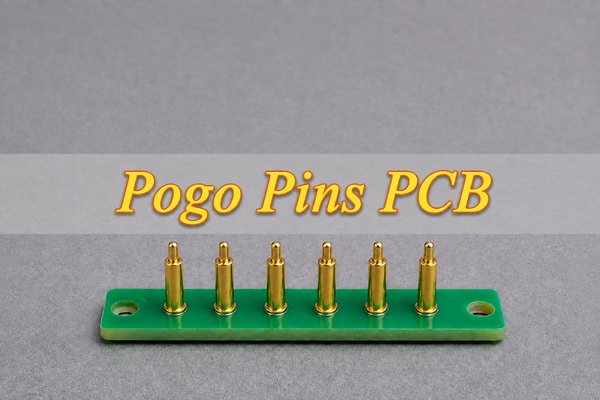
A pogo pins PCB assembly can pass a bench continuity check and still disconnect when the enclosure closes or the board bends. The spring-loaded contacts need enough compression to maintain contact, a landing surface that tolerates misalignment, and a board that carries the load without moving out of position. These requirements affect the PCB layout and assembly method before the first prototype is ordered.
EBest Circuit (Best Technology) supports PCB design, fabrication, component sourcing and assembly for prototype and production orders. For a custom pogo-pin carrier, the starting information is the contact part number, mating geometry and electrical load. A sample build can then answer specific questions about fit, contact stability and manufacturability before you commit to production.
Which Applications Need a Custom Pogo Pin PCB Assembly?
Pogo-pin carriers suit connections that must separate repeatedly or reach exposed pads without a permanently attached plug. The application determines what to design around:
- Charging docks: Check the current through both the supply and return contacts, then the force needed to keep the device seated. If charging stops when the device rocks, adding a higher-current pin will not correct the mechanical movement. Guide features and retention belong in the prototype alongside the PCB.
- Removable modules: Locate the module before its pads touch the plungers. A tapered guide or keyed housing can limit sideways entry; the pins should compress along their intended axis. Mark orientation and power/signal assignments on both drawings so a reversed module cannot silently swap connections.
- Programming fixtures: Match each probe to an accessible target pad and a defined net. Check tall components, board-location holes and tool access in the same view. For frequently serviced fixtures, a replaceable probe-and-receptacle arrangement may be more practical than soldering every probe directly into the carrier.
- Functional test fixtures: Separate the force applied by the probe array from the force used to locate the board. Support the unit under test near the loaded area and identify power, return and measurement connections. A carrier PCBA is one part of the fixture; probe plates, wiring, controls and test software must also be accounted for.
How Do You Choose SMT, Soldered Through-Hole or Press-Fit Mounting?
Choose SMT for a surface-soldered contact, through-hole soldering for a solder-tail contact, or a press-fit carrier with a separately specified electrical termination. The useful comparison is how each complete mounting arrangement connects to your circuit and fits your assembly process.
| Mounting Option | Electrical Connection | Selection Trade-off |
|---|---|---|
| SMT solder mount | The contact base is soldered to a PCB surface pad. | Suits a reflow assembly process when the part supports automated pickup. Check pad geometry, seating stability and reflow limits; a tall contact may need a pickup cap or positioning support. |
| Through-hole solder mount | A solder tail passes through the board and is soldered to the specified plated hole or land. | Suits a contact supplied with a PCB solder tail. Allow tail clearance and soldering access; match the finished hole and board thickness to the drawing. The hole alone does not prevent tilt. |
| Press-fit carrier with wire termination | The body is retained in a specified hole or housing; a solder cup or attached wire carries the electrical connection. | Useful when the contacts must sit in a housing away from the circuit board. Adds wire routing and termination work; control the receiving-hole fit and insertion depth. Do not treat the retaining hole as an electrical joint. |
“Press-fit” describes retention unless the manufacturer also specifies an electrical press-fit connection. The Mill-Max 0947, for example, is retained in a non-plated hole or insulator and connects through a solder cup. Its mounting hole does not provide a plated-through-hole electrical path.
A locating peg does not, by itself, identify the soldering method. Some Harwin SMT pogo pins have longer pegs that the manufacturer also permits for throughboard termination. Use the exact part drawing to decide which pad, hole and solder joint to specify.
For a board populated mainly by reflow, first check a compatible SMT part. If the selected contact requires a solder tail, plan the insertion and soldering operation. If the enclosure must hold the contacts separately, evaluate a wired carrier. Current rating, working travel and mating life must still be checked for the selected part; none can be ranked reliably from the mounting label alone.
How Much Compression and Working Travel Does the Assembly Need?
Every pin must remain within its recommended working range at the smallest and largest assembled gaps. Free height describes the unloaded contact; working height describes it under compression. Harwin’s P70-1010045R, for example, has a 5 mm free height and a 4 mm working height. The recommended operating point must not be confused with the absolute end of travel.
Use one mechanical datum for both dimensions: H is the assembled free tip height above that datum, and G is the distance to the mating contact surface. Compression is C = H − G. Include mounting offsets, target thickness and relevant tolerances; do not subtract dimensions taken from different board surfaces.
Worked example, using hypothetical design inputs: H = 5.00 ± 0.10 mm, G = 4.10 ± 0.15 mm, and an allowed compression range of 0.60–1.20 mm. These are illustrative assumptions, not the tolerances or working limits of the Harwin part.
- Least compression: The shortest installed pin meets the largest gap: 4.90 − 4.25 = 0.65 mm. The margin above the assumed 0.60 mm minimum is only 0.05 mm.
- Greatest compression: The tallest installed pin meets the smallest gap: 5.10 − 3.95 = 1.15 mm. Only 0.05 mm remains below the assumed 1.20 mm maximum.
- Board deflection: If loading increases the gap by a further 0.08 mm, minimum compression falls to 0.57 mm. That misses the assumed minimum by 0.03 mm, even though the nominal assembly looked acceptable.
For these inputs, the total worst-case variation in H and G consumes 0.50 mm of the 0.60 mm working window. Only 0.10 mm remains across both ends. Simply moving the nominal gap cannot recover more than that total margin: supporting the board or reducing dimensional variation addresses the missing clearance more directly. Check the assembled gap at both extremes, then verify the proposed change with the actual parts.
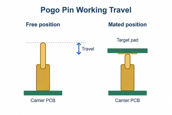
The enclosure should have a mechanical stop before the contact reaches its travel limit. Also add the spring forces at the chosen working position. As a separate illustrative estimate, eight contacts at 0.6 N each oppose closure with 4.8 N before other loads are included. Use the selected part’s force-versus-travel tolerances to size retention and check board bending; magnet pull measured under different gap conditions is not a substitute.
How Should Pogo Pin Mating Pads Be Sized and Finished?
The mating pad must contain the possible contact positions without letting the tip land on solder mask, a via opening or neighboring copper. Size that landing area separately from the solder land used to attach the pin.
For a circular landing area, a conservative geometric starting point is Dpad ≥ Dtip + 2(E + M). Here Dtip is the maximum projected tip diameter, E is the maximum radial position error, and M is the extra edge allowance. Any wipe motion must already be included in E. This checks geometric containment; it does not establish contact pressure, wear life or electrical clearance.
Illustrative pad calculation: Assume a 1.00 mm tip diameter, radial position error of 0.25 mm, and 0.10 mm edge allowance. The calculated minimum diameter is 1.70 mm. At an assumed 2.00 mm pad pitch, only 0.30 mm of copper-to-copper gap remains. Check whether that gap meets the circuit’s clearance needs and whether solder mask can be manufactured as intended before adopting the dimensions.
- Position error: Include enclosure play, board location, contact placement and target-pad registration. If the drawing gives independent X and Y limits, evaluate their combined radial error; ±0.25 mm on both axes is not a 0.25 mm radial limit.
- Wear surface: Choose the finish with the expected engagement count and motion in mind. For frequent mating, discuss a wear-rated finish or a separate target contact, and test the proposed pair. A solderability finish alone does not demonstrate acceptable resistance after repeated engagement.
- Flatness and keepouts: Keep exposed holes, silkscreen and coating away from the swept contact area. When routing requires a via there, define filling, capping and surface flatness with the fabricator rather than accepting an open depression under the tip.
A separate target introduces its own dimensions. Harwin’s S70-332002045R contact pad is a 3.2 mm diameter, 0.2 mm thick gold-finished mating component. It is an example, not the recommended pad for every design. Its installed height, including the solder joint where relevant, changes G in the compression calculation.
How Do You Check Current Capacity, Voltage Drop and Heating?
Start with the allowable voltage loss at the load, then check both the contact rating and the resistance of the complete supply-and-return path. Include the pin, mating interface, solder joints, traces and vias. A catalog rating for one contact does not automatically apply to a closely spaced array inside an enclosure.
Voltage drop is V = I × R; resistive heating is P = I² × R. Suppose each of two mated contacts, one supply and one return, contributes an assumed 0.05 Ω. At 2 A, their combined 0.10 Ω causes 0.20 V of drop and 0.40 W of heating, before PCB and wiring losses. Counting only the supply contact would miss half of this contact contribution.
If the hypothetical product permits only 0.15 V of total connection loss at 2 A, the complete path budget is 0.075 Ω. The two assumed contacts already exceed it. Reducing trace resistance alone cannot fix that selection; investigate a lower-resistance contact arrangement and verify it under the intended compression and load. None of these assumed values establishes a safe temperature or current rating.
- Load all intended power contacts together: Measure drop and temperature with the enclosure fitted and the contacts at the specified working position. Record ambient temperature and wait for the defined stabilization condition; a brief open-bench reading can miss the final temperature rise.
- Check parallel paths: Two pins do not necessarily share current equally. Contact variation and unequal routing can concentrate the load in one path. Check the individual branches and decide what the circuit must do if one contact becomes resistive or opens.
- Assess signal behavior separately: For fast edges, account for the contact geometry, PCB transitions and return path. Check the complete channel with an appropriate model or measurement; a DC continuity or current test does not demonstrate signal integrity.
What Prevents Tilt, Sticking and Damage During Assembly?
Control the fixed barrel’s position during joining, then check installed height and plunger movement after the process. Electrical continuity will not reveal every assembly defect.
- Check the exact incoming part: Compare the manufacturer part number, termination, free height and packaging with the BOM and drawing. Hold any substitute for review if its dimensions or force curve differ; matching pitch is not enough.
- Establish a repeatable seating position: Use the specified locating feature or fixture and measure from the drawing datum. Check barrel tilt before joining, when correction does not require solder rework. A contact that leans slightly can shift its tip beyond the pad allowance at full height.
- Use the part-specific joining process: For SMT, check upright stability, solder distribution and reflow limits. For solder tails, provide access and barrel support. For press-fit retention, support the receiving part and control insertion depth using the approved tooling. Inspect seating and the electrical termination as separate features where necessary.
- Measure and exercise the assembled contacts: Check tip heights with suitable metrology or a defined gauge. Compress each plunger within its working range and observe return. Investigate a slow or sticking pin for contamination, damage or process exposure; repeated pressing is not a repair.
- Protect the contact array in transit: Keep tray lids and neighboring boards away from the plungers. Check a packed sample for side loading, unintended compression and loose movement so a good assembly is not damaged after inspection.
Compare the first articles with the planned production method. Hand-positioned prototypes do not demonstrate that a tall contact will remain upright through automated placement and reflow. Resolve that difference before using prototype yield to estimate production cost.
How Should Prototypes and Pilot Builds Be Tested?
Test prototypes with the actual mating parts, then use a pilot build to check assembly consistency. Set limits from the device requirements and selected contact specifications before testing; “continuity passed” is too vague to accept a charging or frequently mated interface.
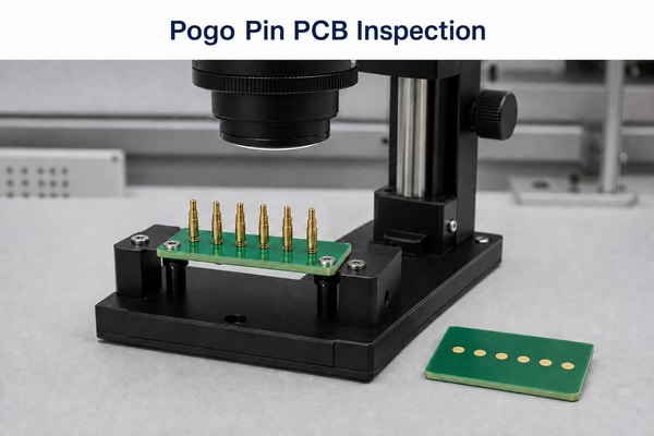
- Check fit at the tolerance extremes: Assemble the actual locating and retention hardware. Use measured parts or a controlled fixture to reproduce minimum and maximum gap and lateral offset. Record whether every tip stays on its pad and within working travel, without relying on hand pressure.
- Measure the intended resistance: Use four-wire sensing for low-resistance checks, with sense connections close to the two ends of the path being measured. Mark those points on the test drawing; measurements that include different trace lengths are not directly comparable. Record test current, compression and whether the result includes one contact or the complete loop. Use the component’s specified low-level test conditions when checking signal-contact resistance.
- Test under operating load: Load the supply and return paths together and measure voltage at the receiving circuit. Log contact-area temperature and ambient conditions until the agreed stabilization point. Compare with the voltage-loss and temperature limits, including worst-case enclosure conditions.
- Look for intermittent connections: Reproduce the allowed rocking or movement while monitoring continuity or powered function with time resolution appropriate to the system. A slowly updating handheld meter may miss a brief interruption. Record interruption duration or the resulting reset, communication error or charging fault.
- Repeat after the required use cycle: Define engagement count, speed, stroke and relevant contamination or environmental exposure. Compare resistance, loaded performance, tip return and surface wear before and after the test. Keep the mating pad finish and hardware unchanged so a contact-only catalog life claim is not mistaken for a qualified assembly.
- Compare the pilot units: Record installed-height spread, tilt, solder or insertion defects, and loaded mating results across the agreed sample. Set production inspection and sampling from the demonstrated process and risk. Identify whether an outlier follows a component lot, fixture position or assembly operation before increasing volume.
If a pogo pins PCB works only when pushed down by hand, check the gap, retention and board deflection first. If failures appear only after cycling, inspect wear and contamination and repeat the same resistance measurement. The test must reproduce the failure condition before it can tell you which change helped.
What Information Is Needed for a Custom Assembly Quote?
Send the board files and the mating requirements together. Otherwise, two suppliers may quote different assemblies even when their board quantities match.
- PCB files: Supply Gerber or ODB++, drill data, outline, stackup and finish requirements. Include the schematic or net data for electrical review and testing. If design work is still needed, identify the missing files and provide the interface requirements.
- BOM and sourcing: List manufacturer part numbers, quantities per board and approved alternatives. Attach the contact drawing and installation guidance. State which components you will supply and which EBest should source; replacements that change height or force require renewed mechanical checks.
- Mating geometry: Provide contact coordinates, datum references, operating gap and tolerances, target-pad dimensions and retention details. Include a STEP model or mating drawing and identify whether the quote includes the carrier only, a mating board, or both.
- Test requirements: State current per contact, simultaneous loads, voltage-loss limits, engagement requirements and relevant environmental conditions. Name the measurements, limits, sample plan and report expected. For programming, include the image, interface and verification method; identify who supplies the fixture and mating hardware.
- Order plan: Give prototype quantity, production quantities, required delivery date, traceability and packing needs. Identify the design or sample approvals that must happen before the production order can proceed.
Ask for separate prices for one-time tooling or test setup and recurring assembly. A higher unit quote may include component procurement, a mating board or inspection that another quote omits. Compare the same BOM, quantities, supplied items and acceptance requirements before choosing on price.
Contact availability, PCB fabrication, fixture preparation and sample approval all affect the schedule. Confirm which items are on the critical path and which delivery dates depend on your files or hardware. Send the available documents to sales@bestpcbs.com for a free DFM review and a quotation identifying the remaining inputs.
Why Choose EBest Circuit for Custom Pogo Pin PCB Assembly?
EBest combines PCB design, fabrication, component sourcing and assembly services, allowing you to purchase the carrier as a populated board. These services can support the following stages of your project:
- Before the first build: Use PCB design support and a free DFM review to resolve footprint, hole and board-manufacturing questions. Supply the contact drawing and mating dimensions; a PCB manufacturability review does not replace mechanical qualification of the enclosure.
- During prototyping: Order the carrier and any agreed mating board for evaluation with your hardware. Use the measured fit and electrical results to decide whether to revise pad size, support, contact selection or assembly requirements before a larger build.
- For component procurement: Have sourcing follow the selected BOM, with alternatives identified for approval. Keeping the contact part number controlled helps prevent a purchasing substitution from changing compression or installation requirements.
- When moving to production: Order against the accepted board revision, BOM and agreed inspection plan. Confirm the included boards, populated components, tooling and reports in the quotation. Complete fixture development and specialist reliability testing require separate confirmation.
FAQs About Pogo Pin PCB Assemblies
Q1: Is a six-pin pogo interface a standard pinout?
A1: No. Six is only the contact count. Define power, return and signal assignments, the viewing direction and a clear pin-one reference on both mating drawings. Check the reversed orientation as well as the intended one before approving the layout.
Q2: Should exposed charging contacts remain energized?
A2: That depends on the product’s protection design. Evaluate shorts from metal objects, incorrect mating and the connection sequence. Where needed, use current limiting or controlled power enable and test those functions with the actual dock; selecting a pogo pin does not provide this protection.
Q3: How should conformal-coating keepouts be specified?
A3: Mark the landing surfaces and moving-contact areas that must remain uncoated, including their location tolerances. Specify masking and inspect after coating. Protection applied over the contact surface can prevent conduction, while material entering the barrel can interfere with movement.
Q4: Can the completed carrier be washed?
A4: Only with a process permitted for the selected contact and other components. Confirm the chemistry, ingress restrictions and drying conditions before washing. Check plunger return and electrical behavior afterward; an externally clean board can still contain residue inside a moving contact.
Q5: Can a pogo pin be replaced by another part with the same pitch?
A5: Pitch alone is insufficient. Compare free and working heights, force curve, tip shape, mounting dimensions, electrical limits and process compatibility. Recalculate the gap and landing area where any of these differ, and approve the substitute before assembly.
Q6: Should a test fixture use replaceable probes?
A6: Replaceable probes can reduce maintenance rework in frequently used fixtures. Select a compatible probe and receptacle, provide removal access and identify the permitted replacement part. Verify seating and electrical performance after replacement rather than assuming any probe of the same diameter will work.
Q7: Does magnetic retention make the connection waterproof?
A7: No. Magnets provide retention, while seals and enclosure geometry control ingress. Check holding force at the real gap and evaluate sealing separately under the product’s required conditions. A magnet or gold-plated contact alone does not establish an ingress rating.
Start Your Custom Pogo Pin PCB Assembly Project
Send your PCB files, BOM with contact part numbers, mating drawing, quantities and test requirements to sales@bestpcbs.com. EBest Circuit can review the PCB manufacturing requirements and quote the agreed design, board supply, sourcing and assembly work. Include your required delivery date and the outstanding prototype checks so the next build answers the questions that still affect production.