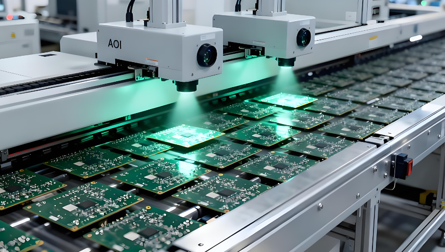
AOI inspection plays a critical role in modern PCB assembly by enabling fast, non-contact detection of surface defects before products reach functional testing or final delivery. For high-reliability industries such as automotive, medical, and industrial electronics, AOI is not just a quality checkpoint—it is a yield optimization tool.
In this guide, we will explain how AOI inspection works, what defects it can detect, how it compares with other inspection methods, and how to optimize it for maximum production efficiency.
What Is AOI Inspection in PCB Manufacturing?
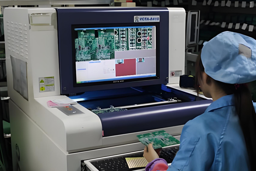
AOI inspection (Automated Optical Inspection) is a vision-based inspection method used in PCB assembly to identify defects such as missing components, solder issues, and polarity errors by comparing captured images with a reference design.
It relies on high-resolution cameras, controlled lighting systems, and image processing algorithms. The system scans each PCB and flags deviations from predefined standards. Unlike manual inspection, AOI offers high repeatability and consistent accuracy across large production volumes.
In high-mix, low-volume manufacturing environments, AOI also helps standardize quality control and reduce dependency on operator experience.
AOI Inspection in PCB Assembly
How Does AOI Inspection Work Step by Step in SMT Lines?
AOI inspection follows a structured process in SMT lines to ensure consistent defect detection across different stages of PCB assembly.
Typical AOI inspection process:
- Step 1: Image acquisition using multi-angle cameras
- Step 2: Lighting adjustment for contrast enhancement
- Step 3: Image comparison with CAD or golden board
- Step 4: Defect classification using algorithms
- Step 5: Pass/Fail decision and data logging
AOI can be placed at different stages, including post-solder paste printing, post-placement, and post-reflow, depending on inspection requirements.
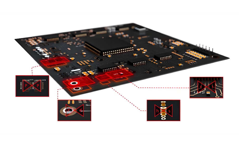
What Defects Can AOI Inspection Detect on PCB Assemblies?
AOI inspection is highly effective for detecting visible defects on PCB surfaces. It significantly reduces early-stage defects before costly downstream testing.
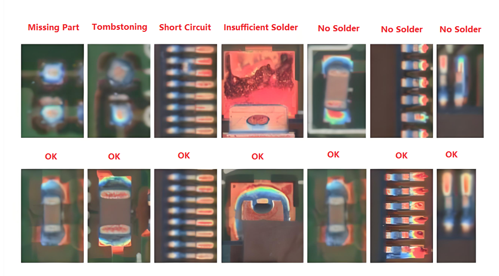
| Defect Type | Description | Detection Capability |
|---|---|---|
| Missing Component | Component not mounted | High |
| Solder Bridge | Unintended connection between pads | High |
| Misalignment | Component shifted from correct position | High |
| Tombstoning | Component standing vertically | Medium |
| Insufficient Solder | Weak or incomplete solder joint | Medium |
| Polarity Error | Incorrect component orientation | High |
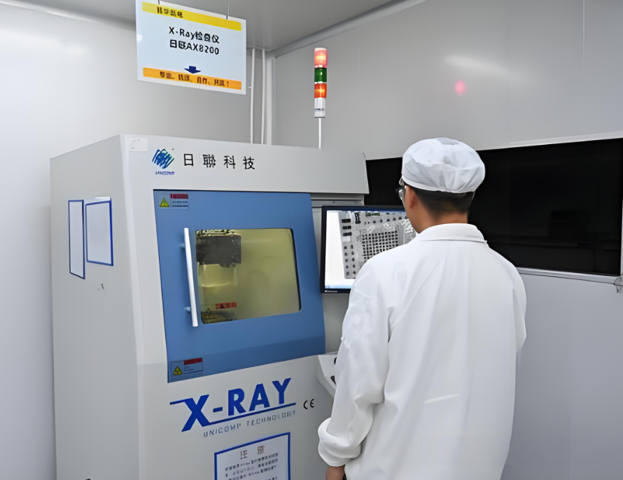
However, AOI cannot detect internal defects such as voids under BGA packages, which require X-ray inspection.
What Are the Limitations of AOI Inspection?
While AOI is highly efficient, it has inherent limitations that engineers must consider when designing inspection strategies.
- Cannot inspect hidden solder joints (BGA, QFN)
- False calls due to lighting or reflection issues
- Dependent on programming quality
- Limited ability to detect electrical defects
To overcome these limitations, AOI is often combined with X-ray inspection and ICT testing in high-reliability applications.
AOI Inspection vs X-Ray vs ICT: Which One Should You Choose?
Choosing the right inspection method depends on your product complexity, reliability requirements, and budget constraints.
| Inspection Method | Hidden Defect Detection | Speed | Cost | Best Use Case |
|---|---|---|---|---|
| AOI | No | Fast | Low | Surface defect detection |
| X-ray | Yes | Medium | High | BGA/QFN inspection |
| ICT | Electrical faults | Slow | Medium | Circuit verification |
In most SMT lines, AOI is used as the first inspection layer, followed by X-ray and ICT for critical applications.
Where Should AOI Be Placed in SMT Process for Best Results?
The placement of AOI inspection in the SMT process directly impacts defect detection efficiency and rework cost.
- Post-Printing AOI: Detect solder paste issues early
- Pre-Reflow AOI: Verify component placement
- Post-Reflow AOI: Final inspection of solder joints
For most applications, post-reflow AOI is essential, while pre-reflow AOI is recommended for high-density PCBs.
What Is the Difference Between 2D AOI and 3D AOI Systems?
2D and 3D AOI systems differ mainly in inspection depth and accuracy.
| Feature | 2D AOI | 3D AOI |
|---|---|---|
| Inspection Type | Image-based | Height & volume measurement |
| Accuracy | Moderate | High |
| Cost | Lower | Higher |
| Use Case | General SMT | High-reliability industries |
3D AOI is increasingly used in automotive and medical applications due to its ability to measure solder volume precisely.
Why Does AOI Inspection Generate False Calls and How to Reduce Them?
False calls are one of the biggest challenges in AOI inspection, often caused by lighting inconsistencies, component variations, and poor programming.
Common causes:
- Reflective surfaces
- Component color variation
- Incorrect threshold settings
- Poor reference data
Optimization methods:
- Use multi-angle lighting systems
- Optimize inspection algorithms
- Standardize component libraries
- Continuous program tuning
Reducing false calls can significantly improve production efficiency and reduce manual inspection workload.
How to Program and Optimize AOI Inspection for High Yield?
Proper AOI programming is essential to achieving high yield and minimizing defects.
- Use golden board for reference calibration
- Define clear inspection criteria based on IPC standards
- Segment inspection zones for complex PCBs
- Regularly update programs for new product variants
Experienced engineers can reduce false call rates to below 5% with optimized programming strategies.
How Much Does AOI Inspection Cost in PCB Manufacturing?
The cost of AOI inspection depends on equipment type, production volume, and inspection complexity.
| Cost Factor | Description |
|---|---|
| Equipment Investment | $50,000 – $150,000+ |
| Programming Cost | Depends on PCB complexity |
| Operational Cost | Low per unit |
Despite the initial investment, AOI significantly reduces defect-related costs and improves ROI over time.
What Standards Are Used in AOI Inspection?
AOI inspection follows international standards to ensure consistent quality and compliance.
- IPC-A-610 (Acceptability of Electronic Assemblies)
- ISO 9001 Quality Management
- IATF 16949 for automotive
- ISO 13485 for medical devices
For high-reliability applications, IPC Class 3 is commonly applied.
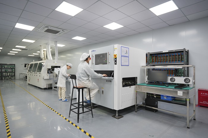
Why Choose EBest Circuit (Best Technology) for AOI Inspection Services?
With nearly 20 years of PCB and PCBA experience, EBest Circuit provides advanced AOI inspection solutions tailored for high-reliability industries.
- 3D AOI + X-ray integrated inspection capability
- IPC Class 2 & Class 3 compliance
- MES traceability system (5-second tracking)
- Experienced engineering team for AOI optimization
- Fast turnaround and stable quality
Contact us: sales@bestpcbs.com
FAQs About AOI Inspection
1. What is AOI inspection used for?
AOI inspection is used to detect surface defects in PCB assembly, ensuring product quality before functional testing.
2. Can AOI detect BGA defects?
No, AOI cannot detect hidden defects under BGA packages. X-ray inspection is required.
3. How accurate is AOI inspection?
Accuracy can exceed 95% when properly programmed and optimized.
4. Is AOI inspection expensive?
Initial investment is high, but long-term cost savings are significant.
5. What is the difference between AOI and SPI?
SPI inspects solder paste before placement, while AOI inspects components and solder joints after placement.