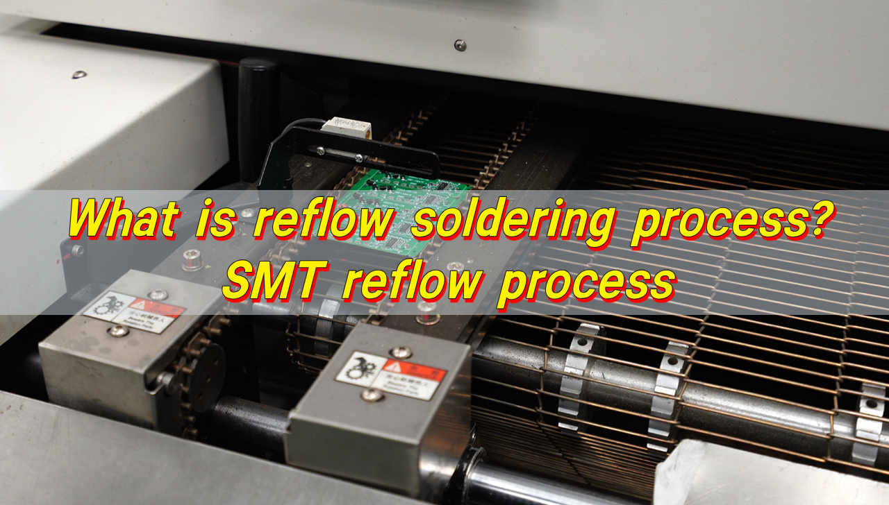
The reflow process soldering method is an SMT assembly process where solder paste is printed on PCB pads, components are placed, and the assembly passes through a controlled oven profile. The main stages are preheat, soak, reflow and cooling. Reliable results depend on paste volume, placement accuracy, peak temperature, time above liquidus, cooling rate and inspection.
The reflow soldering process is simple in principle, but reliable results depend on more than reaching the solder’s melting point. Paste volume, component placement, PCB thermal mass, oven settings, peak temperature, time above liquidus, and cooling rate all influence the final joint. A profile that works for a small two-layer PCB may therefore be unsuitable for a dense multilayer assembly with BGAs, large copper planes, or mixed component sizes.
What Is Reflow Process Soldering in Electronics Manufacturing?
Reflow process soldering is the standard method used to attach most surface-mount components to printed circuit boards. Solder paste is first printed onto PCB pads, components are placed into the paste, and the assembly then travels through a reflow oven. Controlled heating activates the flux, melts the solder alloy, forms the joints, and finally cools them into a stable connection.
Before heating, the solder paste holds the components in position. As the board enters the hotter sections of the reflow oven, the flux activates and removes oxides from the surfaces being joined. Once the solder alloy passes its liquidus temperature, it melts and wets the component terminals and PCB pads. Cooling then solidifies the solder into permanent electrical and mechanical joints.
Reflow is especially suitable for modern PCB assembly because hundreds or thousands of SMT joints can be processed during the same oven cycle. It also supports fine-pitch ICs, QFNs, BGAs, chip resistors, capacitors, and other high-density components that would be difficult to solder individually.
The process is commonly used for:
- Consumer and industrial electronics
- Automotive control boards
- Telecom and networking equipment
- Medical electronics
- Power electronics
- IoT devices
- High-density computing hardware
How Does the Reflow Soldering Process Work Step by Step?
The complete SMT reflow soldering process includes several operations before and after the PCB enters the oven. Treating the oven itself as the entire process overlooks many of the variables that determine solder-joint quality. A PCB reflow soldering process must therefore control printing, placement, heating, cooling, and inspection as one connected workflow.
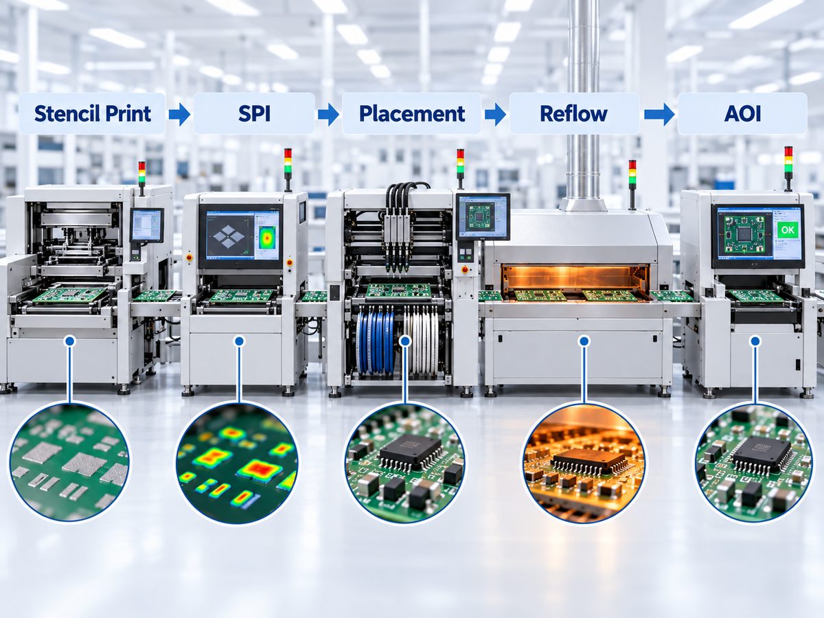
1. PCB and stencil preparation
The PCB surface and stencil must be clean and compatible with the selected solder paste. Stencil thickness and aperture design determine how much paste is transferred onto each pad.
Fine-pitch packages normally need tighter control of aperture geometry than larger passive components.
2. Solder paste printing
A stencil printer pushes solder paste through the stencil apertures and deposits it onto exposed PCB pads.
Paste height, area, volume, alignment, and release consistency matter. Too much paste can encourage bridging or solder balls, while insufficient deposits can cause weak or open joints.
3. Solder Paste Inspection
SPI equipment checks the printed deposits before components are placed. This step can identify:
- Insufficient paste
- Excess paste
- Offset deposits
- Poor stencil release
- Inconsistent paste volume
Finding these problems before placement and reflow is generally more efficient than diagnosing solder defects afterward.
4. Component placement
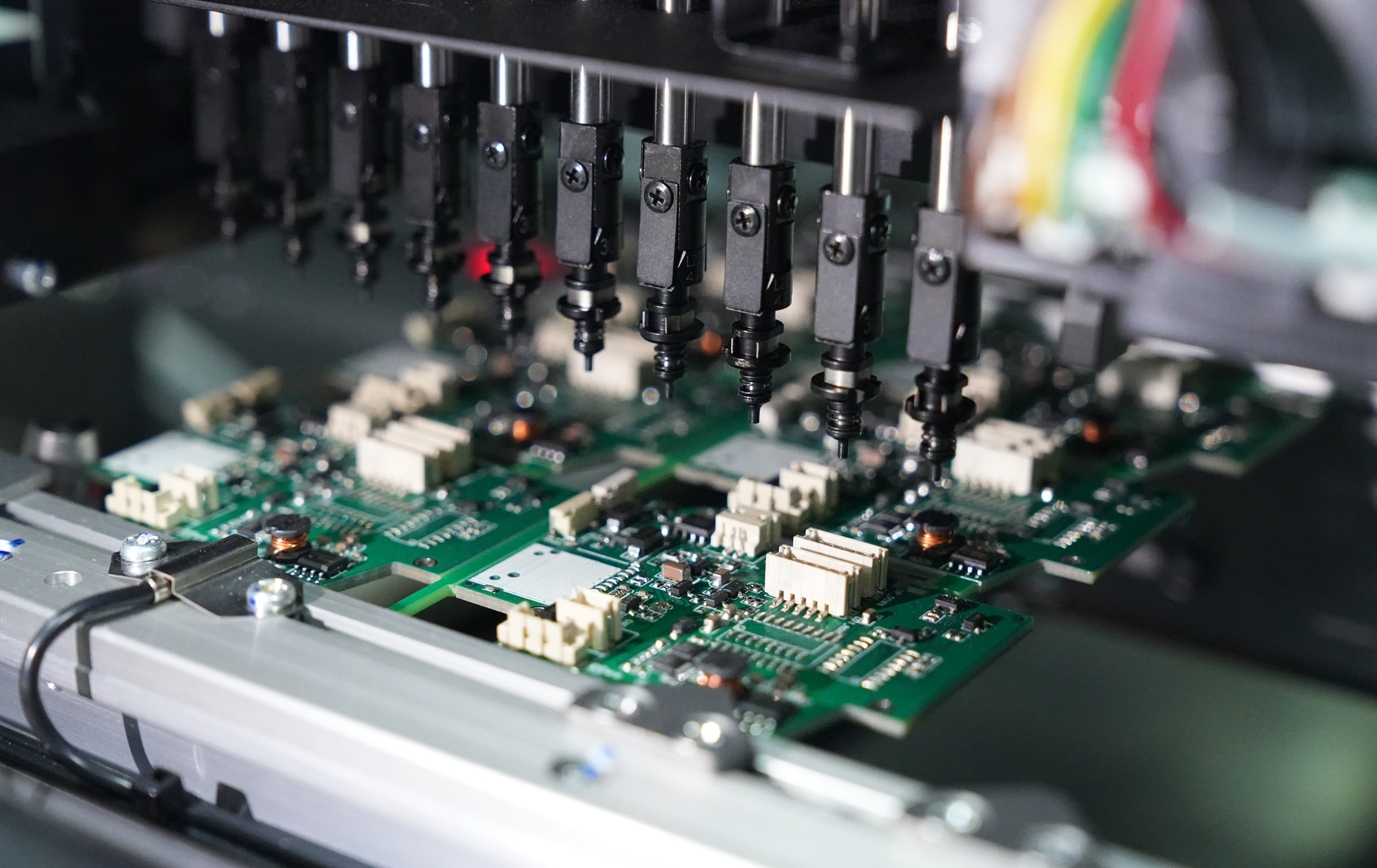
Pick-and-place equipment positions SMT components onto the printed solder paste. Placement accuracy becomes particularly important for fine-pitch ICs, small chip components, BGAs, QFNs, and boards with high component density.
Surface tension during reflow can correct small placement offsets, but it cannot compensate for large errors, incorrect polarity, severe rotation, or inappropriate pad and paste geometry.
5. Reflow soldering
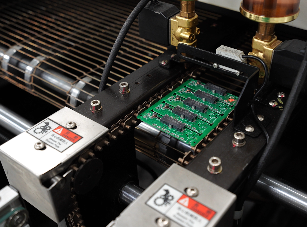
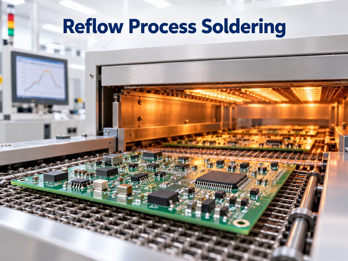
The populated PCB travels through the reflow oven on a conveyor. Multiple heating zones create a controlled temperature profile that gradually heats the assembly, activates the flux, melts the alloy, and then cools the joints.
6. Post-reflow inspection
After cooling, AOI can detect visible defects such as bridging, component shift, polarity errors, and missing components. For BGAs, QFNs, and other packages with hidden joints, X-ray inspection may be required.
What Happens During the Four Reflow Oven Stages?
The reflow oven soldering process is typically divided into preheat, soak, reflow, and cooling. Each stage has a different thermal function.
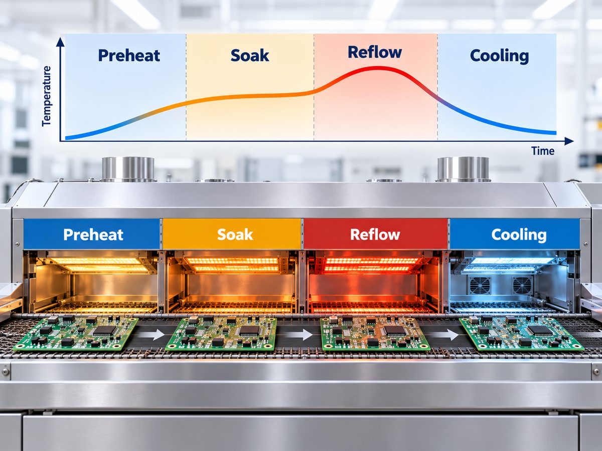
| Reflow Stage | Main Purpose | Main Control Point |
| Preheat | Raise PCB temperature gradually | Ramp rate |
| Soak | Reduce thermal differences and activate flux | Time and temperature |
| Reflow | Melt solder and form the joint | Peak temperature and TAL |
| Cooling | Solidify the solder joint | Cooling rate |
Preheat
During preheating, the PCB temperature rises gradually from ambient temperature. Excessively rapid heating can increase thermal stress, solder spattering, component damage, and temperature differences across the assembly.
For many solder paste systems, an average heating rate around 0.5–2.5°C/s can serve as a practical starting window, although the paste manufacturer’s recommended profile should take priority.
Soak
The soak stage allows different areas of the PCB to approach a more uniform temperature while the flux continues to activate.
This becomes useful on boards containing both high-thermal-mass and low-thermal-mass areas. Large copper planes, connectors, shields, BGAs, and power devices can heat more slowly than small passive components.
The exact soak range is paste-dependent rather than universal.
Reflow
During this stage, the solder passes its liquidus temperature and wets the PCB pads and component terminations.
Two parameters are especially important:
- Peak temperature
- Time Above Liquidus (TAL)
Too little thermal energy may result in incomplete wetting. Excessive temperature or excessive TAL can stress components, accelerate intermetallic growth, and degrade flux performance.
Cooling
Once the solder joint has formed, the PCB moves through the cooling zones. Controlled cooling solidifies the alloy and establishes its final microstructure.
Very slow cooling can affect joint structure, while excessively fast cooling may introduce thermal stress. The acceptable range should therefore be treated as part of the verified reflow profile rather than an isolated oven setting.
What Is Reflow Solder Paste Made Of?
Reflow solder paste is a printable mixture of metal alloy powder and flux chemistry. It must remain stable enough for stencil printing, hold components during placement, and then perform correctly as temperature rises.
Typical solder paste contains:
- Solder alloy powder: Forms the final metallic joint.
- Flux: Removes surface oxides and assists wetting.
- Activators: Improve the flux’s ability to clean solderable surfaces.
- Solvents: Help control paste consistency and processing behavior.
- Rheology modifiers: Control viscosity, slump, printing, and stencil release.
SAC305 is a widely used lead-free alloy containing approximately 96.5% tin, 3.0% silver, and 0.5% copper. Its liquidus temperature is around 217°C.
Sn63/Pb37, still used in some permitted legacy and high-reliability applications, is a eutectic alloy containing 63% tin and 37% lead with a melting point of 183°C.
Alloy selection alone is not enough. Powder size, flux classification, storage condition, stencil design, PCB finish, component termination, cleaning requirements, and process atmosphere can also affect printing and reflow performance.
What Temperature Profile Is Used for Reflow Soldering?
There is no single reflow soldering temperature profile that works for every PCB.
For lead-free SAC305 assemblies, peak temperature often falls in roughly the 230–260°C range, while the alloy liquidus is about 217°C. The exact profile must still follow the solder paste specification and the thermal behavior of the actual assembly.
A practical starting reference may look like this:
| Parameter | Typical SAC305 Starting Window |
| Average ramp rate | About 0.5–2.5°C/s |
| Soak | Paste-dependent; commonly around 140–170°C |
| Liquidus | About 217°C |
| Time Above Liquidus | About 30–100 s |
| Peak temperature | About 230–260°C |
| Cooling rate | Controlled according to paste and assembly requirements |
For Sn63/Pb37, the thermal requirement is lower. The alloy melts at 183°C, with common peak reflow temperatures around 205–215°C for applicable solder systems.
These figures are useful starting points, not fixed production settings.
The final oven recipe should account for:
- Solder paste manufacturer’s TDS
- PCB thickness and layer count
- Copper distribution
- Component density
- Large thermal-mass components
- BGA and QFN packages
- Temperature-sensitive components
- Conveyor speed
- Oven zone configuration
- Air or nitrogen atmosphere
A thermocouple profiling run is therefore more reliable than setting the oven solely from a generic temperature chart. Thermocouples should be placed at representative hot and cold locations so the engineer can confirm that all critical joints remain inside the acceptable process window.
Two profile shapes are commonly encountered: Ramp-Soak-Spike (RSS) and Ramp-to-Spike (RTS). Neither is automatically better. Paste chemistry, board construction, voiding behavior, thermal gradients, and component mix determine which approach is more appropriate.
What Equipment Is Used in the Reflow Soldering Process?
Industrial reflow soldering is part of a complete SMT production line rather than a standalone oven operation.
Typical equipment includes:
- Stencil printer
- Solder paste inspection system
- Pick-and-place machine
- Multi-zone reflow oven
- Thermal profiler and thermocouples
- AOI system
- X-ray inspection equipment when required
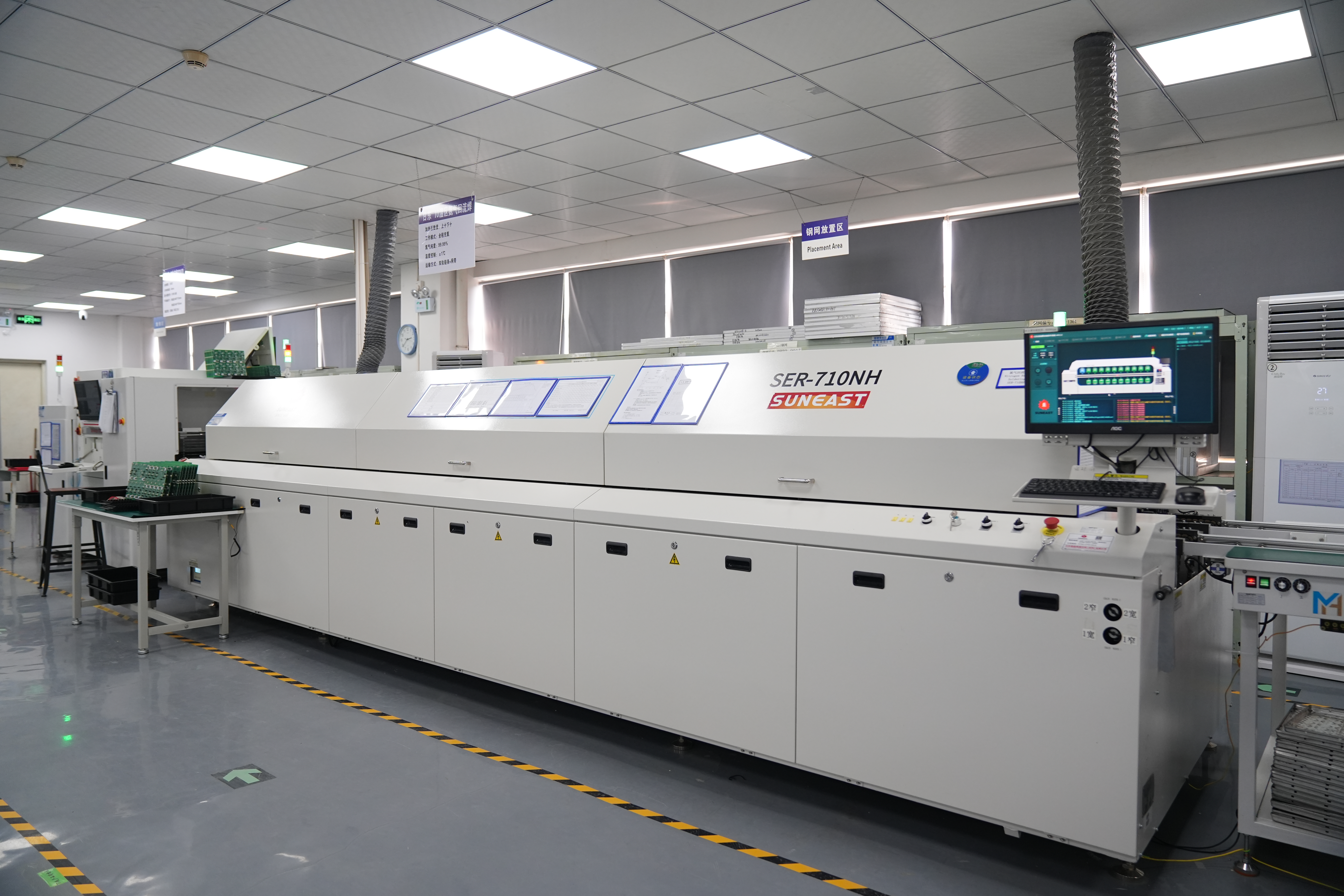
The multi-zone convection reflow oven is the central thermal-processing machine. Independent heating zones allow the line engineer to shape the PCB’s actual temperature curve rather than simply selecting one oven temperature.
Conveyor speed is equally important. A change in belt speed changes how long the PCB remains in each thermal region, which can alter soak duration, TAL, and peak temperature even when individual oven-zone setpoints remain unchanged.
Nitrogen reflow may be used when reduced oxidation or improved wetting is valuable. Vacuum reflow is used in more specialized applications where controlling solder voiding is particularly important. These processes add capability but are not mandatory for every PCBA.
What Are the Most Common Reflow Soldering Defects?
Reflow defects usually come from an interaction between printing, PCB design, component placement, material condition, and the thermal profile. Changing oven temperature alone will not solve every problem.
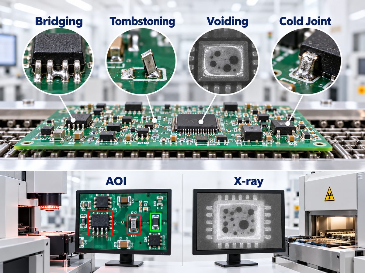
| Defect | Common Process Causes | Typical Corrective Direction |
| Tombstoning | Uneven heating, unequal paste deposits, pad imbalance | Improve thermal balance and paste consistency |
| Solder bridging | Excess paste, poor stencil design, placement offset | Adjust aperture, paste volume and placement |
| Cold or poor joints | Insufficient heat or TAL, poor wetting | Verify profile and solderability |
| Voiding | Flux outgassing, pad design, paste/profile interaction | Optimize paste, aperture and profile |
| Solder balls | Paste slump, rapid heating, contamination | Review printing, paste handling and ramp rate |
| Head-in-pillow | BGA warpage, oxidation, insufficient wetting | Review component warpage and profile |
| Component shift | Placement error or uneven wetting forces | Check placement, pads and paste distribution |
Tombstoning is a good example of why root-cause analysis matters. If one termination of a small passive component melts and wets earlier than the other, the resulting unbalanced surface tension can lift the component onto one end.
For BGA and QFN assemblies, visual inspection cannot evaluate hidden solder joints. X-ray inspection can reveal voiding, bridging, missing balls, alignment issues, and other defects underneath the package.
Reflow Soldering vs Wave Soldering: What Is the Difference?
Reflow soldering is primarily associated with SMT components, while wave soldering is mainly used for through-hole components. The two processes also deliver solder in fundamentally different ways.
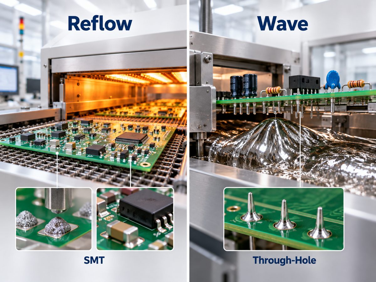
| Factor | Reflow Soldering | Wave Soldering |
| Main component type | SMT | Through-hole |
| Solder source | Printed solder paste | Molten solder bath |
| Heating method | Controlled reflow oven | PCB passes over solder wave |
| Fine-pitch SMT | Well suited | Generally unsuitable |
| Typical production use | SMT assembly | THT assembly |
| Joint formation | Paste melts on individual pads | Exposed joints contact molten solder |
Mixed-technology PCBAs may use both processes. SMT components can be reflowed first, followed by wave or selective soldering for through-hole components that cannot be processed during the SMT reflow stage.
The correct choice therefore depends less on which process is “better” and more on the component technology, PCB layout, heat sensitivity, production volume, and assembly sequence.
FAQs About Reflow Process Soldering
1. Which is the second stage in the reflow soldering process?
If the question refers to the four thermal stages inside a reflow oven, the second stage is the soak stage, following preheat. In a complete SMT manufacturing workflow, however, manufacturers may divide and number printing, SPI, placement, reflow, and inspection differently.
2. What temperature is used for reflow soldering?
For SAC305 lead-free solder, peak temperatures commonly fall within roughly 230–260°C, depending on the solder paste and assembly. Sn63/Pb37 uses a lower thermal profile and may peak around 205–215°C. The solder paste TDS and measured board profile should take priority over a generic peak-temperature value.
3. What is Time Above Liquidus in reflow soldering?
Time Above Liquidus, or TAL, is the period during which the solder joint remains hotter than the alloy’s liquidus temperature. It must be long enough to achieve suitable melting and wetting without subjecting the assembly to unnecessary thermal exposure.
For SAC305 processes, a range around 30–100 seconds may be encountered depending on the solder paste, although the correct value remains paste- and assembly-specific.
4. What solder paste is used for reflow soldering?
Lead-free SAC305 is widely used in current electronics assembly. Other alloys are selected for lower temperature, reliability, cost, regulatory, or application-specific requirements. The flux system and powder size must also match the PCB, stencil, component pitch, storage conditions, and cleaning process.
5. Can through-hole components be reflow soldered?
Some through-hole components can be assembled using pin-in-paste or intrusive reflow, where solder paste is printed around or into plated through-holes before the component is inserted and reflowed.
The component must tolerate the thermal profile, and sufficient solder volume must be provided to achieve acceptable barrel fill. For many conventional through-hole assemblies, wave or selective soldering remains more practical.
6. What is the difference between wave soldering and reflow soldering?
Reflow soldering heats deposited solder paste and is mainly used for SMT assembly. Wave soldering moves the underside of the PCB across a controlled wave of molten solder and is mainly used for through-hole assembly. Mixed PCBAs may use reflow for SMT first and wave or selective soldering afterward.
How Can EBest Circuit Support Your Reflow Soldering Project?
If you are preparing a PCB or PCBA project and need support with soldering process requirements, assembly manufacturability, or production planning, send your Gerber files, BOM, and assembly requirements to sales@bestpcbs.com. Our engineering team can review the project before production and help identify process conditions that may affect solder-joint quality, component reliability, or assembly yield.