PCB manufacturing PCB manufacturing
Home > Blog

reflow process soldering

Reflow Process Soldering: SMT Steps, Temperature Profile & Defects
Wednesday, September 9th, 2026

The reflow process soldering method is an SMT assembly process where solder paste is printed on PCB pads, components are placed, and the assembly passes through a controlled oven profile. The main stages are preheat, soak, reflow and cooling. Reliable results depend on paste volume, placement accuracy, peak temperature, time above liquidus, cooling rate and inspection.

The reflow soldering process is simple in principle, but reliable results depend on more than reaching the solder’s melting point. Paste volume, component placement, PCB thermal mass, oven settings, peak temperature, time above liquidus, and cooling rate all influence the final joint. A profile that works for a small two-layer PCB may therefore be unsuitable for a dense multilayer assembly with BGAs, large copper planes, or mixed component sizes.
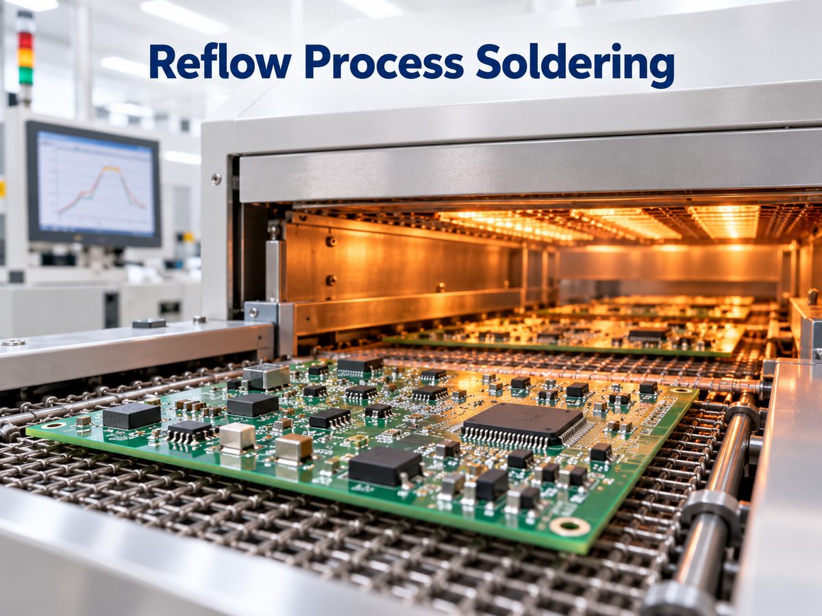
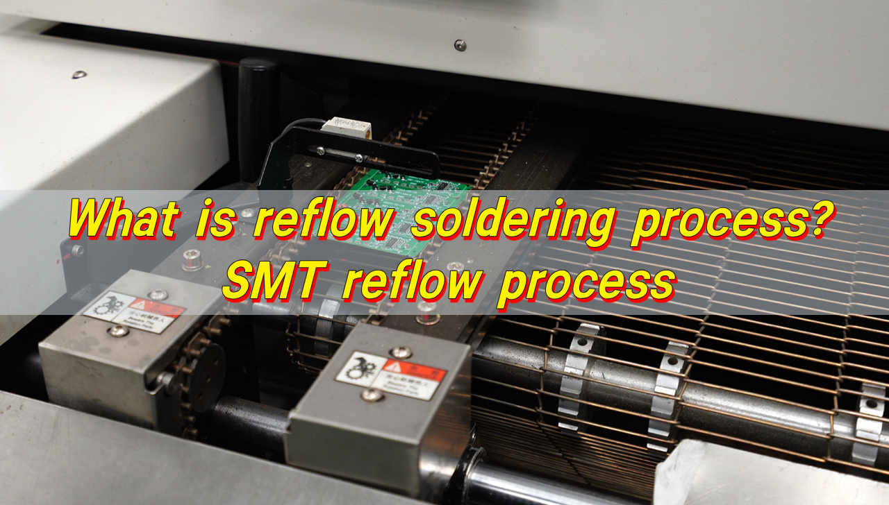
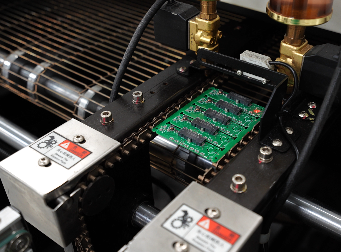
Reflow process soldering line with a populated PCB moving through a reflow oven

What Is Reflow Process Soldering in Electronics Manufacturing?

Reflow process soldering is the standard method used to attach most surface-mount components to printed circuit boards. Solder paste is first printed onto PCB pads, components are placed into the paste, and the assembly then travels through a reflow oven. Controlled heating activates the flux, melts the solder alloy, forms the joints, and finally cools them into a stable connection.

Before heating, the solder paste holds the components in position. As the board enters the hotter sections of the reflow oven, the flux activates and removes oxides from the surfaces being joined. Once the solder alloy passes its liquidus temperature, it melts and wets the component terminals and PCB pads. Cooling then solidifies the solder into permanent electrical and mechanical joints.

Reflow is especially suitable for modern PCB assembly because hundreds or thousands of SMT joints can be processed during the same oven cycle. It also supports fine-pitch ICs, QFNs, BGAs, chip resistors, capacitors, and other high-density components that would be difficult to solder individually.

The process is commonly used for:

  • Consumer and industrial electronics
  • Automotive control boards
  • Telecom and networking equipment
  • Medical electronics
  • Power electronics
  • IoT devices
  • High-density computing hardware

How Does the Reflow Soldering Process Work Step by Step?

The complete SMT reflow soldering process includes several operations before and after the PCB enters the oven. Treating the oven itself as the entire process overlooks many of the variables that determine solder-joint quality. A PCB reflow soldering process must therefore control printing, placement, heating, cooling, and inspection as one connected workflow.
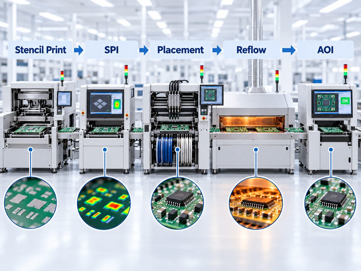
SMT reflow soldering workflow showing stencil printing, SPI, placement, reflow and AOI

1. PCB and stencil preparation

The PCB surface and stencil must be clean and compatible with the selected solder paste. Stencil thickness and aperture design determine how much paste is transferred onto each pad.

Fine-pitch packages normally need tighter control of aperture geometry than larger passive components.

2. Solder paste printing

A stencil printer pushes solder paste through the stencil apertures and deposits it onto exposed PCB pads.

Paste height, area, volume, alignment, and release consistency matter. Too much paste can encourage bridging or solder balls, while insufficient deposits can cause weak or open joints.

3. Solder Paste Inspection

SPI equipment checks the printed deposits before components are placed. This step can identify:

  • Insufficient paste
  • Excess paste
  • Offset deposits
  • Poor stencil release
  • Inconsistent paste volume

Finding these problems before placement and reflow is generally more efficient than diagnosing solder defects afterward.

4. Component placement

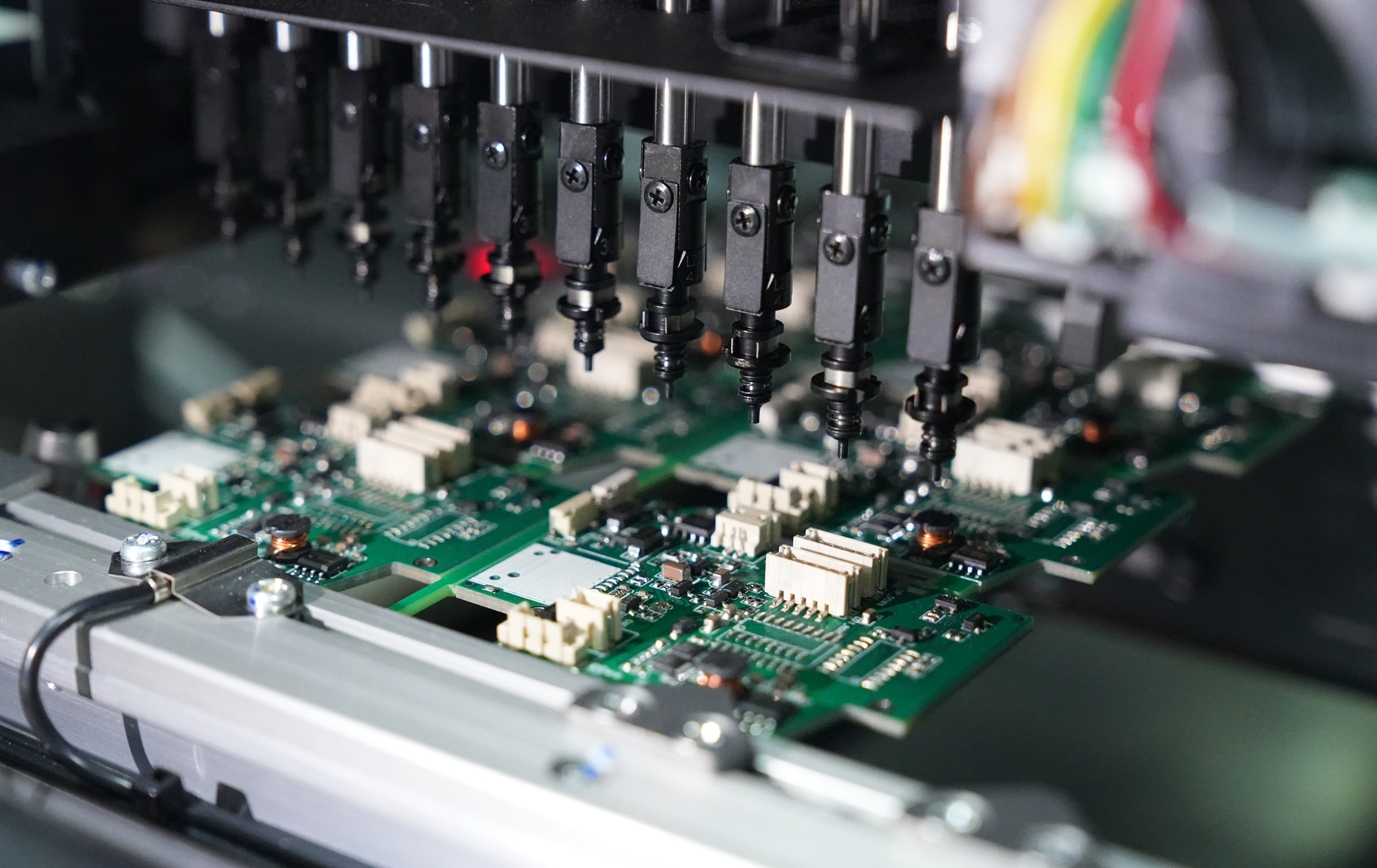
Pick-and-place equipment positions SMT components onto the printed solder paste. Placement accuracy becomes particularly important for fine-pitch ICs, small chip components, BGAs, QFNs, and boards with high component density.

Surface tension during reflow can correct small placement offsets, but it cannot compensate for large errors, incorrect polarity, severe rotation, or inappropriate pad and paste geometry.

5. Reflow soldering

The populated PCB travels through the reflow oven on a conveyor. Multiple heating zones create a controlled temperature profile that gradually heats the assembly, activates the flux, melts the alloy, and then cools the joints.

6. Post-reflow inspection

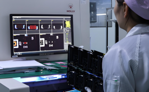
After cooling, AOI can detect visible defects such as bridging, component shift, polarity errors, and missing components. For BGAs, QFNs, and other packages with hidden joints, X-ray inspection may be required.

What Happens During the Four Reflow Oven Stages?

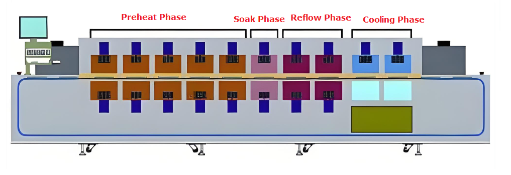
The reflow oven soldering process is typically divided into preheat, soak, reflow, and cooling. Each stage has a different thermal function.
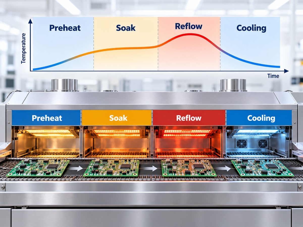
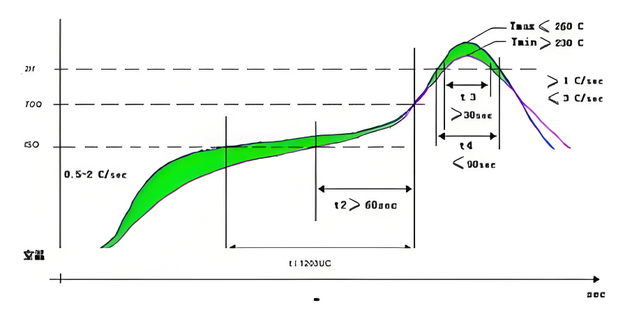
Four reflow oven stages and temperature profile: preheat, soak, reflow and cooling
Reflow Stage Main Purpose Main Control Point
Preheat Raise PCB temperature gradually Ramp rate
Soak Reduce thermal differences and activate flux Time and temperature
Reflow Melt solder and form the joint Peak temperature and TAL
Cooling Solidify the solder joint Cooling rate

Preheat

During preheating, the PCB temperature rises gradually from ambient temperature. Excessively rapid heating can increase thermal stress, solder spattering, component damage, and temperature differences across the assembly.

For many solder paste systems, an average heating rate around 0.5–2.5°C/s can serve as a practical starting window, although the paste manufacturer’s recommended profile should take priority.

Soak

The soak stage allows different areas of the PCB to approach a more uniform temperature while the flux continues to activate.

This becomes useful on boards containing both high-thermal-mass and low-thermal-mass areas. Large copper planes, connectors, shields, BGAs, and power devices can heat more slowly than small passive components.

The exact soak range is paste-dependent rather than universal.

Reflow

During this stage, the solder passes its liquidus temperature and wets the PCB pads and component terminations.

Two parameters are especially important:

  • Peak temperature
  • Time Above Liquidus (TAL)

Too little thermal energy may result in incomplete wetting. Excessive temperature or excessive TAL can stress components, accelerate intermetallic growth, and degrade flux performance.

Cooling

Once the solder joint has formed, the PCB moves through the cooling zones. Controlled cooling solidifies the alloy and establishes its final microstructure.

Very slow cooling can affect joint structure, while excessively fast cooling may introduce thermal stress. The acceptable range should therefore be treated as part of the verified reflow profile rather than an isolated oven setting.

What Is Reflow Solder Paste Made Of?

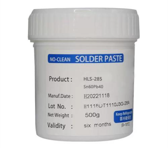
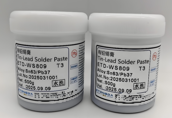
Reflow solder paste is a printable mixture of metal alloy powder and flux chemistry. It must remain stable enough for stencil printing, hold components during placement, and then perform correctly as temperature rises.

Typical solder paste contains:

  • Solder alloy powder: Forms the final metallic joint.
  • Flux: Removes surface oxides and assists wetting.
  • Activators: Improve the flux’s ability to clean solderable surfaces.
  • Solvents: Help control paste consistency and processing behavior.
  • Rheology modifiers: Control viscosity, slump, printing, and stencil release.

SAC305 is a widely used lead-free alloy containing approximately 96.5% tin, 3.0% silver, and 0.5% copper. Its liquidus temperature is around 217°C.

Sn63/Pb37, still used in some permitted legacy and high-reliability applications, is a eutectic alloy containing 63% tin and 37% lead with a melting point of 183°C.

Alloy selection alone is not enough. Powder size, flux classification, storage condition, stencil design, PCB finish, component termination, cleaning requirements, and process atmosphere can also affect printing and reflow performance.

What Temperature Profile Is Used for Reflow Soldering?

There is no single reflow soldering temperature profile that works for every PCB.

For lead-free SAC305 assemblies, peak temperature often falls in roughly the 230–260°C range, while the alloy liquidus is about 217°C. The exact profile must still follow the solder paste specification and the thermal behavior of the actual assembly.

A practical starting reference may look like this:

Parameter Typical SAC305 Starting Window
Average ramp rate About 0.5–2.5°C/s
Soak Paste-dependent; commonly around 140–170°C
Liquidus About 217°C
Time Above Liquidus About 30–100 s
Peak temperature About 230–260°C
Cooling rate Controlled according to paste and assembly requirements

For Sn63/Pb37, the thermal requirement is lower. The alloy melts at 183°C, with common peak reflow temperatures around 205–215°C for applicable solder systems.

These figures are useful starting points, not fixed production settings.

The final oven recipe should account for:

  • Solder paste manufacturer’s TDS
  • PCB thickness and layer count
  • Copper distribution
  • Component density
  • Large thermal-mass components
  • BGA and QFN packages
  • Temperature-sensitive components
  • Conveyor speed
  • Oven zone configuration
  • Air or nitrogen atmosphere

A thermocouple profiling run is therefore more reliable than setting the oven solely from a generic temperature chart. Thermocouples should be placed at representative hot and cold locations so the engineer can confirm that all critical joints remain inside the acceptable process window.

Two profile shapes are commonly encountered: Ramp-Soak-Spike (RSS) and Ramp-to-Spike (RTS). Neither is automatically better. Paste chemistry, board construction, voiding behavior, thermal gradients, and component mix determine which approach is more appropriate.

What Equipment Is Used in the Reflow Soldering Process?

Industrial reflow soldering is part of a complete SMT production line rather than a standalone oven operation.

Typical equipment includes:

  • Stencil printer
  • Solder paste inspection system
  • Pick-and-place machine
  • Multi-zone reflow oven
  • Thermal profiler and thermocouples
  • AOI system
  • X-ray inspection equipment when required

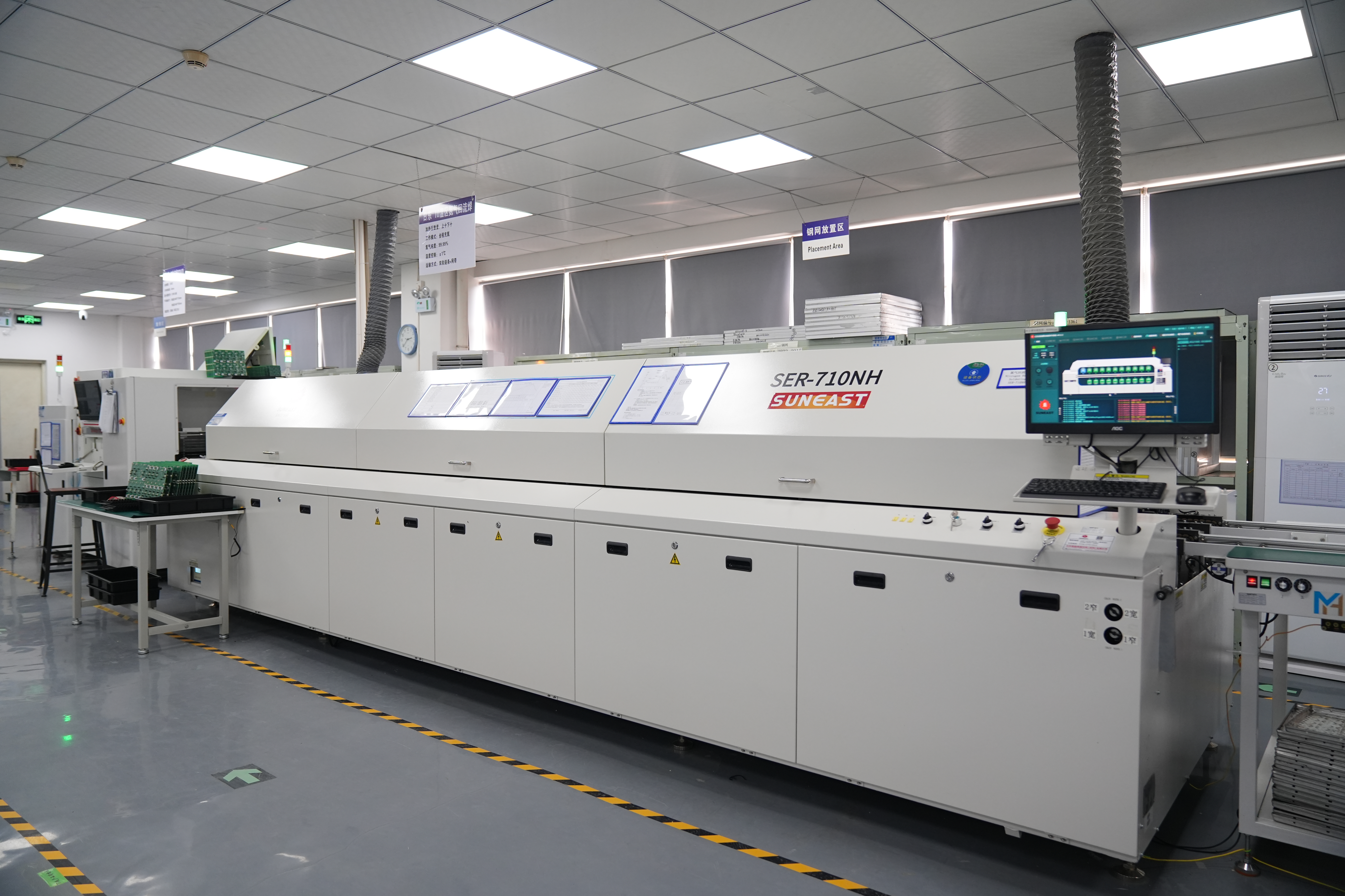
The multi-zone convection reflow oven is the central thermal-processing machine. Independent heating zones allow the line engineer to shape the PCB’s actual temperature curve rather than simply selecting one oven temperature.

Conveyor speed is equally important. A change in belt speed changes how long the PCB remains in each thermal region, which can alter soak duration, TAL, and peak temperature even when individual oven-zone setpoints remain unchanged.

Nitrogen reflow may be used when reduced oxidation or improved wetting is valuable. Vacuum reflow is used in more specialized applications where controlling solder voiding is particularly important. These processes add capability but are not mandatory for every PCBA.

What Are the Most Common Reflow Soldering Defects?

Reflow defects usually come from an interaction between printing, PCB design, component placement, material condition, and the thermal profile. Changing oven temperature alone will not solve every problem.
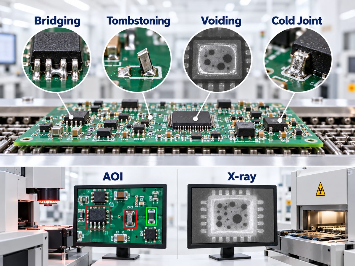
Common reflow soldering defects including bridging, tombstoning, voiding and cold joints with AOI and X-ray inspection
Defect Common Process Causes Typical Corrective Direction
Tombstoning Uneven heating, unequal paste deposits, pad imbalance Improve thermal balance and paste consistency
Solder bridging Excess paste, poor stencil design, placement offset Adjust aperture, paste volume and placement
Cold or poor joints Insufficient heat or TAL, poor wetting Verify profile and solderability
Voiding Flux outgassing, pad design, paste/profile interaction Optimize paste, aperture and profile
Solder balls Paste slump, rapid heating, contamination Review printing, paste handling and ramp rate
Head-in-pillow BGA warpage, oxidation, insufficient wetting Review component warpage and profile
Component shift Placement error or uneven wetting forces Check placement, pads and paste distribution

Tombstoning is a good example of why root-cause analysis matters. If one termination of a small passive component melts and wets earlier than the other, the resulting unbalanced surface tension can lift the component onto one end.

For BGA and QFN assemblies, visual inspection cannot evaluate hidden solder joints. X-ray inspection can reveal voiding, bridging, missing balls, alignment issues, and other defects underneath the package.

Reflow Soldering vs Wave Soldering: What Is the Difference?

Reflow soldering is primarily associated with SMT components, while wave soldering is mainly used for through-hole components. The two processes also deliver solder in fundamentally different ways.
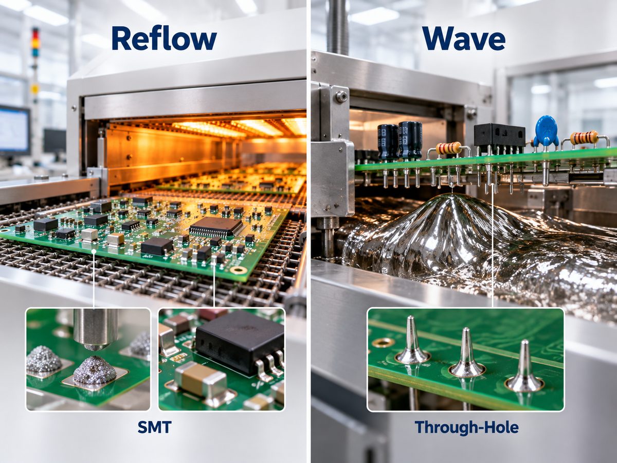
Comparison of reflow soldering for SMT and wave soldering for through-hole assembly
Factor Reflow Soldering Wave Soldering
Main component type SMT Through-hole
Solder source Printed solder paste Molten solder bath
Heating method Controlled reflow oven PCB passes over solder wave
Fine-pitch SMT Well suited Generally unsuitable
Typical production use SMT assembly THT assembly
Joint formation Paste melts on individual pads Exposed joints contact molten solder

Mixed-technology PCBAs may use both processes. SMT components can be reflowed first, followed by wave or selective soldering for through-hole components that cannot be processed during the SMT reflow stage.

The correct choice therefore depends less on which process is “better” and more on the component technology, PCB layout, heat sensitivity, production volume, and assembly sequence.

FAQs About Reflow Process Soldering

1. Which is the second stage in the reflow soldering process?

If the question refers to the four thermal stages inside a reflow oven, the second stage is the soak stage, following preheat. In a complete SMT manufacturing workflow, however, manufacturers may divide and number printing, SPI, placement, reflow, and inspection differently.

2. What temperature is used for reflow soldering?

For SAC305 lead-free solder, peak temperatures commonly fall within roughly 230–260°C, depending on the solder paste and assembly. Sn63/Pb37 uses a lower thermal profile and may peak around 205–215°C. The solder paste TDS and measured board profile should take priority over a generic peak-temperature value.

3. What is Time Above Liquidus in reflow soldering?

Time Above Liquidus, or TAL, is the period during which the solder joint remains hotter than the alloy’s liquidus temperature. It must be long enough to achieve suitable melting and wetting without subjecting the assembly to unnecessary thermal exposure.

For SAC305 processes, a range around 30–100 seconds may be encountered depending on the solder paste, although the correct value remains paste- and assembly-specific.

4. What solder paste is used for reflow soldering?

Lead-free SAC305 is widely used in current electronics assembly. Other alloys are selected for lower temperature, reliability, cost, regulatory, or application-specific requirements. The flux system and powder size must also match the PCB, stencil, component pitch, storage conditions, and cleaning process.

5. Can through-hole components be reflow soldered?

Some through-hole components can be assembled using pin-in-paste or intrusive reflow, where solder paste is printed around or into plated through-holes before the component is inserted and reflowed.

The component must tolerate the thermal profile, and sufficient solder volume must be provided to achieve acceptable barrel fill. For many conventional through-hole assemblies, wave or selective soldering remains more practical.

6. What is the difference between wave soldering and reflow soldering?

Reflow soldering heats deposited solder paste and is mainly used for SMT assembly. Wave soldering moves the underside of the PCB across a controlled wave of molten solder and is mainly used for through-hole assembly. Mixed PCBAs may use reflow for SMT first and wave or selective soldering afterward.

How Can EBest Circuit Support Your Reflow Soldering Project?

If you are preparing a PCB or PCBA project and need support with soldering process requirements, assembly manufacturability, or production planning, send your Gerber files, BOM, and assembly requirements to sales@bestpcbs.com. Our engineering team can review the project before production and help identify process conditions that may affect solder-joint quality, component reliability, or assembly yield.
You may also like

Reflow Process Soldering — Complete Engineering Guide for Reliable PCB Assembly
Wednesday, February 11th, 2026

Reflow process soldering is one of the most widely used assembly techniques in modern electronics manufacturing. From consumer devices to automotive control modules, the reflow process soldering workflow allows engineers to achieve consistent joints, high throughput, and repeatable thermal control.

This guide explains the full workflow in practical engineering terms, including equipment selection, temperature phases, alloy choices, and troubleshooting methods used in real SMT production environments.

What Is the Reflow Process of Soldering?

Reflow process soldering is a thermal assembly method where solder paste is first printed onto PCB pads, components are placed, and then the entire board passes through a controlled heating profile. The solder paste melts, wets the pads and leads, and solidifies to form electrical and mechanical connections.

Unlike hand soldering, heat is not applied locally. Instead, the entire PCB follows a carefully designed temperature curve.

Key characteristics include:

  • Uniform heating across the assembly
  • Precise temperature ramp control
  • Compatibility with fine-pitch components
  • High automation suitability

The process is essential for modern surface-mount technology because it supports high-density layouts, micro-pitch packages, and large production volumes.

What Is the Reflow Process of Soldering?

What Is the Reflow Process of Soldering?

Why Is It Called Reflow Soldering?

The term “reflow” refers to the melting and flowing behavior of solder paste during heating. Before entering the oven, solder paste is in a semi-solid state containing metal particles and flux. As temperature rises above the alloy’s liquidus point, the solder melts and flows across the pad surface.

This flow action allows:

  • Surface tension to align components
  • Oxides to be removed by flux activation
  • Metallurgical bonding between lead and pad

After peak temperature, controlled cooling solidifies the joint, locking components into position.

What Equipment Is Used for Reflow?

A standard reflow process soldering line includes several interconnected machines. Each stage influences solder joint quality.

Typical equipment:

  • Stencil printer – applies consistent solder paste volume
  • SPI inspection system – checks paste height and coverage
  • Pick-and-place machine – positions components with precision
  • Reflow oven – creates the temperature profile
  • AOI system – verifies final joint integrity

Modern convection reflow ovens are divided into multiple heating zones. These zones gradually raise temperature rather than applying sudden thermal stress.

For advanced assemblies, nitrogen reflow ovens reduce oxidation and improve wetting, especially for fine-pitch components.

At What Temperature Does Solder Reflow?

The reflow temperature depends mainly on alloy composition. Engineers must distinguish between liquidus temperature and peak profile temperature.

Typical examples:

SAC305 lead-free alloy

  • Liquidus: ~217 °C
  • Peak profile: 235–245 °C

Sn63/Pb37 eutectic alloy

  • Liquidus: 183 °C
  • Peak profile: 205–215 °C
At What Temperature Does Solder Reflow?

The peak value must be high enough to ensure full melting but low enough to avoid damaging components or PCB materials. Excessive temperature can cause pad cratering, delamination, or component warpage.

What Are the 7 Steps of Soldering?

In modern SMT manufacturing, soldering is not a single action but a controlled sequence of operations. Each step influences joint strength, electrical stability, and long-term reliability. Whether used in prototype assembly or high-volume PCBA production, these seven stages form a structured workflow that engineers follow to maintain process consistency.

1. Surface Preparation and PCB Cleaning

Before any solder is applied, the PCB surface must be clean and free from oxidation, dust, or residual oils. Even microscopic contamination can prevent proper wetting during heating.

Common preparation practices include:

  • Plasma cleaning or alcohol wiping for prototypes
  • Controlled storage to avoid humidity absorption
  • Verifying pad finish quality such as ENIG, HASL, or OSP

Proper preparation ensures the solder spreads evenly instead of forming isolated beads or weak fillets.

2. Solder Paste Printing or Flux Application

For reflow assemblies, solder paste is deposited onto pads using a laser-cut stencil. Paste volume directly determines final joint shape and reliability.

Key considerations during this step:

  • Stencil thickness and aperture design
  • Printing pressure and speed
  • Paste viscosity and metal content

In manual or selective soldering, flux may be applied instead of paste to activate surfaces during heating.

3. Component Placement and Alignment

After printing, components are positioned onto the solder paste deposits. Automated pick-and-place machines use vision systems to achieve precise alignment, while prototypes may be placed manually.

Important factors include:

  • Correct polarity and orientation
  • Accurate placement height
  • Avoiding paste smearing during placement

Surface tension during reflow can self-align small components, but accurate initial placement greatly reduces defects.

4. Preheating Stage

Preheating gradually raises the temperature of the entire assembly. This stage evaporates solvents inside the paste and reduces thermal shock.

Typical engineering goals:

  • Uniform temperature distribution across large boards
  • Prevention of sudden expansion in multilayer PCBs
  • Early activation of flux chemistry

A controlled ramp rate, usually between 1 °C and 3 °C per second, prevents component cracking and solder splatter.

5. Reflow Heating and Solder Melting

During this stage, the temperature rises above the solder alloy’s liquidus point. The metal particles inside the paste melt and flow across the pad and component leads.

What happens physically:

  • Flux removes oxides from metal surfaces
  • Molten solder forms intermetallic bonds
  • Surface tension pulls components into alignment

Engineers closely monitor time above liquidus to ensure complete wetting without overheating sensitive components.

6. Controlled Cooling and Solidification

Cooling begins immediately after peak temperature. This phase determines the internal grain structure of the solder joint.

Why controlled cooling matters:

  • Rapid cooling may introduce thermal stress
  • Extremely slow cooling can create coarse grain structures
  • Balanced cooling produces strong, fatigue-resistant joints

Convection ovens often include dedicated cooling zones to stabilize the solidification process.

7. Inspection, Testing, and Quality Verification

The final step confirms that soldering produced reliable electrical and mechanical connections. Inspection methods vary depending on product complexity.

Typical verification tools:

  • AOI to detect bridges, tombstoning, or insufficient solder
  • X-ray inspection for hidden joints like BGA packages
  • Functional testing or ICT for electrical validation

Feedback from inspection loops back into earlier steps, allowing engineers to fine-tune paste volume, placement accuracy, and temperature profiles.

What Are the Phases of Reflow Soldering?

A reflow profile is divided into several thermal zones. Understanding these phases helps engineers fine-tune process stability.

Preheat Phase

Temperature rises gradually to avoid thermal shock. Solvents evaporate during this stage.

Typical ramp rate: 1–3 °C per second.

Soak Phase

The PCB temperature stabilizes between 150 °C and 180 °C. Flux activation begins, and temperature differences across the board reduce.

Reflow Phase

Temperature exceeds the alloy liquidus point. Solder melts and forms joints through wetting and surface tension.

Peak Phase

The highest temperature occurs briefly. Time above liquidus typically lasts 30–90 seconds.

Cooling Phase

Controlled cooling ensures strong grain structure. Rapid cooling may trap stress, while slow cooling can create large brittle grains.

Can You Reflow Without Flux?

Technically possible but rarely recommended.

Flux performs several essential roles:

  • Removes oxide layers from metal surfaces
  • Improves solder wetting
  • Prevents re-oxidation during heating

Without flux, solder may ball up rather than spread. Joint reliability decreases significantly.

In specialized environments, such as vacuum or forming-gas atmospheres, fluxless reflow may be used. However, this requires advanced process control and is not common in standard SMT production.

What Is the 5 Ball Rule for Solders?

The “5 ball rule” is an informal guideline used during inspection. If multiple small solder balls appear around a joint, engineers evaluate whether they are cosmetic or reliability concerns.

General interpretation:

  • Fewer than five isolated solder balls may be acceptable depending on IPC standards.
  • Clusters or balls near fine-pitch leads indicate paste or profile issues.

Common causes include:

  • Excessive flux activation
  • Rapid temperature ramp
  • Contaminated PCB surface

Process tuning often resolves these defects.

Which Solder Is Better, 60/40 or 63/37?

Both alloys belong to traditional tin-lead systems but behave differently during melting.

60/40 – Sn60/Pb40

  • Melting range instead of single point
  • Slightly wider plastic state
  • More forgiving for manual soldering

63/37 – Sn63/Pb37

  • True eutectic alloy
  • Sharp melting point at 183 °C
  • Faster solidification and reduced cold joint risk

For automated reflow process soldering, Sn63/Pb37 generally provides better consistency due to its precise melting behavior. However, environmental regulations have pushed most production toward lead-free alloys like SAC305.

What Is the Difference Between Soldering and Reflow Soldering?

Traditional soldering and reflow soldering differ mainly in heat delivery method.

AspectTraditional SolderingReflow Process Soldering
Heat SourceLocalized iron or waveControlled oven profile
Assembly TypeThrough-hole or manual repairSurface-mount mass production
Process ControlOperator dependentAutomated and repeatable
Thermal UniformityLowHigh

Reflow provides higher throughput and consistency, which explains its dominance in modern electronics manufacturing.

FAQs

1. What Peak Temperature Should Be Used for SAC305 Reflow Process Soldering?

Most profiles target a peak between 235 °C and 245 °C. The exact value depends on board thickness, component sensitivity, and oven capability. Engineers often start with 240 °C and adjust based on wetting quality and component ratings.

2. Can a PCB Be Reflow Soldered Multiple Times Safely?

Yes, but the number of cycles should be limited. Excessive reflow passes may:

  • Degrade laminate integrity
  • Reduce pad adhesion strength
  • Increase risk of microcracking

High-Tg materials and proper cooling help maintain reliability when double-sided assembly requires multiple passes.

3. Why Do Solder Balls Appear After Reflow Process Soldering?

Solder balls usually indicate process imbalance. Common root causes include:

  • Too much solder paste volume
  • Rapid heating during preheat phase
  • Poor stencil release
  • Moisture or contamination on PCB surfaces

Adjusting ramp rate and stencil design often eliminates the issue.

4. How to Verify a Reflow Profile Without Expensive Profiling Tools?

Although professional thermocouple profilers offer the highest accuracy, smaller facilities can still validate profiles by:

  • Using temperature indicator labels
  • Comparing joint wetting appearance
  • Monitoring conveyor speed consistency
  • Checking for uniform solder fillets across large boards

These practical methods provide reasonable validation for low-volume production.

5. Does Nitrogen Atmosphere Improve Reflow Process Soldering Reliability?

Nitrogen reduces oxygen concentration in the oven, which enhances solder wetting and decreases oxidation. Benefits include:

  • Shinier solder joints
  • Reduced solder ball formation
  • Improved fine-pitch performance

However, nitrogen increases operational cost. Many manufacturers reserve it for high-density or high-reliability assemblies.

6. What Conveyor Speed Is Ideal for Small Batch Reflow Process Soldering?

There is no universal speed. Engineers typically adjust conveyor rate so total profile duration falls between 3 and 6 minutes. Thicker boards or heavy copper designs require slower speeds to ensure even heating.

You may also like

What Is Reflow Soldering Process? SMT Reflow Process
Friday, November 28th, 2025

The reflow soldering process is one of the most important steps in modern electronics manufacturing. It links every part of a PCB assembly line, from solder paste printing to final inspection. It also plays a direct role in reliability, long-term stability, and overall product success.

Today, reflow soldering is used for almost every surface mount component. It supports high-density PCBs, fine-pitch packages, micro-BGAs, CSPs, and modern compact devices that require precision.

What Is Reflow Soldering Process? SMT Reflow Process

What Is Reflow Soldering Process in Electronics Manufacturing?

The reflow soldering process is a thermal method used to attach electronic components to pads on a printed circuit board. During the process, solder paste is first applied to copper pads. Components are then placed on top of the paste. After that, the PCB assembly enters a reflow oven where the solder paste melts and forms permanent joints.

The key idea behind reflow process soldering is controlled heat. Every stage of the temperature profile is designed to move slowly and safely through heating zones. Each zone prepares the solder paste and components for the next transition.

Reflow soldering is especially popular because it supports high throughput. It is suitable for large-scale production lines and automated SMT assembly. It delivers reliable results with stable mechanical strength. It also allows manufacturers to assemble complex multi-layer boards with hundreds or thousands of components.

Another advantage is flexibility. The SMT reflow process works with leaded and lead-free solder paste. It also supports various PCB materials, including FR-4, aluminum substrates, flexible circuits, and hybrid boards. With optimized temperature control, it ensures excellent results even on sensitive components such as sensors, small chips, and delicate IC packages.

Which Steps Define the Reflow Soldering Process Step by Step?

The reflow soldering process step by step includes six main phases. Each phase contributes to the final solder joint formation. These steps must run in the correct order, with consistent timing and temperature control.

  • Step 1: Solder Paste Application

Every reflow soldering process begins with accurate paste printing. A stencil aligns with PCB pads, and solder paste is applied through stencil openings. The paste must be uniform.

  • Step 2: Component Placement

After paste printing, SMT components are placed using pick-and-place machines. These machines locate pads and place each part with high accuracy. The solder paste holds components temporarily due to its tackiness.

  • Step 3: Entry into the Reflow Oven

The PCB assembly enters the reflow oven on a conveyor. The oven includes multiple heating zones. Each zone has its own temperature and airflow control.

  • Step 4: Preheat and Soak Stages

As the assembly moves through the preheat zone, the board warms slowly. This step activates flux in the solder paste. It also prepares components for stronger wetting later. The soak zone equalizes PCB temperatures and ensures every part reaches similar thermal levels.

  • Step 5: Reflow Zone

Next, the PCB enters the zone where solder paste reaches peak reflow soldering temperature. At this moment, the solder melts and forms solid connections.

  • Step 6: Cooling Stage

Once melting occurs, the assembly moves into cooling zones. Proper cooling forms smooth, solid joints. A stable cooling rate prevents defects. When the solder hardens fully, the PCB becomes ready for inspection and testing.

Each stage in the SMT reflow process must be optimized. Even small changes can affect joint quality, component stability, or long-term reliability. When done correctly, however, the full process creates strong, durable, and dependable solder connections.

What Is the Composition of Solder Paste Used for Reflow Soldering Process?

Solder paste is a mixture of metal solder powder and flux. Both portions serve critical functions. Together, they enable clean wetting and strong mechanical bonding during the reflow soldering process.

The metal portion typically contains tin, silver, and copper for lead-free versions. Common formulas include SAC305 and SAC405. Leaded solder paste often uses Sn63/Pb37 for stable melting behavior. The spherical metal particles inside the paste make up about 85% to 90% of its total weight.

Flux is the second component. It removes oxides during heating. It also helps metal wet the pads smoothly. Flux mixtures include activators, resins, solvents, and additives. These improve paste stability and support proper printability.

BEST Technology select solder paste formulas based on application needs. Factors include melting point, wetting behavior, stencil thickness, PCB material, pad design, and component type. Proper paste guarantees cleaner joints and better strength.

Good solder paste also improves production efficiency. It prints smoothly, releases cleanly from stencils, and holds components in place. During heating, a high-quality formula creates bright and reliable solder joints with minimal voiding.

Without the right solder paste, the reflow process soldering workflow becomes harder to control. Therefore, paste selection is always a key step in surface mount production.

Which Is the Second Stage in the Reflow Soldering Process?

The second stage in the reflow soldering process is the component placement stage.

What Is Reflow Soldering Process? SMT Reflow Process

After solder paste application, the next job is placing components onto the PCB. Automated machines handle most of this work. These machines operate at high speed with precise accuracy. They inspect orientation and place each part exactly on its corresponding pad.

Component placement determines how well joints will form in later stages. Proper alignment lowers the risk of tombstoning, bridging, and misalignment defects.

During this stage, the tackiness of solder paste temporarily secures each component. This temporary hold is critical. It allows the PCB to travel safely through the reflow oven without parts shifting.

Which Zone Is the Lengthiest in the Reflow Soldering Process?

The lengthiest zone in the reflow soldering process is the soak zone.

This zone is designed to equalize temperatures across the entire PCB. It helps large components and small components reach similar heat levels. If the PCB does not heat uniformly, defects can occur later. Uneven heating can also impact solder wetting.

In the soak zone, the temperature rises slowly and stays stable for a controlled time. This period activates flux and prepares the solder paste for full melting. The soak zone is typically longer than the preheat or reflow zones because the board needs enough time to stabilize.

Its goal is simple: maintain consistent thermal balance. This balance reduces stress, lowers voiding risk, and improves overall solder quality.

What Is the Cooling Rate Suggested for Reflow Soldering Process?

The recommended cooling rate for the reflow soldering process ranges from 3°C to 4°C per second.

A controlled cooling rate is essential. Cooling too fast can lead to solder cracking. Cooling too slow can create dull joints or grainy structures. The goal is to solidify the molten solder smoothly with a uniform crystalline structure.

Proper cooling also enhances mechanical strength. When the solder cools at the right pace, joints become dense and stable. This stability supports long-term reliability even in high-stress environments such as automotive or industrial electronics.

Modern reflow ovens manage cooling using forced air or nitrogen. Both methods ensure fast and even temperature drops.

At Which Zone Is the Maximum Allowable Temperature of the Reflow Soldering Process Reached?

The maximum allowable temperature is reached in the reflow zone, also known as the peak zone.

This zone is the core of the SMT reflow process. Here, solder paste melts and flows. The entire PCB reaches the temperature necessary to form strong intermetallic bonds. Peak temperature depends on solder paste type but usually ranges from 235°C to 250°C for lead-free paste.

What Is Reflow Soldering Process? SMT Reflow Process

The peak zone must be precise. A temperature too high may damage components. A temperature too low prevents solder from melting fully.

During this stage, the molten solder wets the pads and forms solid joints. The duration of peak temperature exposure is short. Keeping it short protects components while still allowing proper melting. The reflow zone has the most impact on final solder quality.

How Does Wave Soldering Differ from Reflow Soldering Process?

Wave soldering and reflow soldering process are two different manufacturing methods. Both create solder joints, but they suit different component types.

Wave soldering is mainly used for through-hole components. In this process, the bottom of the PCB passes over a wave of molten solder. The wave touches exposed leads and forms joints instantly. This method works best for connectors, pin headers, and large leaded devices.

Reflow soldering is used mainly for surface mount components. In this method, solder paste is printed first. Components sit on the paste. The assembly then heats inside a reflow oven until the paste melts.

Here are the major differences:

  • Reflow soldering uses solder paste. Wave soldering uses molten solder waves.
  • Reflow is ideal for SMT. Wave is ideal for through-hole.
  • Reflow controls heat in multiple zones. Wave creates instant soldering in seconds.
  • Reflow supports fine-pitch components. Wave is better for larger parts.

Both processes remain important. Many PCBs use mixed technology. In such cases, manufacturers combine reflow soldering for SMT components and wave soldering for through-hole components.

Which Reflow Soldering Defects Appear Most Often?

Several reflow soldering defects may occur if the process is not well controlled. However, with optimized temperature profiles and proper solder paste handling, these issues can be greatly reduced.

Here are the defects that appear most often:

  • Tombstoning: One side of a small chip component lifts and stands upright. This occurs when pads heat unevenly.
  • Bridging: Two adjacent pads connect accidentally with excess solder. This defect happens when too much solder paste is applied or components shift during heating.
  • Insufficient Solder: There is not enough solder on a joint. This may result from poor paste printing or stencil wear.
  • Voiding: Trapped gases inside the solder joint create small holes. While some voiding is normal, too much can weaken mechanical strength.
  • Solder Balling: Small solder balls appear around pads. This defect often occurs when the paste splatters during reflow.
  • Cold Joint: A joint looks dull or grainy. This happens when solder does not melt properly or cooling is inconsistent.
  • Shifted Components: Components move out of position. Poor placement or low paste tackiness can cause this.

Modern reflow oven soldering process systems reduce most of these issues. Precise temperature control, optimized reflow soldering temperature profiles, and proper paste handling all help lower defect rates dramatically.

Why Is the SMT Reflow Soldering Process Used for Most PCBs?

The SMT reflow soldering process is used for most PCBs because it offers unmatched efficiency, precision, and reliability. It supports the fast pace of today’s electronics industry. It also fits the trend toward smaller, lighter, and more advanced products.

What Is Reflow Soldering Process? SMT Reflow Process

Several reasons make reflow the preferred choice:

  • 1. High Accuracy

Reflow soldering offers excellent alignment and precise solder volume control.

  • 2. High Productivity

Reflow ovens operate continuously. They handle large volumes with consistent performance.

  • 3. Strong Mechanical Reliability

Reflow solder joints display strong bonding strength. They tolerate vibration, thermal cycling, and long-term use.

  • 4. Supports Complex Boards

Modern multi-layer PCBs with complex designs rely on reflow soldering.

  • 5. Wide Component Compatibility

Reflow supports everything from tiny resistors to large ICs. Its versatility is unmatched.

  • 6. Lower Overall Cost

Automated reflow lines reduce labor cost and increase yield. This lowers total production cost.

  • 7. Excellent Thermal Control

Reflow ovens regulate every degree of temperature. This precision protects sensitive devices during assembly.

Conclusion:

The reflow soldering process is the foundation of modern PCB assembly. It supports small components, dense designs, and advanced electronics. Each stage—from paste printing to cooling—plays a vital role in forming reliable joints.

With proper paste selection, precise thermal profiles, and excellent process control, the SMT reflow process delivers durable and consistent results across all industries.

If you need further help or want to discuss reflow soldering in more detail, feel free to reach out anytime at sales@bestpcbs.com

You may also like