PCB manufacturing PCB manufacturing
Home > Blog

Best Low Volume PCB Assembly Manufacturer in China | Reliable Quality & Fast Delivery

March 18th, 2026

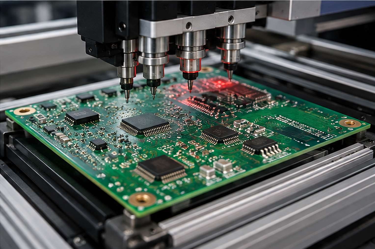
Struggling to find reliable low volume PCB assembly for small-batch projects? For teams navigating small-batch electronic production, consistent, high-quality low volume PCB assembly is often the biggest roadblock between prototype testing and full market launch.

EBest Technology delivers targeted low volume PCB assembly solutions to eliminate this gap entirely, with zero compromise on quality or speed. As a China-based professional manufacturer with 19+ years of dedicated PCBA expertise, we specialize in small-volume, prototype-focused assembly that skips strict mass-production minimums. We maintain strict quality controls and support fast turnaround for critical projects across medical, aerospace, and industrial equipment sectors. And we cut unnecessary delays and hidden costs, focusing on functional, compliant small-batch PCBA that meets global industry standards reliably.

Low Volume PCB Assembly, https://www.bestpcbs.com/blog/2026/03/best-low-volume-pcb-assembly/

What Are Low Volume PCB Assembly Services?

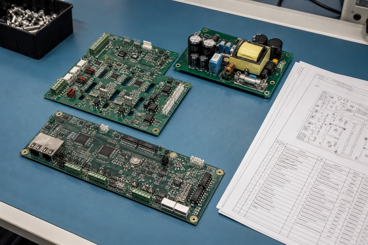
Low volume PCB assembly refers to specialized printed circuit board assembly services designed for small production runs, typically ranging from single prototype units to low thousands of finished boards, filling the critical gap between initial prototype development and full-scale mass manufacturing. Unlike mass production facilities that enforce high minimum order quantities (MOQs) and prioritize large-batch efficiency, this service caters to niche product testing, custom industrial equipment builds, medical device validation, aerospace component prototyping, and small-market product launches.

This targeted assembly model supports flexible order sizes, personalized production adjustments, and rigorous quality checks for every unit, making it ideal for projects that require precision, compliance, and speed without the expense of large-scale production. Every long tail keyword tied to small-batch assembly aligns with this core definition, including prototype PCB assembly services low volume and small volume PCB assembly.

Stuck Between Prototype and Mass Production? Our Services Are the Solution.

Finding reliable low volume PCB assembly is critical for bridging prototype and mass production. EBest provides targeted solutions for small-batch projects, with no high MOQs, strict quality controls, and fast turnaround. We serve medical, aerospace, and industrial equipment sectors, ensuring compliant, high-quality boards without unnecessary delays or hidden costs. Our in-house fabrication and component sourcing eliminate external supply chain risks, supporting seamless scaling from validation to limited production runs.

As a leading low volume PCB assembly manufacturer in China, EBest stands out with 19+ years of expertise, global certifications (ISO 13485, AS9100D, IATF 16949) and advanced automation. We offer a full range of services: prototype assembly, quick-turn solutions, full turnkey support, precision BGA, through-hole, flex/rigid-flex, and ceramic PCB assembly. Our capabilities include 13.2 million chips daily placement, 1-5 day standard lead times, and 24-hour rush service, with 100% full inspection before shipment. We also provide cost-saving strategies, such as consolidating small orders and using standard components, to optimize budgets without compromising quality.

Low Volume PCB Assembly, https://www.bestpcbs.com/blog/2026/03/best-low-volume-pcb-assembly/

Is Your Budget Tight? How to Save on Small Volume PCB Assembly?

Tight budgets often derail low volume circuit board assembly projects, from prototype validation to small-batch medical and industrial runs. Most teams overspend by 25%-35% on small orders, thanks to unoptimized workflows, hidden setup fees, and inflated middleman markups that punish low-quantity buyers.

Even small, one-off prototype batches face unfair premium pricing, and these extra costs quickly eat into project budgets and delay product development timelines for niche and specialized electronic builds.

As a professional China low volume PCB assembly factory, EBest cuts your total low volume PCB assembly costs by 20%-40% compared to standard manufacturers, with clear, actionable cost-saving methods. Our in-house PCB fabrication and direct component supply chain remove middleman fees entirely, slashing material and sourcing costs by 15%-20% for small batches.

We also optimize production setup and panelization for small orders, cutting per-unit setup and labor expenses by another 10%-20%, so you pay fair prices even for tiny batch sizes with no hidden charges.

We never sacrifice quality to lower costs, our streamlined small-batch workflows reduce waste and redundant steps, not performance. We offer free design-for-manufacturing (DFM) checks to avoid costly reworks, which can save you an extra 10%-15% on post-production fixes.

Our consistent, defect-controlled assembly also eliminates costly replacement orders, letting you stay within budget while getting reliable, production-ready boards for medical, aerospace, and industrial applications.

Does Low Volume Mean Lower Quality? Ensuring Excellence in Every Batch.

A common misconception about low volume PCB assembly services is that small batches mean lower quality standards, and this worry often stalls critical small-batch projects. At EBest, we eliminate this concern with strict, repeatable production controls and data-backed quality performance, tailored specifically for low volume and prototype orders.

We treat every small-batch order with the same rigorous process discipline as high-volume runs, with standardized operating procedures for every assembly step, no matter how small the order quantity. Our 19+ years of PCBA experience lets us lock in consistent quality without cutting corners or rushing production for quick turnaround.

We run full incoming material inspections for every batch, verifying raw PCB substrate quality and component authenticity before assembly starts. We only use A-grade, wear-resistant materials, and reject any subpar incoming parts to prevent defects early in the process.

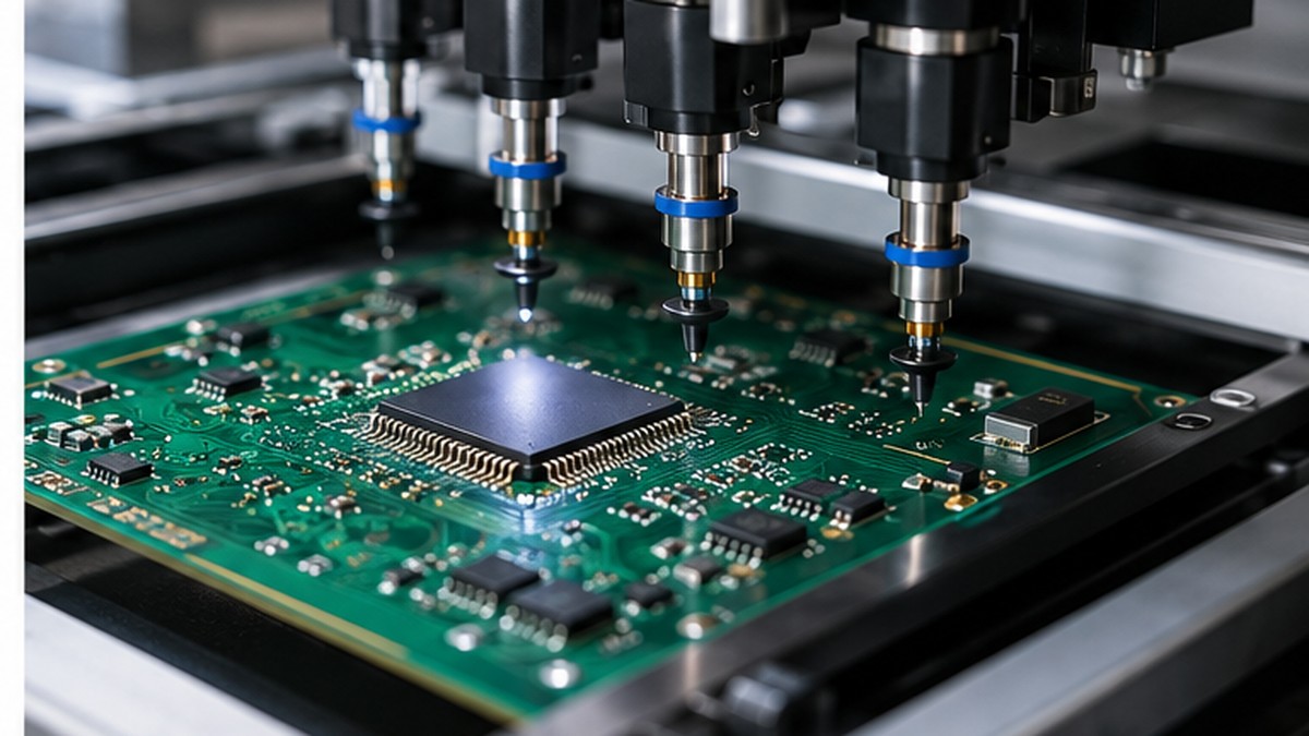
Our automated SMT placement equipment runs calibrated precision checks before each batch, maintaining consistent placement accuracy even for tiny 01005 SMD components and 0.25mm pitch BGA packages. This machine calibration eliminates human error and ensures uniform quality across every unit.

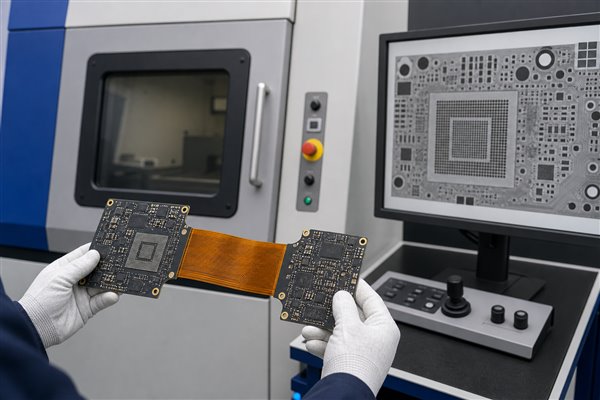
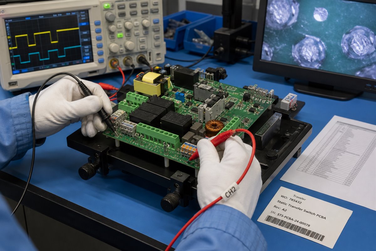
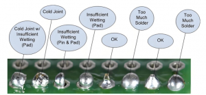
We enforce 100% full inspection on every assembled board before shipment, including automated optical inspection (AOI), soldering integrity checks, and functional performance testing where required. Our quality data confirms a defect rate of less than 0.3% for all low volume batches, matching the reliability of large-scale production.

Defective units are immediately isolated and reworked or scrapped, with zero substandard boards leaving our facility. We also conduct post-assembly stability checks for boards used in high-demand environments, ensuring long-term durability.

Our low volume assembly has been validated for real-world use across medical diagnostic tools, aerospace control components, and heavy-duty industrial equipment. These applications demand consistent, reliable performance, and our small-batch boards pass field testing and operational stress checks without quality gaps.

This track record proves low volume assembly never means lower quality, it simply means targeted, precise production that prioritizes consistency and reliability for your specialized, small-scale projects.

Urgent Need Assembled Boards? How We Accelerate Your Low Volume PCB Assembly

Missed deadlines for small-batch PCB orders can derail your entire project timeline, push back product launches, and even disrupt critical emergency operations. That’s why PCB assembly low volume orders need fast, dependable turnaround you can count on, not vague delivery promises.

EBest’s dedicated expedited production system delivers on urgent requests reliably: we can ship fully assembled, inspected boards within 24 hours for your most time-sensitive projects. Our in-house PCB fabrication and component sourcing teams cut out third-party delays entirely, and our automated assembly lines speed up processing without sacrificing placement precision or soldering quality.

For most standard low volume projects, our regular lead time is just 1–5 business days, far faster than industry averages for small-batch assembly. We’ve supported countless urgent requests: emergency medical device repairs, tight aerospace prototype testing windows, and last-minute industrial equipment replacement parts, helping clients hit critical deadlines without compromising on board quality.

Struggling with Parts? Our Component Sourcing for Circuit Board Assembly.

Few hurdles slow down low volume PCB assembly projects more than frustrating component sourcing struggles. Most buyers face endless hours hunting for small-batch parts, steep price markups for low-quantity orders, strict supplier MOQs that block small purchases, and constant fear of counterfeit or low-quality components derailing production entirely.

These roadblocks don’t just waste time, they push back project deadlines, inflate total costs, and create unnecessary stress for critical small-batch builds, from medical device prototypes to aerospace test components and industrial equipment replacements.

At EBest, we eliminate every one of these pain points with our dedicated, full-coverage component sourcing service, built exclusively to support low volume PCB assembly services and small-batch production needs. We take the entire parts procurement burden off your plate, so you can focus on project progress instead of supply chain headaches.

Our global, stable component supply chain covers every standard and specialty part you need, including SMD, BGA, QFN, QFP, and through-hole components, with no unfair small-order penalties. We vet every supplier rigorously to guarantee 100% authentic, high-quality components, eliminating counterfeit risks entirely for your sensitive industrial, medical, and aerospace projects.

We also leverage our 19+ years of industry partnerships to lock in competitive pricing for low-quantity parts, cutting your component costs by up to 20% compared to independent sourcing. No more haggling, no more delayed deliveries, and no more stalled production, just reliable, timely, cost-effective parts that keep your low volume PCB assembly project on track and on budget, from start to finish.

low volume circuit board assembly, https://www.bestpcbs.com/blog/2026/03/best-low-volume-pcb-assembly/

Why is a China-Based Factory Like EBest Your Best Choice?

Choosing a trusted low volume PCB assembly manufacturer in China means accessing cost efficiency, advanced technology, and global compliance, and EBest stands out as a leader with 19+ years of specialized experience. Below are the core advantages that make us the best partner for your small-batch PCBA needs:

  • 19+ years of dedicated PCB and PCBA manufacturing expertise, serving global clients across medical, aerospace, and industrial sectors
  • Full suite of global quality certifications (IATF 16949, ISO 9001, ISO 13485, AS9100D, RoHS, UL) for regulatory compliance.
  • In-house PCB fabrication and component sourcing, offering full turnkey solutions to streamline production.
  • No high MOQs, catering specifically to prototype, low volume, and small-batch assembly projects.
  • Advanced automated assembly equipment with 13.2 million chips daily placement speed for precision and speed.
  • 100% full inspection on every assembled board before shipment, zero quality shortcuts for small batches.
  • Expedited 24-hour rush service for urgent low volume orders, with standard 1-5 day lead times.
  • Monthly production capacity of 260,000 square feet, handling over 1,000 unique board designs monthly.
  • Customizable substrate and material options for ceramic, flex, rigid-flex, and high-frequency PCBs.
  • Dedicated personalized support team for every client, with end-to-end project tracking and transparency.

What Types of Low Volume PCB Assembly Services Does We Offer?

EBest offers a complete portfolio of low volume pcb assembly services to cover every small-batch and prototype need, with specialized support for unique board types and assembly requirements. Below are types of low volume PCB assembly services we offer you:

  • Prototype PCB Assembly: Custom prototype builds for design validation, testing, and regulatory approval across medical and aerospace industries.
  • Quick Turn PCB Assembly: Fast-turnaround small-batch assembly for urgent project deadlines and emergency replacement parts.
  • Full Turnkey PCB Assembly: End-to-end service including PCB fabrication, component sourcing, assembly, and full inspection.
  • BGA Assembly: Precision BGA assembly with 0.25mm minimum pitch, ideal for high-density industrial and aerospace electronics.
  • Through-Hole Assembly: Reliable through-hole component assembly for rugged industrial equipment and high-durability applications.
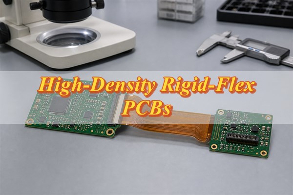
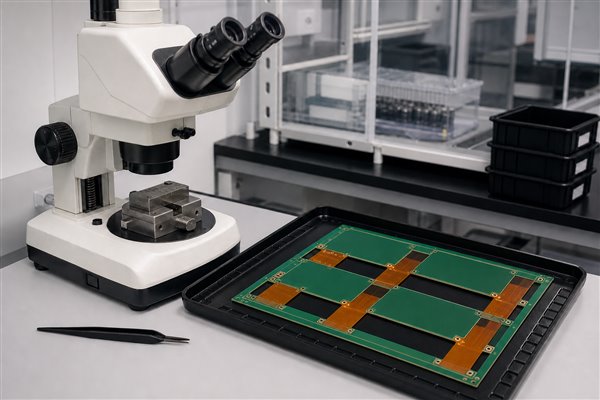
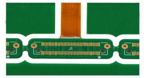
  • Flex & Rigid-Flex PCB Assembly: Specialized assembly for flexible circuit boards used in medical devices and compact aerospace components.
  • Ceramic PCB Assembly: High-temperature ceramic PCB assembly for industrial and aerospace applications with extreme operating conditions.
  • Box Assembly: Complete box build assembly with full automation and final inspection, ready for immediate deployment.
 Low Volume PCB Assembly Services, https://www.bestpcbs.com/blog/2026/03/best-low-volume-pcb-assembly/

Our Low Volume Circuit Board Assembly Capabilities

Capability CategoryDetailed Specifications
Placement Speed13,200,000 chips per day (automated precision placement)
Bare Board Size Range0.2″ x 0.2″ to 22″ x 47.5″
Minimum SMD Component01005 (ultra-small component support)
Minimum BGA Pitch0.25mm (high-density BGA assembly capability)
Max Component Size50mm x 150mm
Assembly TypesSMT, Through-Hole (THT), Mixed SMT+THT Assembly
Component PackagingReels, Cut Tape, Tube, Tray, Loose Parts
Standard Lead Time1-5 business days; 24-hour rush service available

How to Get a Quote for Your Small Volume PCB Assembly Project?

Securing a customized quote for your low volume PCB assembly project is simple and fully transparent with EBest. We’ve built a streamlined 4-step process to deliver accurate, fast pricing with zero hidden fees, so you know exactly what to expect before starting production. Follow these clear steps to launch your project smoothly:

  1. Submit Project Details: Send your complete PCB design files, including Gerber files, BOM list, and assembly drawings. Be sure to note your target order quantity, required lead time, and any special needs like unique substrate materials or custom assembly specs.
  2. Project Review & Feasibility Check: Our experienced production team reviews your design thoroughly, verifies component availability, and spots potential optimizations to improve quality or cut extra costs —no extra charge for this pre-production check.
  3. Custom Quote Delivery: We send a detailed, fixed quote that covers every cost: PCB fabrication, component sourcing, assembly, full inspection, and shipping. There are no surprise fees or added charges later, keeping your budget on track.
  4. Confirm Order & Start Production: Once you approve the quote and confirm all details, we immediately start production with full transparency, sending regular progress updates so you stay informed every step of the way.

Ready to get a hassle-free, customized quote for your low volume PCB assembly project? Don’t let budget uncertainty or project delays hold you back. Send us your project details today at sales@bestpcbs.com, and our team will respond quickly with a fair, detailed quote tailored to your needs. Whether you need prototype assembly, small-batch production, or urgent quick-turn services, we’re here to help you save costs, hit deadlines, and get reliable, high-quality boards every time.

FAQs About Low Volume Circuit Board Assembly

Q1: What is the minimum order quantity for low volume PCB assembly at EBest?
A1: We accept single prototype units, small-batch runs of 10-50 units, and mid-range low-volume orders up to a few thousand units. We cater specifically to clients who need small quantities without the high MOQs required by mass production manufacturers, making us ideal for prototype testing and niche product builds.

Q2: Are low volume PCB assembly orders subject to the same quality checks as high-volume orders?
A2: Yes, every low volume PCB assembly order undergoes 100% full inspection before shipment, including automated optical inspection (AOI), soldering quality checks, and functional testing where required. We follow the same certified quality protocols for all orders, regardless of size, and hold global certifications to ensure compliance for medical, aerospace, and industrial projects.

Q3: How long does it take to complete a standard low volume PCB assembly order?
A3: Our standard lead time for low volume PCB assembly is 1-5 business days from order confirmation. For urgent, time-critical projects, we offer a 24-hour expedited service for qualified small-batch orders, ensuring you receive finished boards exactly when you need them for testing or deployment.

Q4: Can you handle specialized PCB materials for low volume assembly?
A4: Absolutely, we support a full range of specialized PCB substrates and materials for low volume assembly, including FR4, ceramic, flex, rigid-flex, metal-based (MCPCB), and high-frequency materials. We customize substrate selection to match your project’s application, whether it’s high-temperature industrial equipment, compact medical devices, or aerospace-grade electronics.

Q5: Do you provide component sourcing for low volume orders with hard-to-find parts?
A5: Yes, our dedicated component sourcing team has a global, stable supply chain to source standard, specialized, and hard-to-find electronic components for low volume orders. We avoid counterfeit parts, secure competitive pricing even for small component quantities, and eliminate the hassle of independent parts procurement for your team.

You may also like

COB High-Power LED Module Copper Core PCB – High Thermal Conductivity for Brightness Stability

March 18th, 2026

Why Choose EBest for Your COB High-Power LED Module Copper Core PCB?

When you need a COB High-Power LED Module Copper Core PCB – High Thermal Conductivity for Brightness Stability, EBest is your first and best choice. Our products deliver unmatched performance to ensure your high-power LED modules operate reliably and stably.

Core parameters of our COB High-Power LED Module Copper Core PCB: Thermal conductivity up to 400 W/m·K, copper core thickness ranging from 0.8mm to 3.0mm, operating temperature range of -40°C to +125°C, dielectric layer thickness of 0.1mm to 0.3mm, and brightness stability deviation of ≤2% over 10,000 hours.

For consistent performance, reliable supply, and professional support, order your COB High-Power LED Module Copper Core PCB from EBest today—we provide the high-quality products your projects demand.

Copper Core PCB

Why Choose Us for COB High-Power LED Module Copper Core PCB?

Quality Assurance: Our COB High-Power LED Module Copper Core PCB undergoes strict multi-step testing (thermal shock, continuity, and insulation) to ensure its thermal conductivity and brightness stability meet global standards.

Lead Time Guarantee: We have a mature production line to ensure on-time delivery—standard orders ship within 7 to 10 days, and urgent orders can be fulfilled in 3 to 5 days without compromising quality.

Cost-Effectiveness: Through optimized supply chains and large-scale production, we reduce unnecessary costs, offering you high-quality COB High-Power LED Module Copper Core PCB at competitive prices.

Professional Service: Our technical team provides 24/7 support—from design consultation to after-sales troubleshooting, we assist you in resolving all issues related to your COB High-Power LED Module Copper Core PCB throughout the process.

Supply Chain Stability: We source high-purity copper and premium dielectric materials from trusted global suppliers, ensuring stable supply and consistent product quality for every batch.

What Are the Common Pain Points with COB High-Power LED Module Copper Core PCB, and How Does EBest Solve Them?

Many users encounter various performance-related issues when using COB High-Power LED Module Copper Core PCB—we address these pain points directly with proven solutions.

Pain Point 1: Poor thermal conductivity leading to module overheating and reduced brightness stability. Solution: We use high-purity copper cores and optimized dielectric layers to ensure a thermal conductivity of up to 400 W/m·K, effectively cooling LED modules and maintaining stable brightness.

Pain Point 2: Inconsistent product quality across batches. Solution: We conduct 100% full inspection on each COB High-Power LED Module Copper Core PCB to ensure every unit meets the same high standards.

Pain Point 3: Delayed deliveries disrupting production schedules. Solution: Through streamlined production processes and scientific inventory management, we ensure on-time delivery, even for large or urgent orders.

Pain Point 4: Lack of technical support for design and application. Solution: Our expert team offers free design consultations to help you optimize the design of your COB High-Power LED Module Copper Core PCB for your specific application scenario.

For hassle-free, high-performance COB High-Power LED Module Copper Core PCB, choose EBest—we turn your pain points into peace of mind.

COB High-Power LED Module Copper Core PCB – High Thermal Conductivity for Brightness Stability

What Is a COB High-Power LED Module Copper Core PCB, and Why Is It Critical for Brightness Stability?

A COB High-Power LED Module Copper Core PCB is a specialized circuit board with a copper core, designed specifically for mounting COB (Chip-on-Board) high-power LED modules. Its core function is efficient heat dissipation, which directly affects the brightness stability of LED modules.

High-power LED modules generate significant heat during operation. Without timely heat dissipation, LED chips will overheat, leading to dimming, color temperature shift, and shortened service life.

The copper core in our COB High-Power LED Module Copper Core PCB has excellent thermal conductivity, which quickly transfers heat generated by LED chips away, maintaining stable chip temperature and thus ensuring consistent brightness and long-term reliability.

How Does High Thermal Conductivity in COB High-Power LED Module Copper Core PCB Improve Brightness Stability?

High thermal conductivity in COB High-Power LED Module Copper Core PCB directly improves brightness stability by preventing LED chip overheating—the primary cause of brightness degradation in high-power LED modules.

When LED chips overheat, their light output decreases (known as “light decay”), and color temperature shifts, resulting in uneven brightness across the module.

Our COB High-Power LED Module Copper Core PCB has a thermal conductivity of up to 400 W/m·K, dissipating heat much faster than standard PCBs. This maintains a stable chip temperature, eliminates light decay, and ensures consistent brightness throughout the module’s service life.

What Key Specifications Should You Look for When Selecting a COB High-Power LED Module Copper Core PCB?

When selecting a COB High-Power LED Module Copper Core PCB, focus on the following critical specifications to ensure its performance is compatible with your LED modules.

  • Thermal Conductivity: Aim for ≥200 W/m·K (EBest products reach up to 400 W/m·K) to ensure effective heat dissipation.
  • Copper Core Thickness: 0.8mm to 3.0mm—thicker cores improve thermal performance for high-power applications.
  • Dielectric Layer: 0.1mm to 0.3mm with high insulation resistance to prevent short circuits and ensure safety.
  • Operating Temperature Range: -40°C to +125°C to withstand harsh working environments.
  • Brightness Stability: ≤2% deviation over 10,000 hours to ensure consistent performance over the long term.

What Advantages Does EBest’s COB High-Power LED Module Copper Core PCB Have Compared to Standard PCBs?

SpecificationEBest COB High-Power LED Module Copper Core PCBStandard FR-4 PCBAluminum Core PCB
Thermal ConductivityUp to 400 W/m·K1-2 W/m·K10-20 W/m·K
Brightness Stability≤2% deviation over 10,000 hours≥8% deviation over 10,000 hours≥5% deviation over 10,000 hours
Operating Temperature Range-40°C to +125°C-20°C to +85°C-30°C to +105°C
DurabilityHigh (resistant to thermal shock and vibration)Low (prone to warping under heat)Medium (better than FR-4 but inferior to copper core)
Compatibility with High-Power LEDsIdeal (handles modules above 50W)Not recommended (overheats quickly)Suitable for 10-50W modules

Which Industries Benefit Most from COB High-Power LED Module Copper Core PCB?

The COB High-Power LED Module Copper Core PCB is essential for industries that rely on high-power LED modules and pursue stable brightness and long-term reliability. Below are four key industries and real EBest case studies.

1. Industrial Lighting

Industrial warehouses and factories use high-power LED modules for bright, uniform lighting. Our COB High-Power LED Module Copper Core PCB ensures stable brightness even in high-temperature environments.

Case Study: A global industrial lighting manufacturer used our PCB for 200W LED high bay lights. The results showed: 30% less heat buildup and 98% brightness stability over 20,000 hours.

2. Architectural Lighting

Architectural lighting requires precise brightness control for building facades and public spaces. The high thermal conductivity of our PCB prevents color temperature shift and maintains lighting uniformity.

Case Study: An architectural firm used our COB High-Power LED Module Copper Core PCB for a 100-square-meter building facade project. The PCBs delivered uniform brightness with no visible light decay for 18 months.

3. Automotive Lighting

Automotive headlights and taillights use high-power LEDs, requiring PCBs that can withstand extreme temperature fluctuations. Our PCB can adapt to a temperature range of -40°C to +125°C, ensuring reliable operation in all climates.

Case Study: An automotive supplier used our PCB for LED headlights. After 10,000 thermal cycle tests (from -40°C to +85°C), the PCBs still maintained stable brightness and performance.

4. Outdoor Flood Lighting

Outdoor floodlights operate in harsh conditions (rain, extreme heat/cold) and require long-lasting brightness. Our COB High-Power LED Module Copper Core PCB is moisture-resistant and maintains stable thermal efficiency.

Case Study: A municipal government used our PCB for 150W outdoor floodlights. The PCBs delivered consistent brightness for 2 years with no maintenance issues.

How to Design a COB High-Power LED Module Copper Core PCB for Maximum Brightness Stability?

Designing a COB High-Power LED Module Copper Core PCB for maximum brightness stability requires focusing on thermal management, material selection, and layout design—here’s how to do it.

Choose the Right Copper Core Thickness

For high-power LED modules above 50W, we recommend using a 1.5-3.0mm copper core. Thicker cores improve heat dissipation, reduce LED chip temperature, and maintain brightness stability.

Optimize the Dielectric Layer Design

Use a high-insulation, thermally conductive dielectric layer (0.1-0.3mm). This ensures electrical safety while quickly transferring heat from LED chips to the copper core.

Optimize Layout for Heat Dissipation

Evenly distribute LED chips across the PCB surface to avoid heat concentration; use large copper pads and thermal vias to transfer heat from the chip surface to the copper core.

Partner with a Reliable Manufacturer

Work with a manufacturer like EBest that specializes in COB High-Power LED Module Copper Core PCB. We offer design support to optimize your layout for maximum brightness stability.

What Quality Certifications Does EBest’s COB High-Power LED Module Copper Core PCB Have?

EBest’s COB High-Power LED Module Copper Core PCB meets global quality standards and holds multiple industry-recognized certifications. Below is a complete list of our certifications.

Certification NameCertification BodyRelevance to COB High-Power LED Module Copper Core PCB
ISO 9001:2015ISO (International Organization for Standardization)Ensures stable quality management and production processes
UL 94 V-0UL (Underwriters Laboratories)Fire-resistant, critical for LED modules in enclosed spaces
IPC-6012IPC (Association Connecting Electronics Industries)Meets rigid PCB performance standards for high-power applications
RoHSEuropean Union (EU)Environmentally friendly, free of hazardous substances
REACHEuropean Union (EU)Complies with EU chemical safety standards for global distribution

What Services Does EBest Offer for COB High-Power LED Module Copper Core PCB?

EBest provides end-to-end services for COB High-Power LED Module Copper Core PCB, from design to delivery, to ensure your project progresses seamlessly.

  • Free Design Consultation: Our expert team helps you optimize your PCB design to enhance thermal conductivity and brightness stability.
  • Rapid Prototyping: Complete prototyping in 3-5 days, allowing you to test the performance of your COB High-Power LED Module Copper Core PCB before mass production.
  • Mass Production: Scalable production capacity to meet large-order requirements while ensuring consistent quality.
  • Quality Inspection: 100% full inspection (thermal shock, continuity, insulation) for every PCB.
  • After-Sales Support: 24/7 technical support to resolve any issues you encounter during PCB use.

How to Test the Thermal Conductivity of a COB High-Power LED Module Copper Core PCB?

Testing the thermal conductivity of your COB High-Power LED Module Copper Core PCB is a critical step to ensure it meets your project requirements. Follow these simple steps.

Step 1: Gather Test Equipment

You will need a thermal conductivity tester, temperature sensor, power supply, and your COB High-Power LED Module Copper Core PCB sample.

Step 2: Prepare the Sample

Cut the PCB into a standard size (100x100mm) and clean the surface to remove any debris that could affect heat transfer.

Step 3: Conduct the Test

Place the sample in the thermal conductivity tester, apply a stable heat source, measure the temperature difference across the PCB, and calculate using the formula: Thermal Conductivity = (Heat Flux × Thickness) ÷ Temperature Difference.

Step 4: Verify the Results

Compare the test result with your required specification (≥200 W/m·K for high-power applications). EBest’s PCBs are pre-tested, so you can trust they meet the stated thermal conductivity.

What Are the Common Myths About COB High-Power LED Module Copper Core PCB?

There are many misconceptions about COB High-Power LED Module Copper Core PCB—we debunk the most common ones to help you make informed decisions.

Myth 1: Copper Core PCBs Are Too Heavy for LED Modules

Fact: Our COB High-Power LED Module Copper Core PCB uses lightweight, high-purity copper cores (0.8-3.0mm) that are light enough for most LED module applications, including portable lighting.

Myth 2: High Thermal Conductivity Isn’t Necessary for Small LED Modules

Fact: Even small high-power LED modules (above 50W) generate enough heat to cause light decay. A copper core PCB ensures brightness stability, regardless of module size.

Myth 3: Copper Core PCBs Are Difficult to Manufacture

Fact: EBest has optimized production processes to efficiently manufacture COB High-Power LED Module Copper Core PCB, ensuring consistent quality and fast lead times.

Myth 4: Aluminum Core PCBs Perform as Well as Copper Core PCBs

Fact: Aluminum core PCBs have a thermal conductivity of only 10-20 W/m·K, much lower than the maximum 400 W/m·K of copper core PCBs, making them less effective for high-power LED modules.

FAQ: Common Questions About COB High-Power LED Module Copper Core PCB

Below are the most frequently asked questions about COB High-Power LED Module Copper Core PCB, with clear, direct answers to help you solve problems quickly.

Q1: How Long Does a COB High-Power LED Module Copper Core PCB Last?

A1: Under normal operating conditions (-40°C to +125°C), EBest’s COB High-Power LED Module Copper Core PCB has a service life of more than 50,000 hours. This matches the service life of high-power LED modules, ensuring no premature failure.

Q2: Can COB High-Power LED Module Copper Core PCB Be Customized to Specific Sizes?

A2: Yes, we offer fully customized COB High-Power LED Module Copper Core PCB in any size (from 50x50mm to 500x500mm) and thickness (0.8-3.0mm) to match your LED module design.

Q3: Does the COB High-Power LED Module Copper Core PCB Require Special Mounting?

A3: No, our COB High-Power LED Module Copper Core PCB uses standard mounting holes and dimensions, making it compatible with most LED module enclosures and fixtures. We can also customize mounting holes if needed.

Q4: How Does EBest Ensure Consistent Brightness Stability in Every PCB?

A4: Before shipping, we test every COB High-Power LED Module Copper Core PCB for thermal conductivity and brightness stability. Our quality control process includes thermal shock testing and brightness deviation measurement to ensure ≤2% deviation over 10,000 hours.

Q5: Can the COB High-Power LED Module Copper Core PCB Be Used for Outdoor Applications?

A5: Yes, our PCB is designed for outdoor use—it is moisture-resistant, corrosion-resistant, and can withstand extreme temperature fluctuations (-40°C to +125°C), making it ideal for outdoor floodlights and architectural lighting.

Q6: What Is the Minimum Order Quantity for COB High-Power LED Module Copper Core PCB?

A6: We accept small orders (minimum 10 units) for prototyping and large orders (1,000+ units) for mass production. This flexibility makes us suitable for both small projects and large-scale manufacturing.

Q7: How Quickly Can EBest Deliver Custom COB High-Power LED Module Copper Core PCB?

A7: Custom prototypes are delivered in 3-5 days, and standard custom orders are delivered in 7-10 days. Urgent orders can be fulfilled in 2-3 days with prior arrangement.

What Are the Latest Innovations in COB High-Power LED Module Copper Core PCB?

The COB High-Power LED Module Copper Core PCB industry is constantly evolving, with new innovations to improve thermal conductivity, brightness stability, and sustainability.

Innovation 1: Advanced Copper Alloys—We use high-purity copper alloys to boost thermal conductivity up to 400 W/m·K, improving heat dissipation and brightness stability.

Innovation 2: Thin-Film Dielectric Layers—New thin-film dielectric materials reduce thermal resistance, transferring heat faster from LED chips to the copper core.

Innovation 3: Sustainable Manufacturing—We use eco-friendly materials and processes to produce COB High-Power LED Module Copper Core PCB that meet RoHS and REACH standards, reducing environmental impact.

Why Is EBest the Trusted Supplier for COB High-Power LED Module Copper Core PCB?

EBest is the trusted supplier for COB High-Power LED Module Copper Core PCB because we combine quality, reliability, and expert support to meet your project needs.

We have years of experience manufacturing high-performance PCBs for high-power LED modules, with a proven track record of serving global clients in the industrial, architectural, automotive, and outdoor lighting industries.

Our commitment to quality, on-time delivery, and 24/7 support makes us the top choice for businesses that demand the best COB High-Power LED Module Copper Core PCB for brightness stability and thermal performance.

We provide high-quality COB High-Power LED Module Copper Core PCB – High Thermal Conductivity for Brightness Stability. If you need reliable, high-performance PCBs for your LED modules, please place your order with EBest. Our email is sales@bestpcbs.com, and our team is ready to assist you with all your requirements.

You may also like

LED Sign Board Light Aluminum PCB Solutions for Outdoor Advertising

March 18th, 2026

LED Sign Board Light Aluminum PCB is the core technology behind modern illuminated signage, delivering superior heat dissipation, longer lifespan, and stable brightness. This article explains how to design, manufacture, and optimize LED aluminum PCB sign boards for reliable and scalable applications.

EBest Circuit (Best Technology) is a specialized MCPCB manufacturer of LED Sign Board Light Aluminum PCB, with over 20 years of experience in thermal management and outdoor lighting applications. We focus on delivering high-reliability aluminum PCBs designed for harsh environments, offering strong waterproof performance, UV resistance, and stable heat dissipation to ensure long-term operation of outdoor advertising systems. Our engineering team optimizes thermal conductivity and circuit layout to maintain consistent brightness and prevent light decay, helping your LED signage stand out with uniform illumination. With in-house fabrication, assembly, and strict quality control systems, we ensure stable batch consistency and reliable supply for large-scale projects. From material selection to final testing, every step is engineered to meet the demanding requirements of outdoor LED sign boards. Pls feel free to call us anytime at +86-755-2909-1601 to discuss your LED aluminum PCB project.

LED Sign Board Light Aluminum PCB

Why Choose a Reliable LED Sign Board Light Aluminum PCB Manufacturer?

LED Sign Board Light Aluminum PCB requires strict control of thermal performance, soldering quality, and long-term reliability. EBest Circuit (Best Technology) provides a complete solution from PCB fabrication to assembly, ensuring stable LED brightness and extended service life.

Core Parameters You Should Care About:

  • Thermal conductivity: 1.0–3.0 W/m·K (standard aluminum base)
  • Copper thickness: 1–3 oz for high current LED circuits
  • Board thickness: 1.0–1.6 mm aluminum substrate
  • Surface finish: HASL / ENIG for stable soldering
  • Operating temperature: -40°C to 125°C

Why choose EBest Circuit (Best Technology)?

  • Quality: Strict AOI + X-ray inspection ensures stable LED solder joints
  • Lead time: Fast turnaround within 1.5 weeks for PCBA
  • Service: professional engineering team supports full lifecycle optimization
  • Supply chain: Integrated sourcing avoids component shortages

If you are sourcing LED Aluminum PCB Sign Light Board, working with a vertically integrated manufacturer significantly reduces risk and improves product consistency. You are warmly welcome to contact us at sales@bestpcbs.com to arrange a factory visit.

LED Sign Board Light Aluminum PCB

What Is an LED Light PCB and Why Use Aluminum Substrate?

LED Light PCB is a circuit board designed specifically to power and control LED components. Aluminum PCBs are preferred because they dissipate heat efficiently, preventing LED degradation.

Key advantages:

  • Excellent heat transfer from LED junction to base
  • Improved LED lifespan and brightness consistency
  • Reduced risk of thermal runaway
  • Compact design for LED sign boards

How Does Aluminum PCB Improve LED Sign Board Performance?

The answer is simple: thermal management. Heat is the primary failure factor in LED sign boards.

Performance comparison:

ParameterFR4 PCBAluminum PCB
Thermal conductivity0.3 W/m·K1.0–3.0 W/m·K
LED lifespanLowerHigher
Heat dissipationPoorExcellent
ReliabilityModerateHigh

This is why Aluminum Board LED PCB Sign Light dominates outdoor and high-brightness signage.

What Services and Certifications Do We Provide for LED Aluminum PCB Sign Light Board?

CategoryDetails
PCB FabricationAluminum PCB, MCPCB, multi-layer LED boards
AssemblySMT, DIP, automated through-hole assembly
TestingAOI, X-ray, functional testing
CertificationsISO9001, ISO13485, IATF16949, AS9100D
TraceabilityMES system with 5-second tracking

What Are the Most Common Challenges in LED Sign Board Aluminum PCB Projects?

Many users face similar issues when developing LED Sign Light Aluminum PCB Board.

Typical challenges:

  • Uneven brightness across LED arrays
  • Overheating leading to early failure
  • Poor soldering reliability on aluminum base
  • Design not optimized for manufacturability
  • Inconsistent supply quality

How we solve them:

  • Thermal simulation and optimized copper layout
  • Controlled reflow profiles for aluminum substrates
  • DFM analysis before production
  • Stable component sourcing system

Looking for a stable pcb led solution? EBest Circuit (Best Technology) ensures consistency from prototype to volume production.

How to Design an Efficient LED Sign Board Light Aluminum PCB?

Design is the foundation of performance. A well-designed Led board sign ensures uniform light output and long-term reliability.

Design guidelines:

  • Use wide copper traces for current distribution
  • Ensure uniform LED spacing
  • Optimize thermal vias (if multilayer)
  • Avoid hotspots through balanced layout

How Is LED Aluminum PCB Manufactured Step by Step?

The quality of an LED aluminum PCB depends on process control at every stage, especially for single-sided thermoelectric separation copper-base boards. The full workflow is divided into panel fabrication and baseboard fabrication, followed by lamination and finishing.

Panel Fabrication Process

The panel defines the electrical circuit and current path. Its precision directly impacts LED brightness uniformity and reliability.

Process flow:

Cutting
Raw material is cut into production panels with controlled size and edge quality.

Baking
Panels are baked to remove moisture and stabilize material performance.

Circuit Formation
Circuit patterns are transferred onto copper, defining pads and traces.

Circuit QC (Visual Inspection)
Quick inspection to identify obvious defects like misalignment or missing patterns.

Etching
Unwanted copper is removed, forming the final circuit layout.

Etching QC (Visual + AOI + Testing)
Multi-level inspection ensures circuit integrity and detects opens/shorts early.

PP Lamination (Pure Glue)
Adhesive layer is applied for bonding with the aluminum base.

Drilling / Targeting
Positioning holes are created to ensure alignment accuracy.

Routing Slot (Boss Position)
Mechanical routing defines the convex platform structure.

Pending Lamination (Panel & Baseboard)
Panel is prepared and ready for bonding with the baseboard.

Baseboard Fabrication Process

The baseboard provides mechanical strength and heat dissipation. This stage ensures thermal stability and surface protection.

Process flow:

Cutting
Aluminum base is cut to required size.

Single-Side High-Temperature Film (If Needed)
Protective film is applied if not pre-coated.

Board Grinding
Surface is refined to improve adhesion and flatness.

Circuit Boss Formation (Dry Film / Wet Film)
Convex structure is formed for thermoelectric separation.

Etching
Material is etched to define structure and copper features.

Lamination (Panel & Baseboard)
Panel and baseboard are bonded—this is the key structural step.

Film Stripping
Temporary films are removed after lamination.

Targeting
Alignment is rechecked for accuracy.

Board Grinding
Surface is refined again for better coating performance.

Solder Mask (Standing → Baking → Exposure → Developing)
Protective layer is applied to prevent oxidation and short circuits.

Solder Mask QC
Inspection ensures proper coverage and alignment.

Legend Printing
Text and markings are added for identification.

Baking Cure
Final curing strengthens coatings and improves durability.

Surface Finish (OSP / ENIG / ENEPIG / Lead-Free HASL)
Surface treatment ensures solderability and corrosion resistance.

Profiling (Drilling / V-CUT / Routing)
Final board shape is defined.

Testing
Electrical testing verifies circuit performance.

FQC
Final inspection checks overall appearance and structure.

FQA
Quality assurance confirms readiness for shipment.

Vacuum Packaging
Boards are sealed to prevent moisture and contamination.

Warehousing
Products are stored with traceability.

Shipment
Finished boards are delivered to customers.

Why This Process Matters for LED Sign Boards

Each step ensures that the LED Sign Board Light Aluminum PCB delivers:

  • Stable heat dissipation
  • Consistent brightness
  • Strong structural bonding
  • Reliable outdoor performance

A well-controlled process is the foundation of long-lasting LED signage.

What Industries Use LED Aluminum PCB Sign Boards the Most?

LED letter sign board applications are expanding rapidly across industries.

IndustryApplication
AdvertisingOutdoor signage, billboards
RetailStorefront LED sign boards
AutomotiveLED lighting modules
Smart cityTraffic signals, display panels

How to Ensure Long-Term Reliability of LED Sign Light Aluminum PCB Board?

Reliability depends on materials, process, and testing.

Key factors:

  • High thermal conductivity dielectric layer
  • Stable solder joints with controlled reflow
  • Proper coating for outdoor protection
  • Full functional testing

How Does Automated Through Hole Assembly Improve LED PCB Quality?

Automation ensures consistency and reduces human error.

Benefits:

  • Higher production efficiency
  • Stable solder quality
  • Reduced defect rates

What Are the Key Differences Between LED PCB Types?

TypeApplicationAdvantage
FR4 PCBLow-power LEDLow cost
Aluminum PCBHigh-power LEDThermal performance
Ceramic PCBExtreme conditionsBest thermal stability

How to Choose the Right LED Aluminum PCB Manufacturer?

Choosing the right partner directly impacts product quality.

Selection criteria:

  • Experience in LED PCB manufacturing
  • Full in-house production capability
  • Strong engineering support
  • Certifications and traceability systems
LED Sign Board Light Aluminum PCB

If you are looking for a reliable LED Sign Board Light Aluminum PCB manufacturer, EBest Circuit (Best Technology) provides complete solutions from design to assembly. Pls feel free to contact us anytime at sales@bestpcbs.com to start your project with a trusted partner.

FAQs About LED Sign Board Light Aluminum PCB

What is LED Sign Board Light Aluminum PCB?
It is a metal-core PCB designed to support LED lighting with efficient heat dissipation and stable performance.

Why use aluminum PCB for LED signs?
Aluminum improves thermal management, extending LED lifespan and maintaining brightness.

What thickness is best for LED aluminum PCB?
Typically 1.0–1.6 mm depending on application and thermal requirements.

How to improve LED PCB heat dissipation?
Use high thermal conductivity materials, optimize copper layout, and ensure proper mounting.

What surface finish is best for LED PCB?
ENIG provides better reliability, while HASL is cost-effective for standard applications.

Can aluminum PCB support high current LEDs?
Yes, with proper copper thickness and thermal design.

You may also like

Factors to Consider When Choosing Ceramic Substrates

March 18th, 2026

Understanding factors to consider when choosing ceramic substrates is critical for device performance and reliability. This guide covers all essential factors to consider when choosing ceramic substrates for professional engineering applications.

Ceramic Substrates

What are the key factors to consider when choosing ceramic substrates?

The most important factors include thermal, electrical, mechanical, material, and application compatibility.

These elements directly decide performance, stability, and service life.

Selecting correctly avoids failures in high‑demand environments.

  • Thermal conductivity and thermal expansion
  • Dielectric constant and insulation performance
  • Mechanical strength and structural stability
  • Material type and manufacturing compatibility
  • Quality, supply chain, and delivery

How do material properties affect ceramic substrate selection?

Material properties form the foundation of ceramic substrate performance.

Mismatched properties lead to overheating, signal loss, or mechanical breakage.

Each parameter must align with your application needs.

Thermal conductivity requirements

Higher thermal conductivity improves heat dissipation for high‑power devices.

It keeps components cool and extends service life.

This is non‑negotiable for power and automotive electronics.

Dielectric and insulation performance

Dielectric constant impacts signal integrity.

High insulation prevents leakage in high‑voltage systems.

Low dielectric loss improves energy efficiency.

Which thermal factors matter most for ceramic substrates?

Thermal performance ensures long‑term stability under load and temperature cycles.

Poor thermal design causes cracking, warping, and early failure.

Thermal matching is vital for reliable assembly.

  • Coefficient of thermal expansion (CTE) matching
  • Thermal cycling stability
  • High temperature resistance
  • Heat dissipation path design
  • Compatibility with thermal interface materials

How to match electrical requirements for ceramic substrates?

Electrical properties protect circuits and ensure signal quality.

They prevent interference and breakdown in demanding environments.

Correct values keep systems safe and stable.

Insulation resistance

High insulation resistance supports high‑voltage applications.

It reduces risk of short circuits and electrical failures.

Critical for power electronics and industrial controls.

Dielectric loss

Low dielectric loss improves efficiency in high‑frequency devices.

It reduces heat from signal transmission.

Ideal for communication and server equipment.

What mechanical standards should ceramic substrates meet?

Mechanical strength prevents breakage during production and use.

It supports handling, assembly, and harsh environments.

Strong substrates maintain dimensional stability.

  • Bending strength
  • Fracture toughness
  • Hardness and wear resistance
  • Dimensional accuracy
  • Thermal shock resistance

How to compare common ceramic substrate materials

How to compare common ceramic substrate materials?

The table below helps you choose based on performance and application.

MaterialThermal Conductivity (W/m·K)Dielectric ConstantTypical Applications
Alumina (Al₂O₃)20–309.8Consumer electronics, LED
Aluminum Nitride (AlN)170–2308.8Automotive, power electronics
Silicon Nitride (Si₃N₄)20–907.0High‑power devices
Zirconia (ZrO₂)2–325.0Medical devices, sensors

Which industries use ceramic substrates most widely?

Ceramic substrates perform best in four high‑growth industries.

Automotive electronics

AlN substrates handle heat in EV power modules.

They withstand vibration and extreme temperatures.

Ensure stable performance in motor controls.

Medical electronics

High‑purity alumina offers biocompatibility and insulation.

It meets strict medical standards for monitoring devices.

Safe for long‑term implantable and diagnostic tools.

LED & power electronics

Ceramic substrates improve heat dissipation for LEDs.

They extend lifespan and boost brightness.

Widely used in industrial and outdoor lighting.

Aerospace & industrial control

Special ceramics resist extreme temperatures and corrosion.

They meet aerospace reliability standards.

Stable in automation and harsh factory environments.

How to ensure processing compatibility of ceramic substrates?

Processing compatibility lowers production difficulty and cost.

Good metallization and bonding support strong assembly.

Stable processing ensures consistent yields.

  • Machinability
  • Metal layer adhesion
  • Solderability and bonding strength
  • Compatibility with standard PCB processes
  • Tolerance control

How to judge ceramic substrate quality and reliability?

Quality control prevents inconsistent performance and failures.

Certified materials and testing ensure long service life.

Reliable substrates reduce maintenance and replacement cost.

  • Raw material purity
  • Dimensional accuracy
  • Thermal cycle testing
  • Insulation and voltage testing
  • Compliance with international standards

Why supply chain & delivery matter for ceramic substrates?

Stable supply avoids production delays and shortages.

On‑time delivery keeps projects on schedule.

Consistent quality supports mass production.

  • Steady raw material supply
  • On‑time delivery capability
  • Full quality traceability
  • Professional technical support
  • Mass production capacity

Can ceramic substrates be customized for special uses?

Customization meets unique design and performance needs.

Tailored materials, sizes, and structures fit special equipment.

Custom solutions improve overall device efficiency.

  • Custom material formulas
  • Special thickness and shape
  • Modified thermal or electrical properties
  • Application‑specific metallization
  • Unique packaging requirements

FAQ: Top questions about factors to consider when choosing ceramic substrates

What factors to consider when choosing ceramic substrates?

Key factors include thermal performance, electrical properties, mechanical strength, material type, quality, supply chain, and application compatibility.

Which ceramic substrate is best for high power?

Aluminum nitride (AlN) is best for high power due to ultra‑high thermal conductivity.

How to ensure thermal reliability of ceramic substrates?

Match thermal expansion coefficients and use high‑thermal‑conductivity materials.

What is the difference between AlN and alumina substrates?

AlN has much higher thermal conductivity; alumina offers cost‑effective general use.

Can ceramic substrates be used in medical devices?

Yes, high‑purity alumina is widely used for biocompatibility and stability.

How to select a reliable ceramic substrate supplier?

Check quality system, delivery stability, technical support, and supply chain.

Are ceramic substrates customizable for special applications?

Yes, materials, dimensions, and performance can be customized for specific needs.

Conclusion

All factors to consider when choosing ceramic substrates must be evaluated together.

The right choice improves performance, reliability, and product stability.

Professional selection supports long‑term success in high‑end electronics.

EBest provides premium ceramic substrates with stable supply, strict quality control, and professional support. For orders and inquiries, contact us at: sales@bestpcbs.com

You may also like

What Is Active and Passive Components?

March 18th, 2026

Understanding active and passive components is essential for designing reliable circuits. Whether you work in consumer electronics, automotive, or industrial systems, mastering active and passive components helps you choose the right parts for performance, cost, and longevity. This guide breaks down everything you need to know about active and passive components, from definitions to real-world applications.

What Is Active and Passive Components?

What Are Active Components in Electronics? Definition & Examples

Active components need an external power source to function. They control or amplify electrical signals, making them critical for circuit performance.

Common examples of active components include transistors, ICs (integrated circuits), diodes, LEDs, and relays.

These components are the “workhorses” of active and passive components in PCB design, enabling signal amplification and precise control in all electronic devices.

What Are Passive Components in Electronics? Definition & Examples

Passive components do not need external power to operate. They store or dissipate energy without amplifying signals, supporting the core function of active components.

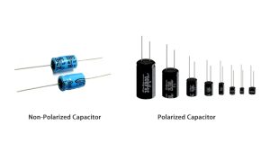
Common examples of passive components include resistors, capacitors, inductors, and transformers.

They are essential for active and passive components for circuit design, handling filtering, timing, load matching, and energy storage.

What Is the Difference Between Active and Passive Components? Comparison Table

Knowing the key differences between these components ensures you select the right parts for your project. Below is a detailed comparison of active vs passive components.

FeatureActive ComponentsPassive ComponentsCommon Use Case
Power RequirementNeeds external power to operateNo external power requiredAll electronic circuits
Core FunctionAmplify, switch, or control electrical signalsStore, dissipate, or transfer energySignal management and power regulation
ExamplesTransistors, ICs, diodes, LEDs, relaysResistors, capacitors, inductors, transformersPCB design and circuit assembly
Energy RoleSupplies energy to the circuitUses or reserves energy from the circuitPower systems and signal processing

What Are the Advantages and Disadvantages of Active Components?

Understanding the advantages of active components and their limitations helps you make informed design decisions.

Advantages: High performance, signal amplification, precise control over circuit behavior, and ability to switch signals quickly.

Disadvantages: Higher cost compared to passive components, requires external power, and adds complexity to PCB design.

What Are the Advantages and Disadvantages of Passive Components?

The advantages of passive components make them indispensable for reliable, cost-effective circuits.

Advantages: Low cost, simple design, high reliability, no external power needed, and long service life.

Disadvantages: No signal amplification capability, limited function, and fixed electrical parameters that cannot be adjusted.

How to Choose Between Active and Passive Components?

Selecting between active and passive components depends on your circuit’s specific needs.

Use active components for amplification, switching, or signal control—ideal for circuits that need to boost or modify signals.

Use passive components for filtering, timing, load matching, or energy storage—critical for stabilizing circuits and managing power flow.
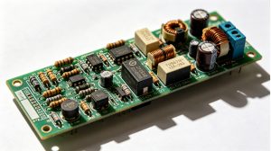
Active and Passive Components in PCB Design (Top 4 Industries)

Consumer Electronics

Smartphones, tablets, and wearables rely on active and passive components in consumer electronics.
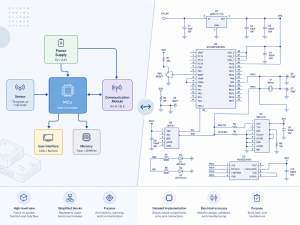
ICs (active) and capacitors (passive) are used to ensure small size, low power consumption, and stable performance.

Automotive Electronics

EV controllers, infotainment systems, and safety modules use active and passive components in automotive electronics.

Transistors (active) and power resistors (passive) meet high reliability and temperature resistance standards for vehicle environments.

Industrial Control & Automation

PLCs (Programmable Logic Controllers) and factory automation systems use active and passive components in industrial electronics.

Relays (active) and inductors (passive) provide signal isolation and stability in harsh factory conditions.

Medical Electronics

Patient monitors, diagnostic devices, and medical implants use active and passive components in medical devices.

Op-amps (active) and precision passive components comply with strict safety and accuracy regulations for medical applications.

How to Identify Active and Passive Components?

Identifying active and passive components is simple with these key indicators.

Active components: Require a power pin or connection (e.g., ICs with VCC pins, transistors with base/emitter pins).

Passive components: No power connection needed (e.g., resistors with two leads, capacitors with two terminals).

Common Failures of Active & Passive Components & Fixes

Even high-quality active and passive components can fail—here’s how to troubleshoot and fix common issues.

Active components: Overheating or voltage damage → Use proper cooling solutions and voltage protection circuits.

Passive components: Parameter drift or short circuits → Select high-quality, rated parts from reliable suppliers.

How Do Active & Passive Components Affect PCB Quality & Supply Chain?

The quality of active and passive components directly impacts PCB performance and supply chain stability.

Quality: Choose certified components to ensure long-term reliability and compliance with industry standards.

Supply chain: Select widely available parts to avoid delays—EBest ensures a stable supply chain for electronic components.

Latest Trends for Active and Passive Components (2026)

The types of active and passive components with examples are evolving to meet industry demands in 2026.

Miniaturization: Smaller component packages for compact PCBs in consumer and medical devices.

High reliability: Automotive and medical grade components with enhanced durability and performance.

Sustainability: Low-power active components and eco-friendly passive components to reduce energy consumption.

FAQ: Frequently Asked Questions About Active and Passive Components

Is a transistor active or passive component?

A transistor is an active component. It requires external power to amplify or switch electrical signals, which is a key characteristic of active components.

Is a resistor active or passive component?

A resistor is a passive component. It dissipates energy as heat and does not require external power to operate, fitting the definition of passive components.

Is a capacitor active or passive?

A capacitor is a passive component. It stores electrical energy and releases it as needed, without requiring external power to function.

Do active components need power?

Yes, active components need external power. They cannot amplify or control signals without a power source, unlike passive components.

Do passive components need a power supply?

No, passive components do not need a power supply. They operate using the energy available in the circuit, such as storing or dissipating energy from active components.

Why are active and passive components important?

Active and passive components are important because they work together to create functional electronic circuits. Active components provide control and amplification, while passive components stabilize and support signal flow.

Active vs passive components which is better?

Neither is “better”—they serve different purposes. Active components are essential for signal control/amplification, while passive components are critical for stability and energy management. Both are required for most circuits.

Summary: Master Active and Passive Components for Better PCBs

active and passive components form the foundation of all electronic circuits. The function of active and passive components works in harmony to ensure circuits perform reliably, efficiently, and cost-effectively.

Correct selection of active and passive components improves PCB quality, reduces failures, and ensures your device meets industry standards.

EBest provides high quality PCB with active and passive components and reliable active and passive components for PCB manufacturing. We specialize in PCB manufacturing with active and passive components and custom PCB using active and passive components, with a stable supply chain and on-time delivery. If you need high-quality components and PCB solutions, place your order with us. Email us at sales@bestpcbs.com for inquiries and quotes.

You may also like

ECU Board Explained: Cleaning, Testing, and Troubleshooting

March 17th, 2026

Are you struggling with ECU board issues like unclear diagnostics, difficult cleaning, or confusing reflashing? This guide provides clear, practical guidance for working with an ECU Board. It offers step-by-step instructions for cleaning, testing, diagnosis, reflashing, and more, all designed to ensure reliable operation and simplify maintenance. Just actionable tips to streamline processes and maintain optimal performance in automotive electronic systems.

ECU Board, https://www.bestpcbs.com/blog/2026/03/ecu-board/

What is an ECU Board?

An ECU board (Electronic Control Unit Board) is a printed circuit board that serves as the central control unit for a vehicle’s electronic systems. It integrates car-grade microcontrollers, memory chips, power management circuits, and input/output interfaces to process real-time data from vehicle sensors, such as engine speed, temperature, and air flow and regulate critical components like fuel injectors and ignition systems. These components work together to enable precise control, including fuel injection timing and ignition advance, ensuring optimal engine performance. While designs vary by vehicle make and model to match specific performance needs, all ECU boards share the core goal of optimizing reliability, fuel efficiency, and overall vehicle functionality.

What Are Types of ECU Board Car?

  • Powertrain ECUs: Control engine (ECU/ECM), transmission (TCU/TCM), hybrid/electric motor (HCU/Motor ECU), and turbocharger systems.
  • Chassis & Safety ECUs: Manage ABS, electronic stability control (ESC), airbags, and tire pressure monitoring.
  • Body & Comfort ECUs: Regulate HVAC, power windows, seats, lighting, and keyless entry.
  • Infotainment & ADAS ECUs: Handle navigation, audio, connectivity (e.g., Bluetooth, GPS), and advanced driver-assistance features (e.g., adaptive cruise control, lane detection).
  • Energy Management ECUs: Oversee battery systems (BMS) in EVs/hybrids, charging processes, and regenerative braking.
What Are Types of ECU Board Car, https://www.bestpcbs.com/blog/2026/03/ecu-board/

What Does ECU Do?

  • Performance Optimization: Adjusts air-fuel ratios, ignition timing, and fuel injection for peak efficiency and power output.
  • Emissions Control: Reduces harmful exhaust emissions via catalytic converter coordination and real-time adjustments.
  • Safety & Reliability: Ensures stable braking (via ABS), airbag deployment, and fault detection (through OBD-II diagnostics).
  • System Integration: Communicates with other ECUs via protocols like CAN, LIN, or Ethernet to synchronize vehicle subsystems (e.g., engine-transmission coordination).
  • Adaptive Capabilities: Uses machine learning/AI in modern ADAS to process sensor data (cameras, radar) for autonomous decisions (e.g., emergency braking, lane-keeping).
  • Diagnostic Support: Triggers warning lights and stores error codes for troubleshooting, enabling quick repairs via diagnostic tools.

How to Clean ECU Board?

Cleaning an ECU board is critical to prevent short circuits and signal interference, issues that cause 30% of ECU malfunctions. Even small debris (as small as 0.1mm) or oil residue can disrupt component connections. Below are step-by-step instructions with precise data for safe, effective cleaning:

Step 1: Power Off and Disassemble

Disconnect the board from the vehicle’s power supply and remove it from its housing. Wait 4-6 minutes (standard for 12V automotive ECUs) to fully discharge capacitors, this prevents electrical arcing that can damage 80% of sensitive microcontrollers on the board. Label connectors before removal to avoid misalignment during reassembly.

Step 2: Choose the Right Cleaner

Optimize for 90-99% isopropyl alcohol (70-80% concentrations leave 5-10% moisture residue, increasing corrosion risk) or a dedicated electronic circuit cleaner (meets IPC-J-STD-001 standards). Avoid water, bleach, or ammonia-based cleaners—they corrode solder joints and reduce component lifespan by up to 50%.

Step 3: Clean Gently

Use a soft-bristle brush (10-15mm bristle length) or compressed air set to 4-6 bar (3-5 bar is too low for stubborn dust; over 6 bar damages surface-mounted components) to remove loose debris. Wipe connectors and component pins with a lint-free cloth or cotton swab dipped in cleaner, spend 10-15 seconds per connector to remove oil residue that causes 40% of connection failures.

Step 4: Dry Thoroughly

Air-dry the board for 20-30 minutes in a well-ventilated area (15 minutes is insufficient for alcohol evaporation in humid environments). For faster drying, use low-temperature air (40-50°C; above 60°C warps PCB traces) with an airflow speed of 1.0-1.5 m/min. Verify no moisture remains with a multimeter (resistance reading ≥1MΩ between power and ground pins) before reassembly.

How to Get Gel off ECU Board?

Below are methods about how to get gel off ECU board:

1. Mechanical Scraping with Non-Conductive Tools: Use a plastic or soft-metal scraper (e.g., nylon spatula, bamboo stick) to gently pry off dried gel. Start from edges and work inward to avoid scratching circuits or components. Safety Tip: Wear anti-static gloves to prevent electrostatic discharge (ESD) damage.

    2. Solvent-Based Dissolution: Apply isopropyl alcohol (≥90% concentration), acetone, or specialized electronic cleaning solvents (e.g., MG Chemicals 824-DW) to the gel using a cotton swab or soft brush. Let it soak for 5–10 minutes to soften the gel, then wipe gently with a microfiber cloth. Critical Note: Test solvents on a small, inconspicuous area first to check for material compatibility (e.g., avoid acetone on acrylic-coated boards).

    3. Controlled Heat Application: Use a heat gun set to 120–150°F (49–66°C) or a hairdryer on low heat to warm the gel. Move the tool continuously to avoid localized overheating. Once softened, use tweezers or a soft brush to remove the gel. Warning: Exceeding 180°F (82°C) may damage solder joints or plastic components.

    4. Ultrasonic Cleaning for Delicate Boards: Submerge the ECU board in an ultrasonic cleaner filled with distilled water or a mild solvent (e.g., deionized water + 5% isopropyl alcohol). Set the machine to 30–40kHz frequency for 3–5 minutes. Key Benefit: Ultrasonic waves dislodge gel without physical contact. Precaution: Remove batteries or sensitive components first to prevent water damage.

    5. Adhesive Remover Gels for Stubborn Residue: Apply a commercial adhesive remover gel (e.g., Goo Gone, De-Solv-It) to the affected area. Let it sit for 15–20 minutes, then wipe with a lint-free cloth. Advantage: These gels are designed to break down sticky residues without harsh chemicals. Follow-Up: Clean the area thoroughly with isopropyl alcohol to remove any remover residue.

    6. Freeze-and-Crack Method (For Non-Sensitive Components): Place the ECU board in a sealed plastic bag and freeze it for 2–3 hours. Remove and immediately tap the gel area gently with a soft hammer or the back of a screwdriver. The cold temperature makes the gel brittle, allowing it to crack and flake off. Limitation: Not recommended for boards with delicate surface-mount components.

    7. Professional Rework Services: For high-value or warranty-protected ECU boards, consult a certified electronics repair service. Professionals use precision tools (e.g., rework stations, vacuum pens) and non-corrosive flux removers to safely extract gel without damaging circuits. Cost-Benefit: Minimizes risk of accidental damage and preserves warranty validity.

      How to Identify Honda ECU Board?

      Identifying a Honda ECU board is critical for accurate replacement and maintenance. Below are clear, actionable methods to identify it easily:

      • Check the Part Number: Every Honda ECU Board has a unique part number printed on the board surface or its housing. A common example is 37820-PNA-003. Always cross-verify this number with Honda’s official part database to confirm compatibility with the vehicle’s make and model. This step avoids incorrect replacements that lead to functionality issues.
      • Look for Branding: Most Honda ECU Boards feature the Honda logo or Honda Motor Co. printing on the board or housing. They often include branding from Honda’s trusted partners such as Denso. This branding is typically clear and visible, even after years of use, making it a quick identification marker.
      • Examine Connector Layout: Honda uses standardized connectors for its ECU Boards. Civic models usually have 32 pin connectors while Accord models commonly use 48 pin connectors. Match the connector count and shape to the vehicle’s specifications to ensure the ECU Board is compatible. This is especially useful for older Honda models where part numbers may be worn or unreadable.
      • Verify ECU Labeling: Many Honda ECU Boards have additional labeling indicating the PGM Fi system which is Honda’s proprietary electronic fuel injection system. This labeling confirms the board is designed for Honda’s specific engine management needs, further ensuring accuracy in identification.
      How to Identify Honda ECU Board, https://www.bestpcbs.com/blog/2026/03/ecu-board/

        How to Reflash ECU Circuit Board?

        Reflashing an ECU board updates its firmware to fix bugs, improve performance, or adapt to modified components, critical for avoiding costly replacements. Below are actionable, detail-rich steps to ensure successful reflashing without damaging the board:

        Step 1: Gather Tools

        Use a reflashing tool compatible with the vehicle’s make and model, such as Honda HDS for Honda vehicles or tools supporting SAE J2534 standards for broader use. Ensure the laptop has the correct firmware file that matches the ECU part number to avoid corruption. Prepare a stable 12V external power supply. Unstable power causes 40% of reflashing failures, so avoid relying solely on the vehicle’s battery.

        Step 2: Connect the Tool

        Connect the reflashing tool to the vehicle’s OBD-II port. For problematic connections, remove the ECU and connect the tool directly to the board. Keep the vehicle’s engine off, engage the parking brake and turn off all accessories like lights and radio to reduce power draw. Confirm the power supply reads 12.4-12.7V for stable operation.

        Step 3: Backup Firmware

        Backup the ECU’s current firmware before proceeding. This step is essential to restore the board if reflashing fails or corrupts data. Save the backup file to the laptop and a secondary storage device. Label it with the vehicle’s VIN and ECU part number for easy retrieval. Verify the backup file size matches the ECU’s firmware size for added security.

        Step 4: Flash New Firmware

        Load the correct firmware file into the reflashing tool and follow on-screen prompts without skipping any steps. Keep the tool and laptop connected and powered on throughout the 5-10 minute process. Interruptions such as power loss or disconnection will brick the ECU and render it unusable. Do not adjust tool settings or run other software on the laptop during this time to avoid signal interference.

        Step 5: Verify and Test

        Disconnect the reflashing tool, turn off the vehicle’s ignition and wait 5 seconds before restarting. Use a diagnostic scanner to check for error codes. Clear any minor codes and retest. Verify key functions including engine start, sensor readings and actuator response to confirm the firmware update was successful. Reload the backup firmware and retry if the ECU fails to communicate.

        How to Test ECU Board Car?

        Testing a car ECU board ensures functionality before installation, reducing costly downtime. Use these methods:

        • Visual Inspection: Check for cracked solder joints, bulging capacitors, burnt components, or corrosion, common causes of ECU Board failure.
        • Voltage Testing: Use a multimeter to measure the ECU Board’s 12V power supply and ground connections. Stable voltage prevents erratic performance.
        • Signal Testing: Use an oscilloscope to check sensor input and actuator output signals. Ensure they fall within the manufacturer’s specified range.
        • Diagnostic Scanner Test: Connect an OBD-II scanner to read error codes. Clear codes, then test the vehicle to identify hidden ECU Board issues.
        How to Test ECU Board Car, https://www.bestpcbs.com/blog/2026/03/ecu-board/

        How to Diagnose an ECU Board?

        Here are step-by-step guide for effective diagnosis:

        Initial Visual Inspection

        • Check for physical damage (burnt components, corroded connectors, loose wires).
        • Verify all connections (OBD-II port, wiring harnesses) are secure and free of debris.
        • Look for water damage or moisture ingress, common in flood-affected vehicles.

        Diagnostic Tool Scanning

        • Use a manufacturer-specific scanner (e.g., Toyota Techstream, BMW ISTA) or universal tool (SAE J2534) to read fault codes.
        • Prioritize active codes (current issues) over historical codes (past problems).
        • Clear codes after recording to distinguish intermittent vs. persistent issues.

        Power & Ground Checks

        • Measure voltage at ECU power pins (should be 12–14V with ignition on).
        • Test ground connections for continuity (resistance <0.5Ω).
        • Poor grounding causes 30% of ECU failures, verify with multimeter.

        Sensor & Actuator Testing

        • Use a multimeter to check sensor inputs (e.g., MAP, TPS, oxygen sensors) for correct voltage/signals.
        • Test actuators (fuel injectors, ignition coils) for proper operation via scan tool activation.
        • Compare live data against manufacturer specifications to identify deviations.

        Software & Firmware Verification

        • Ensure the ECU software version matches the vehicle’s VIN and model year.
        • Update firmware only if a manufacturer-approved patch exists for known bugs.
        • Avoid unofficial firmware, risk of bricking the ECU.

        Bench Testing (Advanced)

        • For suspected hardware faults, remove the ECU and test on a bench with a simulator.
        • Check components (capacitors, resistors) for proper values using a component tester.
        • Replace faulty components or send to a specialist for micro-soldering repairs.

        How to Replace an ECU Board?

        Replacing an ECU Board requires precision to ensure compatibility. Follow these steps:

        Step 1: Select the Correct Replacement

        Choose an ECU board that matches the vehicle’s make model and year. Ensure it meets original equipment quality standards to avoid compatibility issues.

        Step 2: Disconnect the Old ECU

        Turn off the vehicle power disconnect the battery and remove the old ECU Board. Note the position of each connector to prevent misconnection during reinstallation.

        Step 3: Install the New ECU

        Align the new ECU Board with its housing connect all connectors securely and fasten the board properly to prevent damage from vehicle vibration.

        Step 4: Reconnect Power and Program

        Reconnect the battery turn on the vehicle and program the new ECU Board using the vehicle’s VIN with a diagnostic scanner. Proper programming ensures the ECU works with the vehicle’s systems.

        Step 5: Test the Vehicle

        Test the vehicle including engine start acceleration and other key functions. Use a diagnostic scanner to check for error codes and confirm successful replacement.

        Is ECU Board Repair Better Than Replacement?

        When your ECU Board malfunctions, choosing between repair and replacement is a decision that directly impacts your time, cost and vehicle reliability. As someone who works with these components regularly, you want a solution that is cost-effective, efficient and minimizes downtime.

        Repair is often the best choice for minor ECU circuit board issues. If the problem is loose solder, damaged connectors or faulty capacitors, repairing these specific parts is far more affordable than replacing the entire board. This is especially true if you have a rare or expensive ECU boards that is hard to source. Repairing also saves time on waiting for a new board to be delivered, getting your vehicle back in operation faster without compromising on functionality.

        Replacement becomes necessary when the ECU circuit board has severe damage that cannot be fixed. If the microcontrollers are burnt, the PCB traces are cracked or the firmware is irreparably corrupted, repairing the board is not feasible. You should also consider replacement if the cost of repairs exceeds 70% of the price of a new board. A new ECU board ensures reliability and avoids the risk of repeated breakdowns that come with patching a severely damaged unit, which ultimately saves you time and money in the long run.

        Would ECU Affects Cluster Board?

        Yes, the ECU can affect the cluster board. The ECU shares critical data like speed, RPM, fuel level, and warnings with the cluster via vehicle networks such as CAN bus. It also controls cluster functions, including warning light activation and gauge display behavior.

        A faulty ECU can disrupt this process. Common effects include erratic speedometer readings, frozen fuel gauges, false warning lights, or dimmed display screens. These issues compromise driver awareness and vehicle safety.

        To diagnose, scan for ECU fault codes or communication errors using a diagnostic tool. Inspect CAN bus wiring for damage or corrosion. Test the cluster with a known-good unit to confirm if the ECU is the root cause. This streamlined approach ensures quick identification of ECU-related cluster problems, enabling efficient repairs and reliable vehicle operation.

        Conclusion

        By following the practical guidance outlined in this blog you can effectively maintain, troubleshoot and care for your vehicle’s central control unit ensuring consistent performance and avoiding costly downtime. Prioritizing quality components, regular maintenance and timely issue resolution will keep your vehicle’s electronic systems running smoothly for years to come.

        You may also like

        A Guide to PCB Prototyping in Vietnam: Quality, Costs & Lead Time

        March 17th, 2026

        Are you looking for a reliable, cost-effective option for high-quality circuit board samples that aligns with your project timeline and budget? If so, PCB prototyping in Vietnam may be the perfect solution for your needs. Vietnam has built a mature manufacturing ecosystem paired with advanced assembly capabilities, making it a trusted choice for global clients who need rapid prototyping services. It combines competitive pricing, strict quality control and flexible lead times to meet the unique demands of projects in the medical, aerospace and industrial equipment sectors..

        PCB Prototyping in Vietnam, https://www.bestpcbs.com/blog/2026/03/pcb-prototyping-in-vietnam/

        Are You Facing these Pain Points of PCB Prototyping in Vietnam?

        • Do you struggle with inconsistent prototype quality that leads to repeated rework and project delays?
        • Is the promised lead time not met, disrupting your production schedule?
        • Are hidden fees inflating your project costs, especially when combining assembly and prototyping services?
        • Do communication gaps with manufacturing providers result in prototypes that don’t match your design specs?
        • Is it challenging to find prototyping services that meet strict medical or aerospace quality standards?
        • Do rigid minimum order quantities force you to overorder, wasting resources and increasing costs?

        Our Targeted Solutions to These Pain Points

        • Adhere to ISO 9001 and IPC-A-600 quality standards, achieving a 99.8% prototype pass rate to eliminate costly rework. Advanced AOI and X-Ray testing for every batch ensures zero defects, critical for medical device prototypes that demand absolute reliability.
        • Guarantee on-time delivery with transparent scheduling and real-time order tracking. We prioritize urgent projects, even complex 16-layer HDI prototypes for aerospace use, so your production timeline stays on track without delays.
        • Offer all-inclusive pricing with no hidden fees: detailed upfront quotes cover assembly, materials, and testing. This lets you lock in budgets upfront, avoiding unexpected costs that inflate industrial equipment prototyping expenses.
        • Assign dedicated English-speaking project managers available 24/7 to clarify requirements and resolve issues quickly, ensuring your prototypes match design specs perfectly, first time around.
        • Hold ISO 13485 and AS9100 certifications, meeting strict medical and aerospace industry standards. This compliance eliminates regulatory risks for surgical generator and aerospace control panel prototypes.
        • Provide flexible MOQs starting at 1 piece, so you only order what you need, no excess prototypes, no wasted resources, and lower upfront costs for small-scale testing or R&D.

        Why Choose EBest for PCB Prototyping in Vietnam?

        Here are reasons why choose EBest for PCB prototyping in Vietnam:

        • We have nearly 20 years of experience in PCB prototyping and manufacturing in Vietnam, serving 1200+ global clients across medical, aerospace, and industrial sectors with a 99.6% client retention rate, ensuring you partner with a reliable, seasoned provider.
        • Our advanced production equipment includes 8 sets of HDI production lines, supporting up to 24-layer HDI boards and flexible PCB prototyping with a minimum line width/space of 0.1mm, perfectly accommodating complex designs for aerospace communication modules and high-precision medical devices.
        • We strictly comply with ISO 9001, ISO 13485, AS9100 international quality standards, with 100% of medical prototypes meeting FDA and CE regulatory requirements and 99.9% of aerospace prototypes passing AS9100 compliance audits, eliminating your regulatory risks.
        • We offer rapid lead times, with 24-72 hours for standard 1-4 layer prototypes and 5-7 days for complex 9-16 layer HDI boards, and we maintain a 99.7% on-time delivery rate, accelerating your project timeline and avoiding costly production delays.
        • Our one-stop service integrates PCB prototyping, assembly, and post-production testing, reducing your supply chain links by 60% and cutting coordination time by 40%, simplifying your workflow and lowering overall project management costs.
        • We have delivered 10,800+ medical PCB prototypes for surgical generators, achieving zero defects and 100% FDA compliance, and 3,200+ aerospace control panel prototypes that all meet AS9100 standards, proving our ability to deliver high-quality products for critical applications.
        • Our eco-friendly production processes meet Vietnam environmental regulations and RoHS standards, with 95% of production waste recycled and no hazardous substances used, ensuring your prototypes are compliant with global environmental requirements and avoiding export restrictions.
        • We provide flexible customization options, including 12+ special materials such as Rogers and Teflon, and 5 surface treatments including ENIG and HASL, with a 48-hour response time for custom requests, adapting perfectly to your unique project needs.
        • Our transparent order management system updates order status every 4 hours, allowing you to track every stage of prototyping in real time, with 24/7 access to production logs and test reports, eliminating uncertainty and improving project visibility.
        Why Choose EBest for PCB Prototyping in Vietnam, https://www.bestpcbs.com/blog/2026/03/pcb-prototyping-in-vietnam/

        Top 10 PCB Prototyping Factories in Vietnam in 2026

        Factory NameAdvantagesProcess CapabilitiesLead Time
        EBest20+ years of experience, medical/aerospace certifications, one-stop service, 99.8% pass rate1-24 layers, HDI, flexible PCB, rigid-flex, surface treatments (ENIG, HASL), AOI/X-Ray testing24-72 hours (standard), 5-7 days (complex), 24-hour urgent service
        Meiko Electronics VietnamJapanese-owned, high-precision HDI, Apple supplier, advanced production lines1-16 layers, HDI (16-layer), FPC, PTH/B/U boards, 99.2% yield rate3-5 days (standard), 7-10 days (complex)
        Hongban Technology VietnamChinese-invested, large-scale production, eco-friendly processes, competitive pricing1-12 layers, rigid PCB, surface mount technology, 600,000ã¡ annual capacity4-6 days (standard), 8-10 days (complex)
        Tripod Vietnam (Chauduc) ElectronicTaiwanese-owned, server/NB board expertise, large capacity, strict quality control1-18 layers, HDI, server boards, 372,000ã¡ annual capacity5-7 days (standard), 10-12 days (complex)
        Vietnam FICT Co., LtdMature production lines, cost-effective, quick response, reliable delivery1-10 layers, rigid PCB, through-hole technology, basic surface treatments3-7 days (standard), 8-10 days (complex)
        Vina PCB ManufacturingLocal Vietnamese factory, small-batch expertise, flexible MOQ, personalized service1-8 layers, rigid PCB, simple HDI, ENIG/HASL surface treatments4-8 days (standard), 9-11 days (complex)
        Hanoi PCB SolutionsHanoi-based, quick turnaround, industrial PCB focus, competitive pricing1-10 layers, rigid PCB, industrial-grade materials, basic testing3-6 days (standard), 7-9 days (complex)
        Saigon Electronics PCBHo Chi Minh-based, large-scale capacity, export-oriented, RoHS compliant1-12 layers, rigid/flexible PCB, Vietnam PCB assembly, mass prototyping5-7 days (standard), 10-13 days (complex)
        Danang PCB TechCentral Vietnam location, specialized in medical PCB, ISO 13485 certified1-14 layers, medical-grade PCB, HDI, strict sterility control6-8 days (standard), 10-12 days (complex)
        Hai Phong PCB WorksNorthern Vietnam base, automotive PCB specialization, IATF 16949 certified, 24/7 production1-10 layers, automotive-grade PCB, high-temperature materials, in-circuit testing4-6 days (standard), 8-11 days (complex)

        What’s the Minimum Order for PCB Prototypes in Vietnam Factories?

        The minimum order quantity (MOQ) for PCB prototyping in Vietnam varies by factory, process complexity, and board type. There is no universal MOQ, but most factories offer flexible options to meet different project needs.

        For standard rigid PCB prototypes (1-4 layers, simple design), MOQs start at 1 piece. This is ideal for small-scale testing or single-unit validation, common in medical device R&D (e.g., portable surgical tool prototypes).

        For complex prototypes (8+ layers, HDI, flexible PCB, or special materials like Rogers), MOQs typically range from 5-10 pieces. These require more advanced production processes, so factories set a minimum to cover material and setup costs, such as aerospace control panel prototypes.

        Some factories offer MOQ waivers for urgent projects or long-term clients, but this may result in slightly higher unit costs. Always confirm MOQ with your PCB manufacturing in Vietnam provider before placing an order to avoid unexpected costs.

        What Quality Certifications Should PCB Manufacturing in Vietnam Have?

        Below are quality certifications should PCB manufacturing companies in Vietnam have:

        • ISO 9001: The basic quality management system certification, required for all reputable PCB manufacturing in Vietnam providers. It ensures consistent production processes and product quality.
        • ISO 13485: Mandatory for PCB prototyping in Vietnam serving the medical industry. It covers quality management for medical devices, ensuring prototypes meet FDA and CE medical standards (e.g., surgical generator PCBs).
        • AS9100D: Required for aerospace PCB prototyping in Vietnam. It aligns with aerospace industry standards, ensuring prototypes meet strict reliability and performance requirements for aircraft components.
        • IPC-A-600: A critical standard for PCB quality, specifying acceptability criteria for printed circuit boards. All PCB prototyping in Vietnam services should adhere to this to ensure consistent board quality.
        • QC080000: A hazardous substance process management certification, ensuring PCB manufacturing in Vietnam complies with RoHS, WEEE, and Vietnam environmental regulations, avoiding harmful materials.
        • UL Certification: Optional but recommended for PCB prototypes used in electrical equipment, ensuring compliance with safety standards for global markets.

        What Is Quality Control Process of Vietnam PCB Prototyping Services?

        Quality Control Process of Vietnam PCB Prototyping Services:

        • Pre-production QC: Conduct Incoming Quality Control (IQC) on raw materials such as copper, substrate and solder mask. Verify material certificates and perform sample tests to ensure all materials meet project requirements, including medical-grade FR-4 substrate for medical prototypes.
        • In-production QC: Monitor every production step closely, with drilling accuracy controlled to ±0.05mm and copper plating thickness no less than 25μm. Use Automatic Optical Inspection (AOI) to identify surface defects like short circuits and missing pads in real time.
        • Post-production QC: Perform X-Ray testing to detect hidden defects, such as issues with BGA solder joints in aerospace prototypes. Conduct electrical tests for continuity and insulation resistance, along with visual inspections per IPC-A-600 standards. Add sterility and biocompatibility tests for medical prototypes.
        • Final validation: Compile a detailed QC report with all test results to ensure full traceability for each prototype batch, supporting medical and aerospace clients in meeting relevant regulatory requirements.
        What Is Quality Control Process of Vietnam PCB Prototyping Services, https://www.bestpcbs.com/blog/2026/03/pcb-prototyping-in-vietnam/

        What Are Production Capabilities of PCB Prototyping in Vietnam?

        PCB prototyping in Vietnam has advanced production capabilities to meet diverse industry needs, with most factories offering comprehensive services for medical, aerospace, and industrial equipment.

        • Board Layers: 1-24 layers, including HDI (High-Density Interconnect) boards up to 16 layers (used in aerospace communication modules) and rigid-flex boards for portable medical devices.
        • Board Size: 0.8cm × 0.8cm to 100cm × 100cm, supporting both small precision prototypes (e.g., medical sensors) and large industrial PCB prototypes (e.g., industrial control panels).
        • Materials: FR-4 (standard), Rogers (high-frequency, aerospace), Teflon (high-temperature), aluminum substrate (heat-dissipating, industrial equipment), and medical-grade materials (biocompatible, non-toxic).
        • Surface Treatments: ENIG (Electroless Nickel Immersion Gold), HASL (Hot Air Solder Leveling), OSP (Organic Solderability Preservative), and immersion silver, suitable for different soldering and reliability requirements.
        • Special Processes: Blind/buried vias, microvias (HDI), solder mask printing, silkscreen printing, and conformal coating (for harsh industrial environments). Annual capacities range from 540,000ã¡ (FPC) to 2.16 millionã¡ (PTH boards) for top factories.
        What Are Production Capabilities of PCB Prototyping in Vietnam, https://www.bestpcbs.com/blog/2026/03/pcb-prototyping-in-vietnam/

        What Is the Typical Lead Time of PCB Prototyping in Vietnam?

        PCB Prototype TypeStandard Lead TimeUrgent Lead Time (Additional Fee)
        1-4 Layers (Standard Rigid PCB)24-72 Hours12-24 Hours (+50%)
        5-8 Layers (Mid-Range Rigid PCB)4-5 Days2-3 Days (+30%)
        9-16 Layers (HDI/Complex PCB)5-7 Days3-4 Days (+40%)
        Flexible/Rigid-Flex PCB7-10 Days5-6 Days (+35%)
        Special Materials (Rogers/Teflon)8-12 Days6-7 Days (+45%)
        PCB + Vietnam PCB Assembly10-14 Days7-8 Days (+30%)

        How Much Does PCB Prototyping in Vietnam Cost?

        The cost of PCB prototyping in Vietnam depends on board layers, size, materials, surface treatment, and quantity. Below are accurate price ranges for 2026, excluding Vietnam PCB assembly:

        • 2 Layers (Standard FR-4, 10×10cm, 10 pieces): $20-$50.
        • 4 Layers (Standard FR-4, 10×10cm, 10 pieces): $50-$120.
        • 8 Layers (Standard FR-4, 10×10cm, 10 pieces): $120-$250.
        • 16 Layers (HDI, FR-4, 10×10cm, 10 pieces): $250-$500.
        • Flexible PCB (2-4 layers, 5×5cm, 10 pieces): $80-$180.
        • Special Materials (Rogers/Teflon, 1-4 layers, 10×10cm, 10 pieces): $150-$350.
        • Surface Treatment Add-Ons: ENIG (+$30-$80 per batch), HASL (+$10-$30 per batch), OSP (no additional cost).
        • Urgent Service: +30%-50% of the total prototyping cost.

        For Vietnam PCB assembly, add $0.01-$0.05 per solder joint for standard components, or $0.05-$0.10 per joint for precision components (e.g., 01005 size for medical devices).

        FAQs About PCB Prototyping Services in Vietnam

        Q1: Can PCB prototyping services in Vietnam handle custom material requests for high-frequency or high-temperature aerospace prototypes?
        A1: Yes, most reputable PCB prototyping services in Vietnam can accommodate custom material requests for aerospace and other high-demand applications. They offer a range of specialized materials, including Rogers for high-frequency needs and Teflon for high-temperature resistance, which are essential for aerospace communication modules. Top factories maintain partnerships with global material suppliers, ensuring timely access to these specialized materials, and can provide material certificates to verify compliance with aerospace industry standards.

        Q2: If my PCB prototype fails quality testing, what is the process for rework or replacement with Vietnam prototyping services?
        A2: Reputable PCB prototyping services in Vietnam have a clear rework and replacement policy to protect client interests. If a prototype fails quality testing (e.g., electrical continuity issues or surface defects), the factory will first conduct a detailed root cause analysis within 24 hours. For defects caused by production errors, they will provide free rework or replacement, with the rework lead time typically 20%-30% shorter than the original prototyping time. For medical and aerospace prototypes, they also offer additional testing after rework to ensure compliance with all specs.

        Q3: Do PCB prototyping services in Vietnam offer component sourcing support for prototypes that require assembly?
        A3: Yes, most PCB prototyping services in Vietnam provide component sourcing support as part of their one-stop service. They source components from trusted global suppliers such as TI and ADI, ensuring genuine parts that meet project specifications. For hard-to-find or specialized components (e.g., precision parts for medical device prototypes), they have a dedicated sourcing team that can locate components within 48 hours, and they provide component quality verification before assembly to avoid compatibility issues.

        Q4: How do PCB prototyping services in Vietnam ensure design confidentiality for my proprietary PCB prototypes?
        A4: Confidentiality is a top priority for PCB prototyping services in Vietnam, especially for clients with proprietary designs. All reputable factories require non-disclosure agreements (NDAs) to protect client intellectual property. They also implement strict internal data security measures, including encrypted design file storage, restricted access to design data, and secure disposal of unused prototype materials and design documents. Additionally, they do not share client design details or prototype samples with third parties without explicit permission.

        Q5: Can PCB prototyping services in Vietnam accommodate design modifications after the prototyping process has started?
        A5: Most PCB prototyping services in Vietnam can accommodate design modifications, but the feasibility depends on the stage of production. If modifications are requested before the production of core layers (e.g., drilling or copper plating), the process is straightforward, with minimal additional cost and a short delay of 12-24 hours. If modifications are requested after core production, there may be additional material and labor costs, but the factory will provide a detailed cost and timeline estimate before proceeding. For urgent projects, they prioritize modification requests to minimize delays to the overall project timeline.

        You may also like

        GPS Antenna PCB Manufacturer | Fast Prototyping, Design and Assembly

        March 17th, 2026

        GPS Antenna PCB is a specialized printed circuit structure designed to receive satellite signals and convert them into stable positioning data for devices such as trackers, automotive systems, IoT modules, and industrial equipment. This article explains how GPS antenna PCB design, material selection, frequency planning, assembly control, and testing work together when choosing a reliable manufacturer for fast prototyping, design, and assembly.

        Are you struggling with unstable signal performance, repeated antenna tuning, or unclear supplier capabilities when sourcing a gps antenna pcb manufacturer?

        • The prototype performs well in lab conditions but fails in the final product
        • Antenna matching shifts after PCB fabrication
        • GPS signal becomes weak after enclosure integration
        • Supplier lacks RF understanding beyond PCB fabrication
        • Quotation and engineering response are slow

        These issues often come from a disconnect between design, material selection, and manufacturing execution.

        • Align antenna design with real product structure from the beginning
        • Select materials based on RF behavior, not just cost
        • Control PCB fabrication tolerances for RF consistency
        • Integrate layout, assembly, and testing as one process
        • Provide fast engineering feedback and prototyping support

        EBest Circuit (Best Technology) is a professional PCB and PCBA manufacturer with strong experience in RF-related products. We support gps antenna pcb design, gps antenna pcb layout, and full assembly services, helping customers move efficiently from concept to mass production. Ready to move your GPS antenna PCB project forward? Contact our team at sales@bestpcbs.com for fast engineering support and manufacturing solutions.

        GPS Antenna PCB

        What Is a GPS Antenna PCB?

        A GPS antenna PCB is not simply a circuit board carrying a GNSS module. In many modern designs, the antenna itself is implemented directly on the PCB or integrated into it as part of the RF structure.

        From an engineering perspective, a gps antenna on pcb must handle extremely weak satellite signals while operating inside complex electronic environments. This includes interference from processors, power circuits, shielding, and enclosure materials.

        Key structural elements

        • Radiating element (patch or trace)
        • RF feed line
        • Ground plane
        • Matching network
        • Optional LNA (for active designs)
        ElementRole
        AntennaReceives satellite signal
        Feed lineTransfers RF signal
        Ground planeStabilizes performance
        Matching networkEnsures impedance matching
        LNAAmplifies weak signals

        In essence, a GPS antenna PCB behaves more like an RF component than a conventional PCB, which is why manufacturing precision directly impacts performance.

        GPS Antenna PCB

        What Are the Main Types of GPS PCB Antennas? (Patch vs Trace vs Active)

        When selecting a gps pcb antenna, engineers are not just choosing a structure—they are defining how the antenna interacts with the entire system.

        Main antenna types

        1. Patch antenna
          Provides stable performance and is widely used in navigation systems.
        2. PCB trace antenna
          A gps PCB trace antenna is etched directly on the board, reducing cost but increasing sensitivity to layout conditions.
        3. Active antenna
          An active gps antenna pcb includes an amplifier to improve signal strength in weak environments.
        4. Flexible antenna
          A flexible pcb gps antenna allows placement flexibility in compact devices.
        5. GPS + Cellular antenna
          A gsm gps pcb antenna integrates positioning and communication but requires careful isolation.
        TypeAdvantageLimitation
        PatchStable performanceNeeds ground plane
        TraceLow costEasily detuned
        ActiveHigh sensitivityMore complex
        FlexFlexible placementSensitive to structure
        ComboSpace savingRF interference risk

        The choice depends on product size, signal requirements, and integration complexity.

        GPS Antenna PCB

        What Materials Are Used in Flexible PCB GPS Antennas?

        Flexible GPS antennas typically use polyimide substrates, allowing the antenna to be positioned away from interference sources.

        However, material selection is not just about flexibility. It directly affects signal stability, loss, and repeatability.

        Material comparison

        MaterialUse CaseAdvantageLimitation
        FR4Standard designsLow costHigher RF loss
        RF materialsHigh-performance designsStable dielectricHigher cost
        Flex (Polyimide)Compact devicesFlexible placementHarder tuning

        In real-world projects:

        • FR4 is widely used for cost-sensitive designs
        • RF materials are chosen for performance-critical applications
        • Flex is selected when mechanical constraints dominate

        The best material is always determined by system-level requirements, not just electrical specifications.

        How to Design a GPS Patch Antenna PCB?

        A gps patch antenna pcb design begins with frequency selection, ground plane definition, and system constraints.

        Design process

        • Define operating frequency
        • Select antenna structure
        • Estimate dimensions based on wavelength
        • Ensure continuous ground plane
        • Control RF feed impedance
        • Reserve matching network area
        • Validate through testing

        Key layout rules

        • Keep RF area isolated from digital noise
        • Avoid ground discontinuities
        • Minimize feed length
        • Maintain symmetry
        • Allow tuning flexibility

        A well-designed antenna depends more on layout discipline than theoretical complexity.

        What Frequency Bands Do GPS PCB Antennas Operate In? (L1 / L2 / L5)

        GPS antenna PCB design is based on L-band frequencies, but different applications may require different frequency combinations.

        Main frequency bands

        BandFrequencyTypical Use
        L11575.42 MHzStandard GPS
        L21227.60 MHzDual-frequency
        L51176.45 MHzHigh reliability

        In most commercial designs, L1 remains the primary target. However, advanced applications may use multiple bands to improve positioning accuracy.

        For gps glonass pcb antenna or multi-constellation systems, bandwidth requirements increase, making design more complex.

        The key point is that frequency selection defines antenna size, material choice, and matching strategy.

        How to Calculate GPS Antenna Wavelength and Patch Size?

        A fundamental step in antenna design is calculating wavelength.

        GPS Antenna PCB

        For L1 frequency:

        GPS Antenna PCB

        However, real antenna size depends on the effective dielectric constant:

        GPS Antenna PCB

        Practical design steps

        • Calculate free-space wavelength
        • Adjust for substrate properties
        • Determine initial patch size
        • Optimize through testing

        Actual dimensions are influenced by:

        • Substrate thickness
        • Ground plane size
        • Feed position
        • Enclosure effects

        So calculations provide a starting point, but tuning is always required.

        What Are the Challenges in GPS Antenna PCB Assembly?

        Assembly plays a critical role in antenna performance.

        Common challenges

        • Placement misalignment
        • Solder thickness variation
        • Board warpage
        • Shield interference
        • Cable coupling

        For active pcb gps antenna, these issues become more critical due to amplification effects.

        FactorImpact
        PlacementFrequency shift
        SolderImpedance change
        GroundSignal instability
        ShieldingRadiation distortion

        Assembly must be treated as part of RF design, not a separate process.

        Top 10 GPS PCB Antenna Design Factories in China

        Below is a practical reference list of companies active in GPS antenna and RF PCB manufacturing:

        CompanyPositioning
        EBest CircuitPCB + PCBA + RF support
        C&T RF AntennasCustom antenna design
        JC AntennaGNSS antenna specialist
        Tengxiang ElectronicsRF components manufacturer
        Signal PlusGPS antenna supplier
        NHAITCustom FPC antenna
        Keesun TechnologyEmbedded antenna provider
        Chang HongGNSS antenna supplier
        Leheng ElectronicsGPS antenna solutions
        Bynav ecosystemGNSS system providers

        Choosing a supplier should focus on engineering capability, not just production capacity.

        What Are the Applications of GSM GPS PCB Antennas?

        A gsm gps pcb antenna is widely used in connected devices.

        Typical applications

        • Vehicle tracking
        • Fleet management
        • IoT devices
        • Smart meters
        • Security systems
        • Wearables

        These applications require both positioning and communication, making integrated antenna solutions essential. Pls feel free to reach out to our engineering team at sales@bestpcbs.com for fast support and reliable solutions.

        How to Test GPS Antenna PCB Performance? (Gain / Return Loss)

        Testing ensures real-world performance.

        Key parameters

        • Return loss (S11)
        • Gain

        Practical validation steps

        1. Measure return loss
        2. Verify frequency alignment
        3. Test signal reception
        4. Evaluate in final enclosure
        5. Compare multiple samples

        A common mistake is testing only on a bare PCB. Final product testing is essential.

        How to Get GPS PCB Antenna Quotes from EBest Circuit (Best Technology)?

        To get accurate gps pcb antenna quotes, prepare:

        • Gerber files
        • Frequency requirements
        • Material preference
        • Board dimensions
        • Assembly requirements
        • Quantity
        GPS Antenna PCB

        To summarize‌, GPS Antenna PCB is a critical RF structure that determines positioning accuracy and signal reliability in modern electronic devices. This article covered antenna types, materials, design methods, frequency bands, calculations, assembly challenges, and testing processes.

        EBest Circuit (Best Technology) provides complete support from design review to PCB fabrication and PCBA assembly, ensuring faster development and more reliable RF performance. Pls feel free to send your files to sales@bestpcbs.com for fast evaluation and quotation.

        FAQs About GPS Antenna PCBs

        1. What is the most common GPS antenna type?
        Patch antennas are widely used due to stable performance.

        2. Can FR4 be used?
        Yes, but performance may vary compared to RF materials.

        3. Why does performance change after assembly?
        Because enclosure and components affect RF behavior.

        4. What is an active antenna?
        An antenna with an integrated amplifier.

        5. Can GPS and cellular share one PCB?
        Yes, but requires careful RF design.

        You may also like

        5G Antenna PCB Manufacturer | Design, Prototyping & Assembly

        March 17th, 2026

        5G antenna PCB is a printed circuit board engineered to support high-frequency antenna structures, stable RF transmission, and compact wireless integration in modern 5G devices. This article explains what a 5G antenna PCB is, how it is designed, which materials and structures are used, and how to choose a reliable manufacturer for design, prototyping, and assembly.

        Common customer pain points:

        • Simulation results look good, but real testing fails.
        • FR-4 is used to reduce cost, yet signal loss becomes unacceptable.
        • PCB suppliers lack RF design understanding.
        • Prototyping cycles are too slow for fast product iteration.
        • PCB and assembly are handled by different vendors, causing misalignment.

        Corresponding solutions:

        • Co-design antenna layout, stack-up, and matching networks early.
        • Select low-loss materials based on frequency and efficiency targets.
        • Conduct DFM reviews focused on RF-critical structures.
        • Provide rapid prototyping with stable process control.
        • Offer one-stop PCB fabrication and assembly services.

        EBest Circuit (Best Technology) is an engineering-driven PCB and PCBA manufacturer specializing in RF and antenna PCB solutions. With integrated capabilities from design review to assembly, we help customers reduce iteration risk and accelerate product development. For inquiries, please contact sales@bestpcbs.com.

        5G Antenna PCB

        What Is a 5G Antenna PCB?

        A 5G antenna PCB is not simply a circuit board with an antenna pattern. In reality, it is a highly integrated RF platform where antenna geometry, dielectric material, copper structure, and layout all directly influence signal behavior.

        Key characteristics:

        • Integrates antenna directly into PCB structure
        • Supports sub-6 GHz and mmWave frequency bands
        • Requires precise impedance and loss control
        • Often used in MIMO or multi-antenna systems
        • Sensitive to layout, grounding, and surrounding components

        5G communication typically operates across two major frequency domains: sub-6 GHz and mmWave, and each range places very different demands on antenna size, material selection, and layout precision. In practical engineering, sub-6 GHz designs prioritize coverage and stability, while mmWave solutions focus more on bandwidth, beam control, and array integration.

        In essence, a 5g pcb antenna is both a structural and electrical component that defines wireless performance.

        What Are the Types of 5G Antenna PCBs?

        Different applications require different antenna structures, and selecting the right type is critical for performance.

        Common types:

        • Patch antenna PCB
        • PIFA / IFA antenna PCB
        • Slot antenna PCB
        • Dipole / monopole PCB antenna
        • Array antenna PCB
        • Flexible PCB antenna

        Comparison:

        TypeAdvantageApplication
        PatchDirectional gainBase stations
        PIFACompactMobile devices
        SlotFlexible layoutShielded systems
        DipoleSimple designExternal antennas
        ArrayBeamformingmmWave systems
        FlexibleSpace-savingWearables

        Each type must align with enclosure design, ground reference, and frequency band.

        What Materials Are Used in 5G Antenna PCBs?

        Material selection is one of the most critical factors in 5g antenna pcb manufacturing.

        Common materials:

        • FR-4
        • Rogers
        • PTFE-based laminates
        • LCP
        • Hybrid stack-ups

        Material comparison:

        MaterialCostRF PerformanceUsage
        FR-4LowLimitedEntry-level
        RogersMediumHighRF boards
        PTFEHighExcellentMicrowave
        LCPMediumStrongCompact antennas
        HybridMediumBalancedCost-performance

        In high-frequency PCB design, material selection is not just about dielectric constant, but also about loss tangent stability, copper surface profile, and thickness consistency. As operating frequency increases, even small variations in these parameters can significantly impact signal integrity and antenna efficiency.

        Therefore, choosing the right material is a balance between performance requirements and cost constraints.

        What Are the Applications of 5G PCB Antennas?

        The adoption of 5g pcb antenna supplier solutions is rapidly expanding across industries.

        Key applications:

        • 5G routers and CPE
        • Industrial IoT devices
        • Automotive communication systems
        • Telecom infrastructure
        • Smart healthcare devices
        • Wireless modules

        Why they matter:

        • Higher data rates require efficient antennas
        • Compact devices need integrated designs
        • Multi-antenna systems require isolation control

        These applications demand not only manufacturing capability but also strong RF understanding.

        Top 10 5G PCB Antenna Factories in China

        This list focuses on companies with strong RF, telecom, or antenna PCB capabilities.

        • EBest Circuit (Best Technology)
        • Shennan Circuits
        • Kinwong
        • Suntak
        • Founder PCB
        • Victory Giant Technology
        • WUS Printed Circuit
        • C&T RF Antennas
        • Asian Creation Communication
        • Victory PCB

        Different manufacturers specialize in different areas, such as high-volume production, RF expertise, or rapid prototyping.

        How to Design a Reliable 5G Antenna PCB?

        A reliable 5g antenna pcb manufacturing process starts with proper design decisions.

        Key design practices:

        • Define operating frequency early
        • Choose appropriate materials
        • Maintain antenna clearance zones
        • Optimize feed and matching network
        • Control grounding and shielding
        • Validate with simulation and testing

        Designing a reliable 5G antenna PCB requires more than following standard PCB rules. Engineers must consider antenna placement, ground continuity, and interaction with nearby components early in the design stage.

        For advanced 5G systems, antenna arrays and beamforming structures are often used, which require tighter layout symmetry and manufacturing precision.

        Although simulation tools are essential, real-world testing remains critical because enclosure effects and manufacturing variations can impact performance.

        What Are the Pros and Cons of 5G Antenna PCBs?

        Advantages:

        • Compact integration
        • Reduced assembly complexity
        • Better repeatability
        • Suitable for MIMO systems

        Limitations:

        • Sensitive to layout changes
        • Higher material requirements
        • Requires multiple iterations
        • More complex manufacturing

        Summary table:

        AspectAdvantageLimitation
        IntegrationCompactHard to modify
        CostReduced BOMMaterial cost
        PerformanceHigh efficiencySensitive
        ScalabilityProduction-readyRequires control

        Working with an experienced 5g pcb antenna factory helps minimize these challenges.

        How to Select a Reliable 5G PCB Antenna Manufacturer?

        Choosing the right 5g pcb antenna supplier is essential.

        Key criteria:

        • RF design understanding
        • Material expertise
        • Prototyping capability
        • DFM support
        • One-stop service
        • Industry experience
        • Communication efficiency

        Evaluation table:

        CriteriaRequirement
        RF knowledgeUnderstand antenna behavior
        MaterialsRecommend based on frequency
        PrototypingFast and reliable
        ProcessStable and traceable
        ServicePCB + Assembly

        A good manufacturer should act as a technical partner, not just a supplier.

        5G Antenna PCB

        In conclusion, 5G antenna PCB is a critical platform that enables efficient wireless communication by integrating antenna performance with PCB design and manufacturing. This article covered its types, materials, applications, design strategies, and supplier selection considerations. EBest Circuit (Best Technology) provides complete solutions from RF design support to PCB fabrication and PCBA assembly, helping customers accelerate development and reduce risks. If you are looking for a reliable 5g pcb antenna manufacturer, feel free to contact us at sales@bestpcbs.com.

        FAQs About 5G Antenna PCBs

        1. Can FR-4 be used for 5G antenna PCB?
        Yes, for some sub-6 GHz designs, but not ideal for higher frequencies.

        2. Is 5G antenna PCB always high-frequency PCB?
        Yes, due to RF requirements.

        3. Why is prototyping important?
        Because real performance differs from simulation.

        4. What affects antenna performance most?
        Material, layout, grounding, and environment.

        5. What is one-stop service?
        Design, PCB fabrication, and assembly in one workflow.

        You may also like

        Embedded PCB Antennas | RF Antenna PCB Design, Prototyping & Assembly

        March 17th, 2026

        Embedded PCB Antennas are antenna structures directly integrated into the copper layers of a printed circuit board, enabling wireless communication without the need for external antenna components. This article explains how embedded PCB antennas work, their design principles, common structures such as 2.4 GHz embedded PCB antenna designs, and how manufacturers optimize antenna performance for wireless products.

        Wireless connectivity has become fundamental in modern electronics. From IoT sensors and smart home devices to wearable technology and industrial control systems, engineers increasingly prefer antenna solutions that reduce product size, simplify assembly, and lower cost. Embedded antennas meet these goals by integrating RF functionality directly into the PCB itself. EBest Circuit specializes in RF antenna PCB design, prototyping, and full PCBA assembly. With over 20 years of experience in RF PCB manufacturing, we help engineers bring wireless products to market faster and more reliably. For inquiries or factory visits, please contact us at sales@bestpcbs.com.

        Why Embedded PCB Antennas Are Popular in Modern Electronics?

        Electronic devices are becoming smaller while requiring more connectivity options. This trend makes traditional external antennas less practical in many applications.

        Embedded antennas provide several advantages.

        Space Saving Design

        An embedded antenna PCB eliminates the need for external antennas or connectors. This is especially useful in compact products such as smart sensors, wearables, and IoT modules.

        Lower Manufacturing Cost

        Because the antenna is etched directly into the PCB copper layer, there is no need for additional antenna components, coaxial connectors, or cables.

        Improved Mechanical Reliability

        External antennas can break, loosen, or suffer from connector wear. An embedded PCB antenna removes these potential failure points.

        Simplified Product Design

        Industrial designers often prefer products without visible antennas. Embedded antennas allow sleek product designs without compromising wireless functionality.

        Because of these benefits, embedded antenna technology is widely used across modern electronics.

        What Is an Embedded PCB Antenna?

        An embedded PCB antenna is an antenna structure created using copper traces on the PCB. Instead of installing a discrete antenna module, engineers design a specific copper pattern that radiates RF signals.

        These antennas operate using electromagnetic radiation generated by alternating current flowing through the copper trace.

        Typical characteristics include:

        • Copper trace acting as the radiating element
        • Integration into PCB layers or surface traces
        • Connection to RF transceivers via a 50-ohm impedance line
        • Use of tuning components for impedance matching

        Embedded antennas are commonly used in frequencies such as:

        FrequencyTypical Application
        433 MHzRemote controls
        868 / 915 MHzLoRa communication
        2.4 GHzWiFi / Bluetooth
        5 GHzHigh-speed WiFi
        13.56 MHzNFC systems

        Among these, the 2.4 GHz embedded PCB antenna is the most widely used due to the popularity of WiFi and Bluetooth devices.

        Types of Embedded PCB Antennas

        Different antenna structures are used depending on frequency, PCB size, and product design constraints.

        Inverted-F Antenna (IFA)

        The inverted-F antenna is one of the most common pcb embedded antenna designs.

        Key characteristics include:

        • Compact layout
        • Good impedance matching
        • Suitable for 2.4 GHz communication

        This antenna structure is widely used in:

        • WiFi modules
        • Bluetooth devices
        • IoT communication modules

        Meandered PCB Antenna

        A meandered antenna uses a serpentine copper trace that increases electrical length without increasing physical size.

        Advantages include:

        • Compact footprint
        • Efficient low-frequency operation
        • Suitable for small devices

        It is commonly used in:

        • IoT sensors
        • LoRa devices
        • wireless control modules

        Loop Antenna

        A loop antenna consists of a closed copper loop that radiates electromagnetic energy.

        Typical uses include:

        • RFID systems
        • wireless communication devices
        • NFC systems

        In many smartphones and access control systems, an embedded pcb nfc antenna is implemented as a loop antenna around the PCB.

        Patch Antenna

        Patch antennas are flat metal patches placed above a ground plane.

        Embedded PCB Antennas

        They provide:

        • directional radiation
        • higher gain
        • stable performance

        Applications include:

        • GPS receivers
        • satellite communication systems
        • automotive radar

        How Embedded PCB Antennas Work?

        Embedded antennas convert electrical signals into electromagnetic waves. When RF current flows through the antenna trace, it generates an oscillating electromagnetic field that radiates into space.

        The efficiency of radiation depends on several design factors.

        Antenna Length

        A key rule in antenna design is the quarter-wavelength principle.

        The approximate antenna length is:

        FrequencyQuarter Wavelength
        433 MHz~17 cm
        915 MHz~8 cm
        2.4 GHz~3.1 cm

        Because space is limited on PCBs, engineers often use meander structures to compress antenna length.

        Impedance Matching

        Most RF systems use 50-ohm impedance. If the antenna impedance does not match the RF circuit, signal reflections occur.

        Matching networks are commonly used.

        Typical structures include:

        • Pi matching network
        • T matching network
        • LC matching circuits

        These components help optimize antenna efficiency and radiation performance.

        Ground Plane Influence

        The ground plane strongly affects antenna performance.

        Key considerations include:

        • sufficient ground clearance around the antenna
        • avoiding large metal components nearby
        • controlling return current paths

        Improper ground design can significantly reduce antenna efficiency.

        Embedded PCB Antennas vs External Antennas

        Engineers often choose between embedded antennas and external antennas depending on product requirements.

        FeatureEmbedded PCB AntennaExternal Antenna
        SizeVery compactLarger
        CostLowerHigher
        RF performanceModerateUsually stronger
        IntegrationHighLow
        Mechanical reliabilityHighConnector dependent

        External antennas are often preferred when:

        • maximum transmission distance is required
        • RF performance is critical
        • PCB size is extremely small

        Embedded antennas are preferred when:

        • product size is limited
        • cost must be minimized
        • industrial design requires hidden antennas

        Design Factors That Affect Embedded PCB Antenna Performance

        Designing a reliable embedded antenna PCB requires careful consideration of multiple parameters.

        PCB Material

        The dielectric constant of the PCB affects signal propagation.

        Common materials include:

        MaterialTypical Use
        FR4Standard IoT devices
        RogersHigh-frequency applications
        PTFEAdvanced RF designs

        For most consumer devices, FR4 is sufficient for 2.4 GHz embedded PCB antenna designs.

        PCB Stackup

        Stackup influences antenna impedance and radiation pattern.

        Key parameters include:

        • dielectric thickness
        • copper thickness
        • ground plane position

        Proper stackup planning is critical for RF performance.

        Component Placement

        Components near the antenna can interfere with signal radiation.

        Engineers typically avoid placing these near antennas:

        • batteries
        • shielding cans
        • large metal connectors

        Maintaining a dedicated antenna clearance area is essential.

        Antenna Tuning

        Even well-designed antennas often require tuning during prototyping.

        Common RF testing tools include:

        • Vector Network Analyzer (VNA)
        • RF simulation software
        • spectrum analyzers

        These tools help optimize antenna performance before mass production.

        Applications of Embedded PCB Antennas

        Embedded antennas are widely used across many industries.

        IndustryApplication
        IoTsmart sensors
        Smart homeWiFi devices
        Medicalwireless monitoring
        Automotivetelematics
        Industrialwireless automation
        Consumer electronicswearable devices

        For example, smart home devices often use 2.4 GHz embedded PCB antennas to support WiFi or Bluetooth connectivity.

        Similarly, access control systems rely on embedded PCB NFC antennas for contactless communication.

        Why Choose EBest Circuit for Embedded PCB Antennas?

        Designing and manufacturing embedded antennas requires expertise in both RF engineering and PCB fabrication.

        EBest Circuit (Best Technology) provides complete support for antenna PCB development, including design consultation, prototyping, and mass production.

        Key advantages include:

        • Professional engineering support team for full-process technical assistance
        • Free DFM review and BOM optimization by experienced engineers
        • Complete PCB + component sourcing + PCBA assembly services
        • Support for prototypes and small-batch production
        • Certifications including ISO9001, ISO13485, IATF16949, and AS9100D
        • Digital manufacturing system with full traceability

        With more than 20 years of PCB and PCBA manufacturing experience, EBest Circuit helps customers successfully develop high-performance wireless products.

        Embedded PCB Antennas

        In summary‌, embedded PCB antennas have become an essential technology in modern wireless electronics. By integrating antenna structures directly into the PCB, designers can reduce product size, lower manufacturing cost, and improve reliability.

        From 2.4 GHz embedded PCB antennas used in WiFi devices to embedded PCB NFC antennas used in contactless systems, this antenna technology enables compact and efficient wireless products across many industries.

        As wireless devices continue to expand across IoT, medical, automotive, and industrial markets, embedded antenna design will remain a critical element of PCB engineering.

        Ready to integrate an embedded PCB antenna into your next product? EBest Circuit provides professional antenna PCB design support, rapid prototyping, and complete PCBA manufacturing services. Pls feel free to contact us at sales@bestpcbs.com.

        FAQs About Embedded PCB Antennas

        What is an embedded PCB antenna?

        An embedded PCB antenna is a wireless antenna created directly from copper traces on a printed circuit board instead of using an external antenna component.

        What frequency is commonly used for embedded PCB antennas?

        The most common frequency is 2.4 GHz, which supports WiFi and Bluetooth communication.

        Can FR4 be used for embedded antennas?

        Yes. FR4 is widely used for most consumer electronics and works well for 2.4 GHz embedded PCB antenna designs.

        What is an embedded PCB NFC antenna?

        An embedded PCB NFC antenna is typically a loop antenna designed on the PCB to enable near-field communication at 13.56 MHz.

        How do engineers tune PCB antennas?

        Engineers use RF test equipment such as vector network analyzers to measure antenna impedance and adjust matching components.

        You may also like