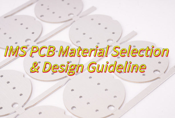
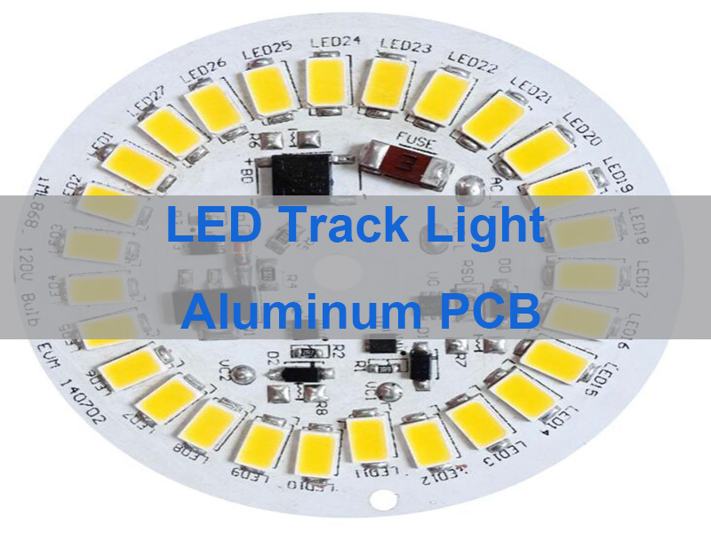
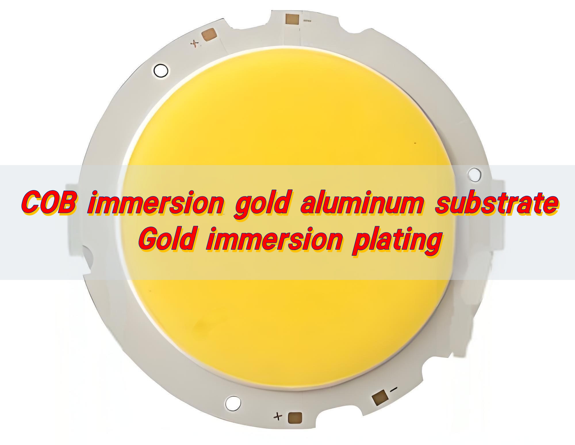
IMS PCB low volume manufacturer services help engineers build and verify thermal boards before committing to higher production quantities. Standard one-layer MCPCB prototypes can be completed in four days under normal service, with 24-hour service available for urgent orders. Copper-base boards, direct thermal path structures, and other custom requirements need an individual schedule.
EBest Circuit (Best Technology) supports IMS PCB prototypes and small batches through PCB fabrication, component sourcing, PCBA, and testing. For an accurate quote, identify the quantity, material, critical dimensions, and expected repeat demand.
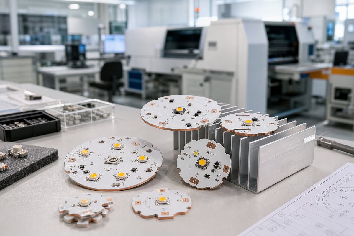
What Should You Confirm With an IMS PCB Low Volume Manufacturer?
Ask the manufacturer to answer five questions in writing:
- Can you build this exact IMS structure?
- Which requirements are standard, and which need material or process confirmation?
- When does the quoted lead time start?
- Will production files be sent back for approval before fabrication?
- Which reports will ship with the boards?
The following lead times apply to standard MCPCB prototypes under 1 m² using standard aluminum, 0.8–2.0 mm board thickness, H/H or 2 oz copper, lead-free HASL, white solder mask, black silkscreen, and 0.8 W/m·K thermal conductivity.
| Standard prototype reference | Standard service | Fastest service |
|---|---|---|
| 1-layer MCPCB | 4 days | 24 hours |
| 2-layer MCPCB | 14 days | 168 hours |
| 4-layer MCPCB | 21 days | Confirm per project |
Custom copper-base or direct thermal path boards require a project-specific schedule. EBest assigns one business contact and three engineering roles covering R&D, PCB process, and PCBA, so commercial and technical questions can be handled together.
Which Insulated Metal Substrate PCB Specs Control Cost and Risk?
The quotation should define the complete thermal stack, not just “aluminum PCB” or “copper IMS.” The metal base spreads heat; the dielectric transfers heat while maintaining electrical insulation.
The most important quotation specifications are:
- metal-base type and thickness;
- dielectric thermal conductivity, thickness, and insulation requirement;
- layer construction and copper weight;
- finished board thickness and critical mechanical tolerances;
- surface finish, solder mask, and silkscreen;
- electrical test and any project-specific report.
Thermal conductivity cannot be compared alone. Dielectric thickness, insulation, operating voltage, heat source, and the heat-sink interface matter together. Copper weight also changes trace geometry and cost: routine inner copper options include 0.5–3 oz, while routine outer copper options include 1–3 oz.
How Does Metal Core PCB Material Choice Affect a Small Batch?
In a low-volume build, material availability and minimum sheet purchases can affect unit cost. Aluminum balances heat spreading, weight, machining, and price. Copper spreads heat more effectively but is heavier and more expensive. Direct thermal path structures are used when the design needs a shorter route from the heat source to the metal base.
Material choice should answer four practical questions:
- Does it move enough heat for the real operating load?
- Does the dielectric meet the electrical insulation requirement?
- Is the selected thickness compatible with the housing and heat sink?
- Can the same material be obtained for the next build?
Provide both the current quantity and expected repeat demand. This helps engineering assess panel use and purchasing check material continuity. If assembly is required, component sourcing and PCBA are scheduled separately; prototype PCBA can typically be delivered in about 1.5 weeks, subject to BOM and test requirements.
What Files Does an IMS PCB Manufacturer Need for Quotation?
Gerber data defines the circuit pattern, but not always the complete material, mechanical, and inspection requirements. A clear quotation package avoids repeated questions and incorrect assumptions.
A complete bare-board package normally includes:
- Circuit data: Gerber or ODB++ and NC drill files;
- Mechanical data: board outline, holes, slots, dimensions, and tolerances;
- Material data: metal base, dielectric requirement, copper weight, and finished thickness;
- Finish data: surface finish, solder mask, silkscreen, and marking requirements;
- Order data: quantity, delivery format, target date, and required reports.
Use the same project name and revision across all files. Conflicting copper, finish, outline, or thickness information can produce an inaccurate quote.
For PCBA, add:
- BOM with manufacturer part numbers and approved alternatives;
- pick-and-place data and assembly drawing;
- polarity and orientation notes;
- programming and functional-test requirements;
- special inspection requirements for hidden or high-risk joints.
EBest’s DFM pre-review covers manufacturing data, materials, panelization, component spacing, assembly process, and test access. BOM review can also flag long-lead, obsolete, or alternative components before they delay the build.
Which Checks Reduce Risk in Small-Batch IMS Production?
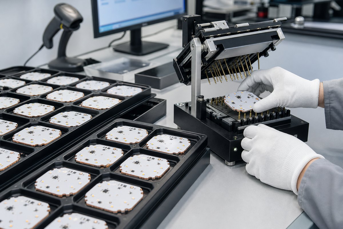
The most useful control is inspection before the remaining value is added.
Before the remaining quantity proceeds, review:
- material and stack-up confirmation;
- critical mounting and outline dimensions;
- electrical-test status;
- surface finish and solder-mask condition;
- fit with the heat sink, enclosure, or assembly fixture.
Electrical testing checks continuity and isolation. Required records—such as an electrical test report, COC, or dimensional report—should be agreed before production.
For PCBA, select inspection according to the design. AOI covers visible defects; X-ray is used when joints are hidden beneath packages such as BGA or CSP.
The inspection method should match the defect:
- SPI: solder-paste volume, area, height, offset, and bridging;
- First-piece verification: component value, polarity, and placement setup;
- AOI: visible component and solder-joint defects;
- X-ray: hidden BGA, CSP, or bottom-terminated joints;
- Functional test: product behavior against customer-defined limits.
The digital workshop can retrieve key material, batch, cycle, and progress records within five seconds, supporting faster quality investigation.
IMS PCB Case Study: From Prototype to Repeat Order
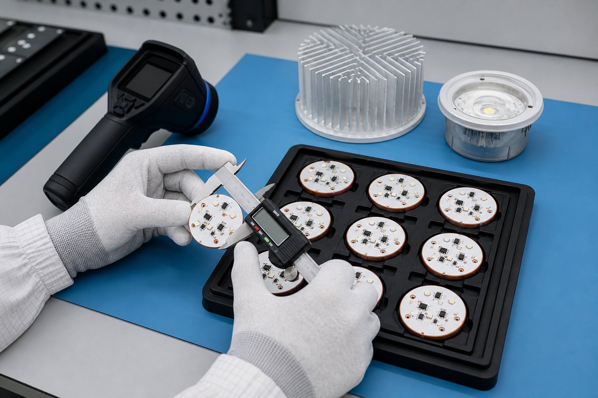
A U.S. engineering team was developing a compact high-power LED lighting module. The LEDs generated concentrated heat, so a conventional aluminum IMS board did not provide the heat path required by the mechanical design. The project therefore used a single-sided thermoelectric-separation copper-base PCB.
Project snapshot
- Application: high-power LED lighting module
- Customer location: United States
- Prototype quantity: 10 pcs
- Repeat order: 500 pcs after prototype validation
- Sample production lead time: 10 working days
- Repeat-order production lead time: 15 working days
- Lead-time basis: production only, counted after material and production-file approval; international shipping excluded
PCB requirements
- 1.5 mm copper base
- 3 W/m·K adhesive film, 100 μm thick
- Pure adhesive lamination not permitted
- 2 oz copper
- White solder mask and black silkscreen
- OSP surface finish
- Individual-board delivery
- Production files submitted for customer approval before fabrication
- COC and electrical test report supplied with shipment
The engineering risk was concentrated in the thermal interface. The 3 W film had to remain 100 μm thick, and pure adhesive could not be substituted because it would create a different thermal and insulation structure. The production data therefore identified the copper-base structure, dielectric film, copper, finish, and delivery format for approval before the first panel was released.
Ten prototype boards were produced in 10 working days. The customer used them to check:
- LED mounting and polarity;
- mechanical fit with the module housing;
- contact between the copper base and heat-spreading surface;
- temperature behavior during the lighting test;
- solderability and electrical performance.
After prototype validation, the customer placed a 500-piece repeat order. The approved production revision and material requirements were retained, avoiding another interpretation cycle. Production was completed in 15 working days, and the boards were delivered individually with the agreed COC and electrical test report.
The value of the prototype was not only proving that the circuit worked. It confirmed the material system, thermal interface, manufacturing files, inspection records, and delivery format before the larger order.
How Do You Compare IMS PCB Low Volume Manufacturers?
Compare the answers to these five questions:
| Buyer question | Strong answer | Weak answer |
|---|---|---|
| Is my construction understood? | The quotation repeats the metal base, dielectric, copper, finish, and delivery format | “Standard IMS PCB” |
| Is the lead time applicable? | It states the starting point, material status, fabrication time, and shipment point | A fastest-day claim with no conditions |
| Will engineering review my files? | Written DFM questions and production files are returned for approval | “Files checked” with no review output |
| What evidence will I receive? | COC, electrical test report, and any project-specific record are named | “Quality guaranteed” |
| Can you support the next stage? | Prototype, repeat PCB, sourcing, PCBA, testing, and change control are separated clearly | A one-time prototype quote with no continuity plan |
EBest operates its own PCB and PCBA factories, works with more than 1,000 supply-chain partners, and holds ISO 9001, ISO 13485, IATF 16949, and AS9100D certifications. Its integrated team supports prototypes, repeat PCB orders, sourcing, assembly, testing, and traceability.
FAQs About IMS PCB Low Volume Manufacturer
Can a standard MCPCB lead time be used for every low-volume IMS board?
No. Published standard lead times apply only under the stated material and process conditions. Copper-base, direct thermal path, special dielectric, unusual finish, tight tolerance, or extra report requirements need project-specific confirmation.
Does EBest Circuit accept prototype and small-batch IMS orders?
Yes. EBest supports prototype and small-batch projects, with the actual quotation based on construction, material availability, quantity, panel use, inspection, and delivery requirements.
What should a manufacturer confirm about an IMS dielectric?
Confirm the material or approved equivalent, thermal conductivity, dielectric thickness, insulation requirement, lamination system, availability, and whether substitution requires written approval.
Why approve production files before fabrication?
Production-file approval lets the customer check how the factory interpreted the stack-up, material, copper, finish, mechanical details, delivery format, and documentation before irreversible work begins.
Should COC and an electrical test report be requested in the RFQ?
Yes, when they are required. Naming them in the RFQ and purchase order makes them controlled shipment deliverables instead of assumptions.
Ready to work with an IMS PCB low volume manufacturer? Send your Gerber files, quantity, metal-base and dielectric requirements, copper weight, finish, critical dimensions, and required reports to sales@bestpcbs.com. EBest’s engineering team will review the project and provide a practical quotation and production plan.