





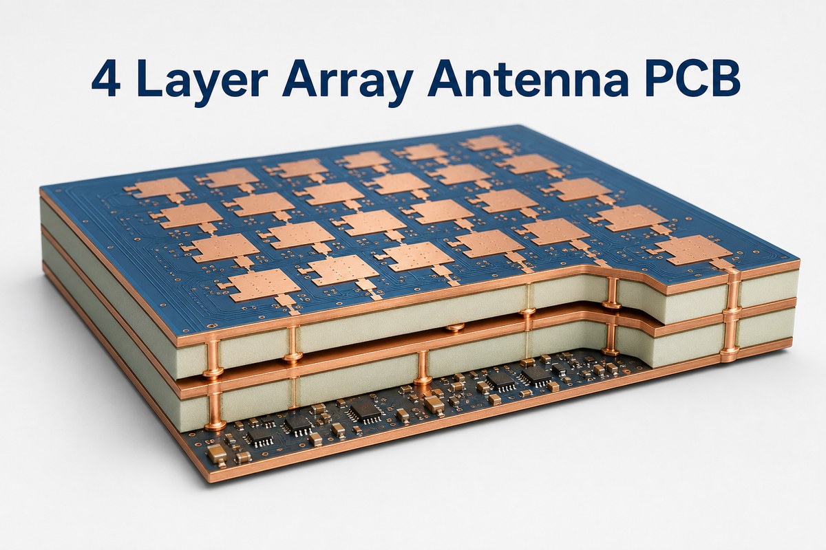
A 4 layer array antenna PCB combines antenna elements, controlled RF paths, reference planes and support circuitry in one board. Its measured performance depends on the manufactured stackup as much as the simulated antenna geometry.
Here, “4 layer” means four copper layers. It does not describe a four-element or 4 × 4 array. The final construction must match the operating frequency, antenna architecture and validation plan.
EBest Circuit provides multilayer RF and high-frequency PCB fabrication, impedance-control support, prototypes, small-volume production and PCB assembly. Send us your stackup, material requirements, impedance table, quantity and production data for review and quotation.
What Is a 4 Layer Array Antenna PCB?
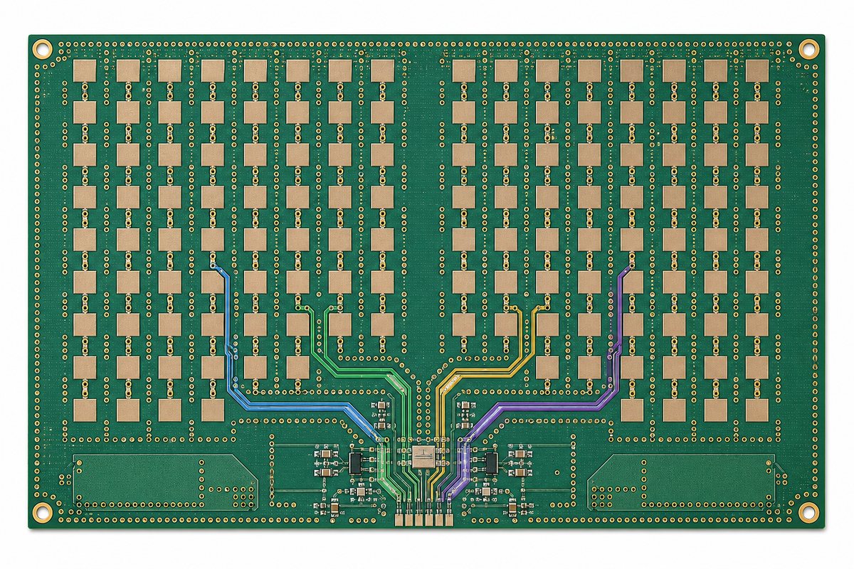
A four-layer array antenna PCB is an RF board with several coordinated radiating elements and a shared feed or beamforming network. The copper layers divide antenna, reference, power, control and component-routing functions.
A passive array may use a fixed feed network. A phased array antenna PCB also controls channel phase and often amplitude. PCB layer count and antenna element count are separate design decisions.
| Term | Meaning |
| 4 layer PCB | Four copper layers separated by dielectric materials |
| Array antenna PCB | Multiple elements operating as one coordinated aperture |
| Phased array antenna PCB | An array with controlled channel phase and usually amplitude |
What Is a Phased Array Antenna, and How Does It Work?
A phased array antenna forms and steers a beam by controlling the relative phase of its elements. Constructive interference strengthens radiation in the target direction, while cancellation shapes sidelobes and nulls.
How does a phased array antenna work on a PCB? Each RF channel adds delay and loss through its trace, dielectric, vias, components and connector launch. Small physical differences therefore become channel errors.
Calibration can correct limited residual error, but it cannot replace repeatable PCB construction. Large mismatches reduce calibration margin and increase sensitivity to temperature and production variation.
What Does Each Copper Layer Do?
Each copper layer needs one clear primary role before routing starts. The arrangement below is a practical baseline, not a universal antenna stackup.
| Layer | Typical Role | Main Check |
| L1 | Patch elements, microstrip feeds or RF components | Element geometry and spacing to reference |
| L2 | Continuous RF ground or reference | Return-path continuity |
| L3 | Power, bias and low-speed control | Isolation from sensitive RF regions |
| L4 | RF components, exits and control routing | Component density and transition geometry |
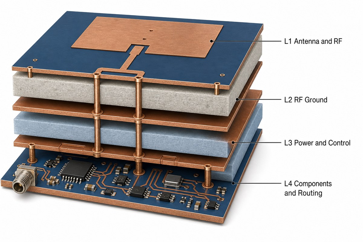
Aperture-coupled and proximity-coupled antennas may assign the layers differently. Confirm finished dielectric thickness, processed copper and coupling geometry in the electromagnetic model before freezing the layout.
Which Materials and Copper Profiles Suit the Operating Frequency?
The laminate must keep dielectric behavior and conductor loss predictable across the operating band. Frequency matters, but bandwidth, efficiency, phase consistency, availability and fabrication process also affect the choice.
FR-4 may suit lower-frequency or narrowband designs when its measured variation and loss are acceptable. Microwave and millimeter-wave arrays often need controlled design Dk, low Df, stable thickness and suitable copper roughness.
- Use supplier-supported design Dk at the relevant frequency.
- Specify finished dielectric thickness.
- Include copper roughness in loss modeling.
- Confirm laminate, bondply, foil and finish compatibility.
- Keep one approved construction from prototype through production.
How Should Feed Lines, Reference Planes and Vias Be Designed?
RF feeds need field-solved geometry and an uninterrupted reference path. A nominal 50 Ω target does not define one trace width because impedance changes with Dk, dielectric thickness, copper and local geometry.
Keep bends, tapers, pads and layer transitions consistent across matched channels. Avoid plane splits beneath critical paths, and place return vias close to signal transitions without disturbing the antenna field.
Via fencing can reduce coupling, but arbitrary dense stitching can detune the antenna. Treat via stitching as part of the RF model rather than a final layout cleanup step.
How Should Element Spacing and Channel Symmetry Be Controlled?
Array pitch must follow wavelength, scan range and element pattern. It is not a generic PCB spacing value. Edge elements also need separate review because they see a different electromagnetic environment.
Matched channels need the same reference plane, transition count, bend geometry and connector launch. Equal trace length alone cannot compensate for different vias, clearances or nearby copper.
- Verify one unit cell before replication.
- Lock antenna, feed and ground geometry together.
- Keep solder mask conditions consistent around each element.
- Model packages and connectors that add phase or loss.
Which Fabrication Tolerances Need Explicit Control?
Control dimensions that change impedance, resonance, coupling or channel balance. General PCB tolerances may be too broad for RF-critical geometry, so the fabrication drawing must identify those features.
| Feature | RF Effect | Required Record |
| Finished dielectric thickness | Impedance, coupling and resonance | Approved finished stackup |
| RF trace and gap geometry | Impedance and phase delay | Impedance table and coupon plan |
| Patch size and registration | Resonance and element consistency | Critical-dimension notes |
| Copper thickness and profile | Loss and impedance | Approved foil and finished copper |
| Via geometry | Transition inductance and return path | Hole, pad and antipad requirements |
Use the impedance control PCB documentation as a starting point, then add antenna-specific dimensions. Confirm the producible stackup before final RF tuning.
When Is a Four-Layer Stackup Not Enough?
Four layers are insufficient when routing, isolation, power distribution or thermal paths disturb the antenna aperture and its references. Adding layers can reduce compromise, but it changes transitions, thickness and cost.
Consider more layers for dense beamformer fanout, several isolated RF paths, multiple power rails, high-speed control, buried aperture routing or separate shielding cavities. Hybrid construction may help when RF and control regions need different materials.
The choice must follow the complete layout and EM model. Moving a path into stripline may improve isolation but add via loss, so evaluate the stripline versus microstrip trade-off at the project frequency.
How Should Assembly and Thermal Design Protect RF Performance?
Assembly must preserve the grounding, geometry and channel balance established by the bare PCB. Use package-specific land patterns and stencil design, especially under exposed pads and dense RF components.
Control solder volume and voiding where the package requires it. Ground and thermal vias must support the component without creating an unmodeled coupling path near the antenna.
Plan heat removal before final RF routing. Uneven temperature can shift gain and phase, while heat spreaders and mechanical supports can disturb the aperture if they enter an RF keepout region.
How Should the Board Be Tested Before OTA Validation?
Verify construction and RF paths before over-the-air testing. OTA measurements evaluate the radiated system, but they are inefficient for finding an open via, incorrect stackup or poor connector launch.
- Review material records and the finished stackup.
- Complete continuity and isolation testing.
- Inspect registration, RF features, mask and vias.
- Measure representative impedance coupons.
- Use a VNA for return loss and channel comparison.
- Run planned OTA pattern and scan validation.
- Compare several boards from the same revision.

Coupons cannot prove patch resonance, coupling or beam shape. Keep coupon, VNA and OTA results linked to the same board revision and production lot.
FAQ About 4 Layer Array Antenna PCB Projects
Can FR-4 be used for an array antenna PCB?
Yes, when measured dielectric variation and loss meet the operating-band requirement. Do not assume that every FR-4 grade behaves the same.
Should solder mask cover the patch elements?
Only when the model includes its dielectric effect. An unplanned coating change can shift resonance.
Which surface finish is best?
No finish is universal. Compare RF loss, thickness, planarity, solderability and assembly needs before approval.
Can impedance coupons verify the antenna?
No. Coupons verify representative transmission lines, while the complete antenna still needs VNA and OTA validation.
Does the PCB manufacturer need OTA equipment?
Not necessarily. The manufacturer controls construction and electrical integrity; the antenna team can own final calibration and OTA acceptance.
How Can EBest Circuit Support Your Array Antenna PCB?
At EBest Circuit, we support multilayer RF and high-frequency PCB fabrication, controlled impedance, prototypes, small-volume production and PCB assembly. Our PCB checks can include electrical testing, impedance testing and micro-section inspection.
Send your Gerber or ODB++ data, drill files, stackup, target frequency, materials, impedance requirements, quantity and assembly package to sales@bestpcbs.com. We will review the manufacturing data and prepare a quotation.
You may also like






Tags: 4 layer array antenna PCB, array antenna pcb, how does a phased array antenna work, phased array antenna pcb, what is a phased array antenna