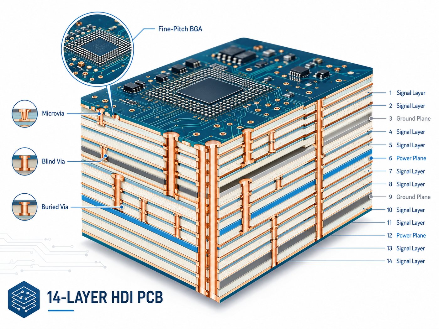
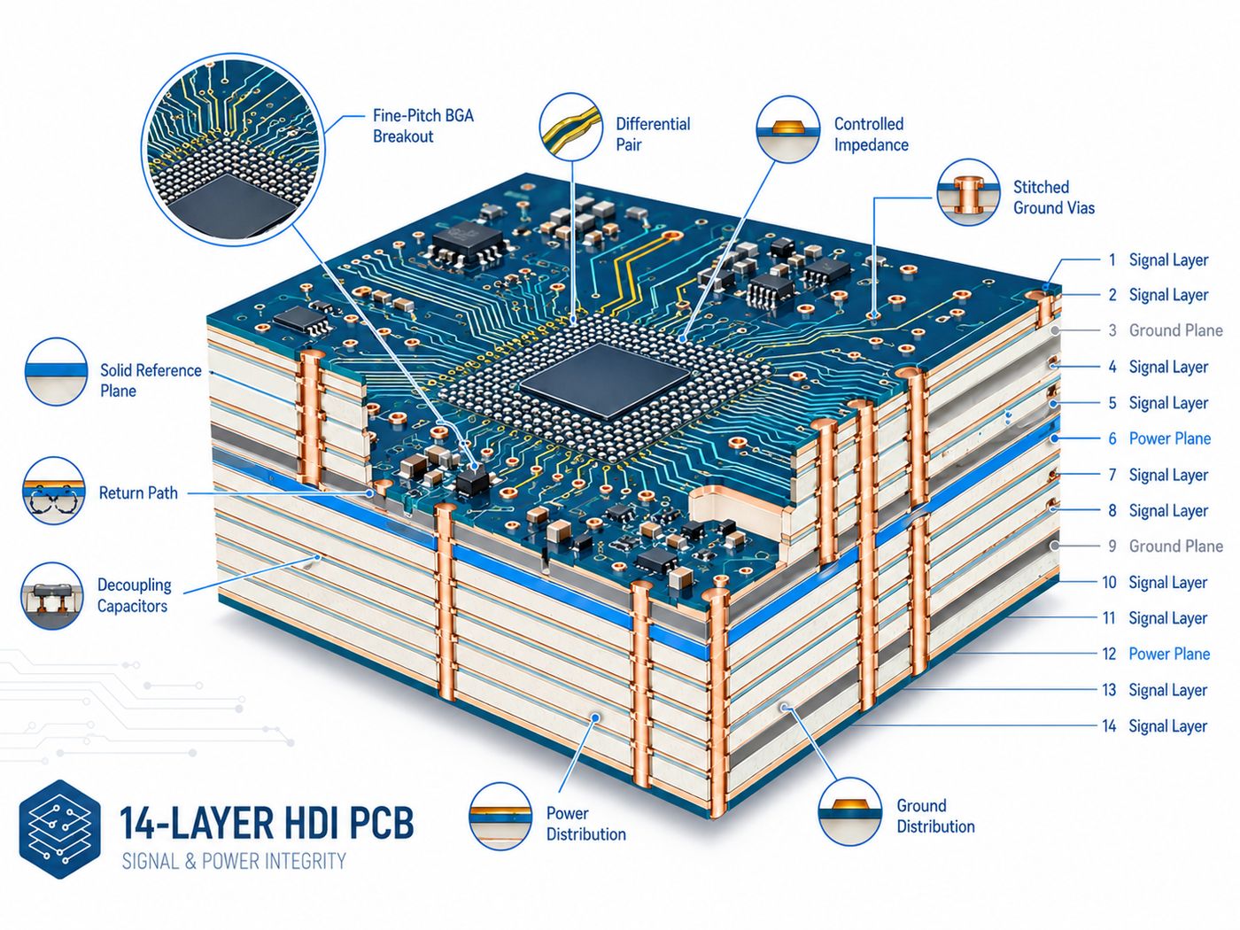
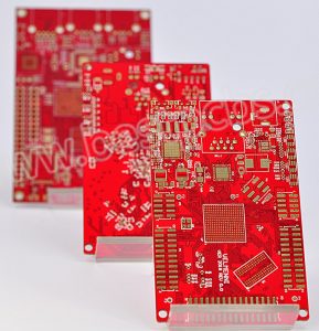
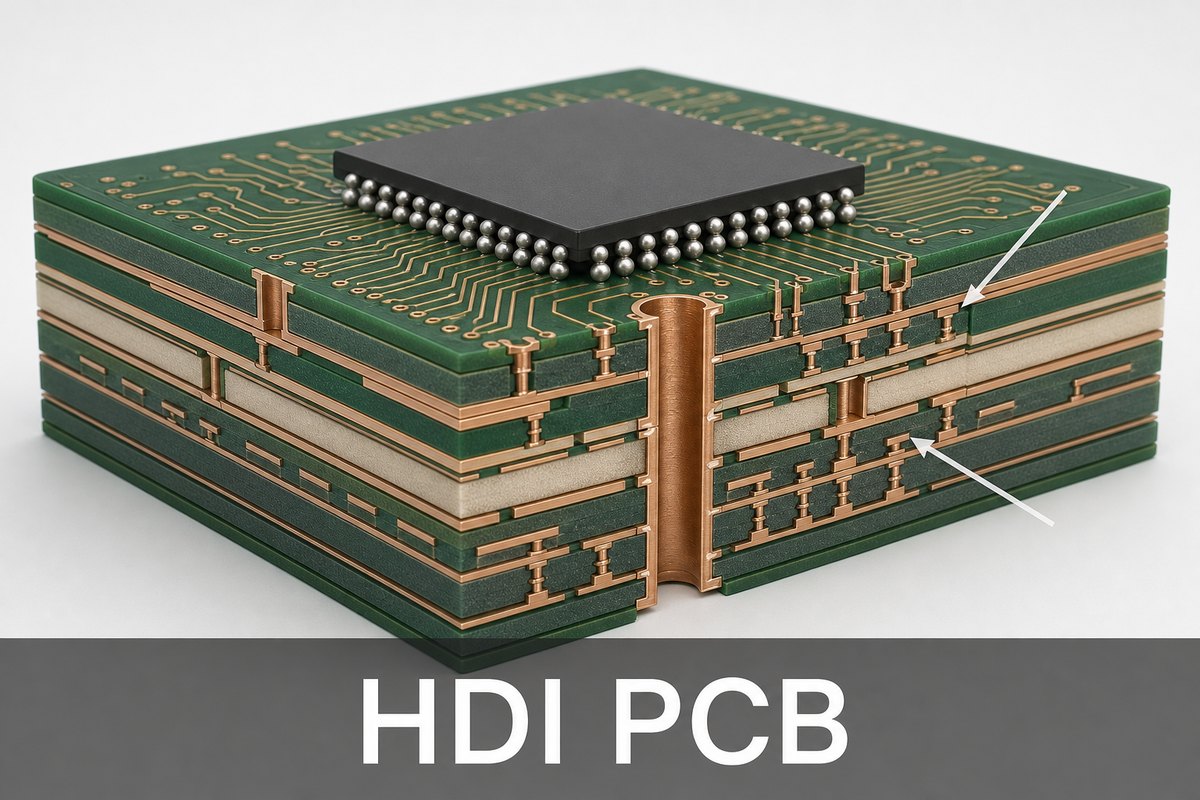
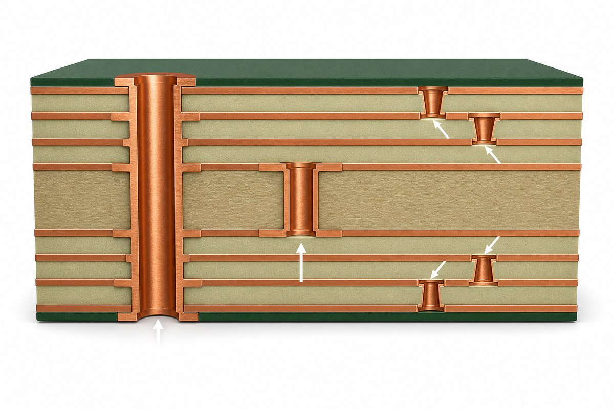
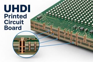
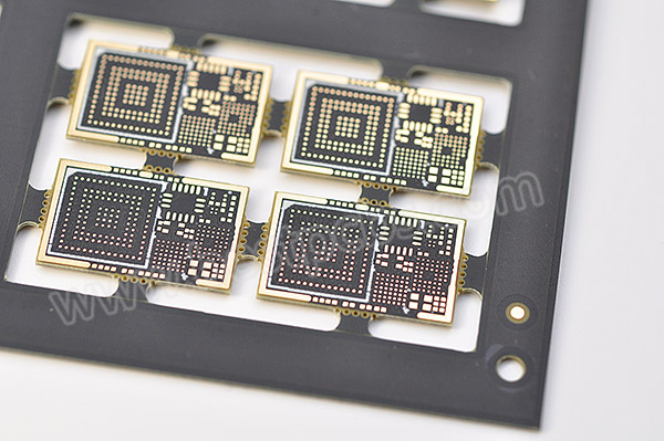
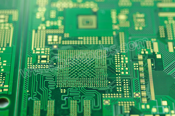
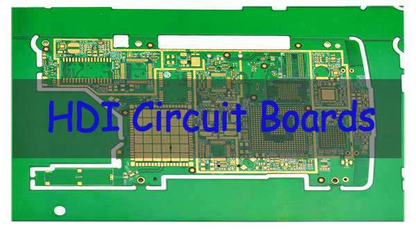
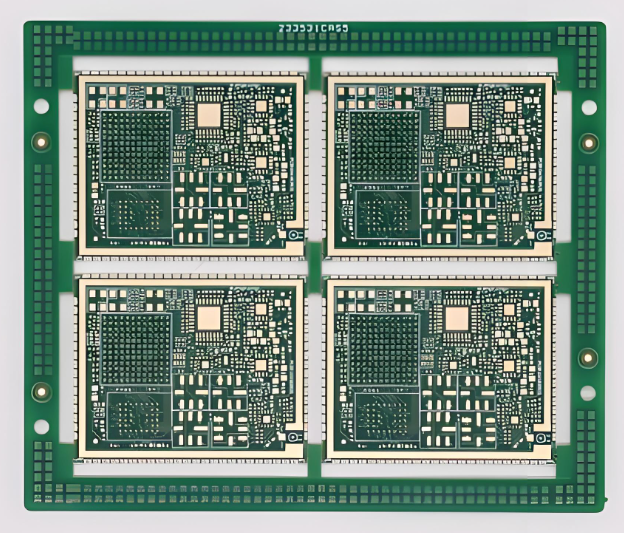
A 14 layer HDI PCB combines 14 copper layers with high-density interconnect features such as microvias, blind and buried vias, sequential lamination, and via-in-pad.
The extra layers provide room for signals, ground planes, and power distribution. HDI technology solves the routing problem around fine-pitch components, where conventional through vias consume too much board space.
Before selecting this structure, engineers usually need to determine:
How many HDI buildup layers are necessary?
Can the BGA be routed without stacked microvias?
Which stackup supports the required impedance?
Can the laminate tolerate repeated lamination?
Which fabrication limits should be confirmed before layout is frozen?
These choices have a larger impact on cost and manufacturability than the layer count alone.
What Is a 14-Layer HDI PCB?
A 14-layer HDI PCB has 14 conductive copper layers and uses high-density vias to connect selected layers.
Common HDI features include:
Laser-drilled microvias
Blind and buried vias
Via-in-pad
Stacked or staggered microvias
Sequential buildup layers
A conventional 14 layer PCB can also have 14 copper layers but rely mainly on through vias.
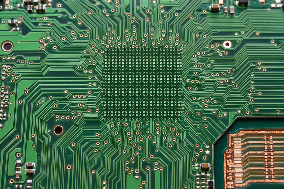
HDI becomes useful when a design needs more routing channels around fine-pitch BGAs, processors, FPGAs, or other dense packages. If component pitch is generous and board area is not constrained, a conventional multilayer board may be the more economical choice.
When Do You Need a 14-Layer HDI PCB?
A 14-layer HDI construction makes sense when routing density, board size, and electrical requirements begin competing for the same space.
Typical cases include:
Fine-pitch BGA breakout
High-I/O processors or FPGAs
Compact communication or computing boards
Multiple high-speed interfaces
Designs requiring several continuous reference planes
Dense layouts where through vias block inner-layer routing
HDI should solve a specific layout problem. If a standard 14-layer board can meet routing and electrical requirements without microvias or sequential buildup, adding HDI only increases fabrication complexity.
How Is a 14-Layer HDI PCB Stackup Designed?
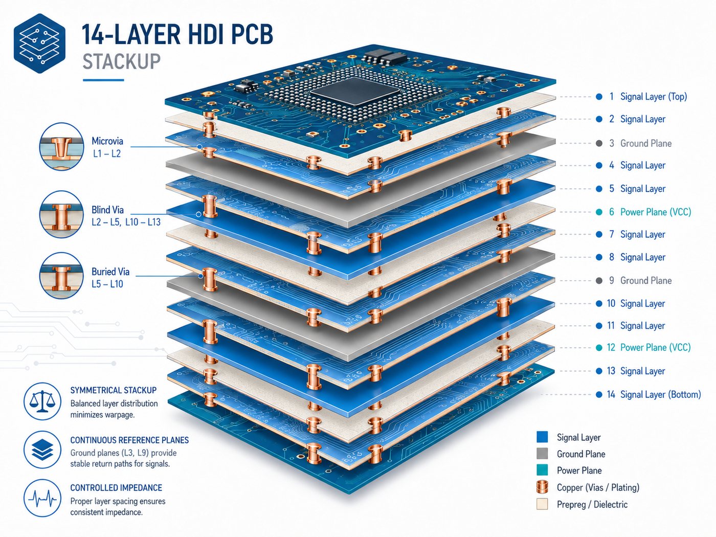
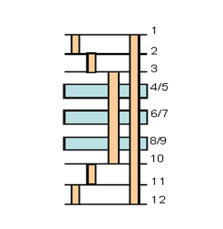
A 14 layer PCB stackup should be built around routing, impedance, power distribution, board thickness, and via structure.
The HDI PCB stackup must be reviewed with the approved laminate system, finished thickness, copper distribution, and impedance targets before routing is released.
This is an example, not a universal stackup. Actual dielectric thickness, copper weight, and layer assignment depend on the design.
Three practical rules are useful:
Keep high-speed signal layers next to continuous reference planes.
Maintain a reasonably symmetrical construction to reduce warpage risk.
Define the HDI layer stackup together with the microvia structure.
For example, if microvias connect L1-L2 and L2-L3, the dielectric thickness between those layers must suit the selected laser-via geometry. Stackup review should therefore happen before final routing.
Which HDI Buildup Structure Should a 14-Layer PCB Use?
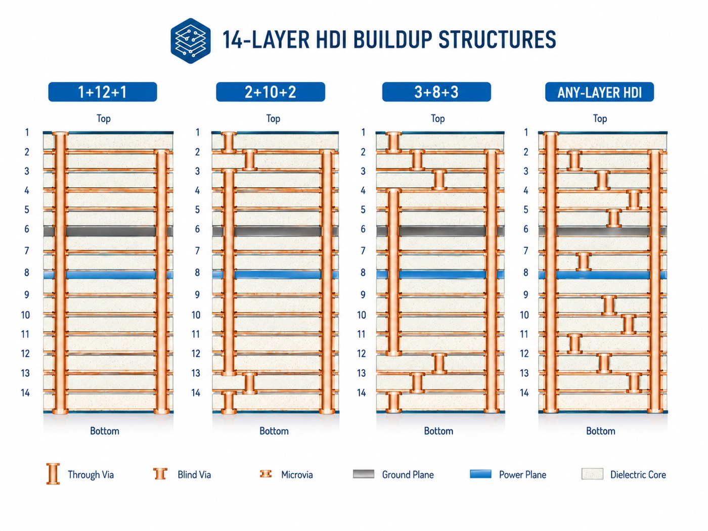
The buildup defines how many HDI layers are added around the central multilayer structure.
Structure
Typical Use
1+12+1
Moderate-density outer-layer breakout
2+10+2
Higher-density BGA routing
3+8+3
Very dense component areas
Any-layer HDI
Designs requiring maximum interconnection flexibility
A 1+12+1 structure is suitable when signals mainly need to move from the outer layer into the first internal routing layer.
A 2+10+2 structure provides more routing freedom around dense BGAs or processors.
Moving to 3-step or any-layer HDI should have a clear routing benefit. More buildup stages mean additional lamination, laser drilling, plating, filling, and registration control. The best structure is usually the simplest one that completes the routing without compromising electrical requirements.
How Should Microvias, Blind Vias, and Buried Vias Be Used?
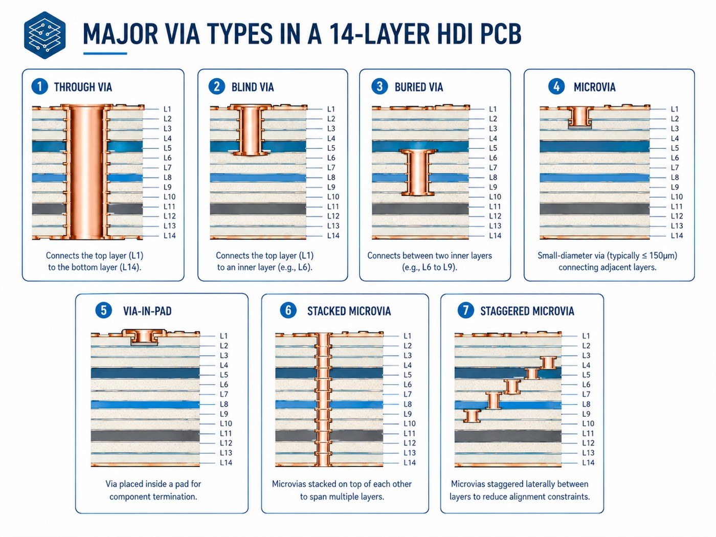
Each via type has a different job.
Via Type
Best Use
Through via
General connections in lower-density areas
Blind via
Outer-to-inner layer connections
Buried via
Internal layer-to-layer routing
Microvia
Fine-pitch routing between nearby layers
Via-in-pad
BGA and small-package breakout
Stacked microvia
Maximum routing density
Staggered microvia
Multi-level routing where offset space is available
Stacked microvias save space but require tighter control of:
Copper filling
Layer registration
Plating quality
Thermal reliability
Staggered microvias are often easier to manufacture when the layout has enough space for an offset transition.
Via-in-pad is useful under fine-pitch BGAs. These vias normally need to be filled and planarized so the component pad remains flat and solderable.
What Are the Key 14-Layer HDI PCB Design Rules?
These HDI PCB design guidelines should match the manufacturer’s actual production capability rather than a generic CAD rule set.
Confirm these items before layout is finalized:
Microvia diameter and depth
Capture-pad size
Annular ring
Minimum trace and space
Via-to-pad clearance
Via filling requirements
Stacked microvia capability
Layer registration tolerance
Controlled impedance
Avoid using the factory’s absolute minimum geometry across the entire board. A feature that can be produced in a small isolated area may not be the best choice for stable volume production.
Copper balance should also be considered across the stack. Large differences in copper distribution between corresponding layers can increase warpage risk.
For controlled impedance, provide the target values and net types. Trace dimensions can then be adjusted against the actual laminate and finished dielectric thickness.
How Do You Control Signal and Power Integrity in a 14-Layer HDI PCB?
Fourteen layers provide useful flexibility for signal and power planning, but only if the reference structure is well organized.
For signal integrity:
Route high-speed traces next to solid reference planes.
Avoid routing across plane splits.
Keep differential-pair geometry consistent.
Add nearby ground vias when signals change reference layers.
Use short microvia transitions where appropriate.
Avoid unnecessary through-via stubs.
For power integrity:
Provide low-inductance paths between power and ground.
Keep critical power planes close to their return planes where practical.
Place decoupling close to high-current and fast-switching devices.
Avoid fragmented return paths around plane cutouts.
The benefit of a 14-layer structure is not simply “more layers.” It is the ability to separate routing, reference, and power functions without forcing too many compromises.
Which Materials Are Suitable for a 14-Layer HDI PCB?
Material choice depends on electrical loss, thermal stress, and repeated-lamination requirements.
Material Type
Typical Fit
High-Tg FR-4
General industrial HDI
Low-loss FR-4
Higher-speed digital designs
High-performance laminate
Demanding thermal or reliability requirements
Hybrid stackup
Designs where only selected layers need special properties
Important parameters include:
Tg
Z-axis CTE
Dk
Df
Resin system
Moisture behavior
Repeated-lamination performance
For high-speed designs, Dk and Df affect impedance and transmission loss. For multilayer HDI, Z-axis expansion and laminate stability also matter because vias experience repeated thermal stress during fabrication and assembly.
Material availability should be checked before quotation. An uncommon laminate can add unnecessary sourcing time even when the PCB design itself is straightforward.
How Is a 14-Layer HDI PCB Manufactured?
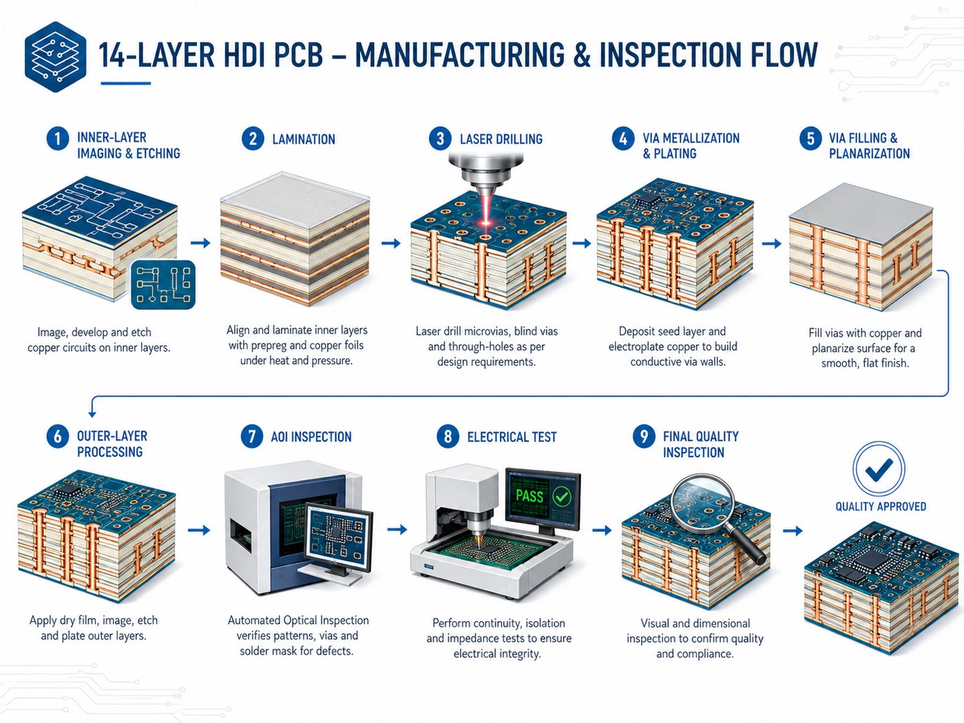
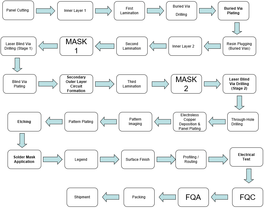
The HDI PCB manufacturing process for a 14-layer board adds sequential buildup steps to conventional multilayer fabrication.
A simplified flow is:
Inner-layer imaging and etching
AOI inspection
Core lamination
Buried-via processing if required
Buildup dielectric lamination
Laser drilling
Via metallization and plating
Via filling and planarization where required
Additional buildup cycles
Outer-layer processing
Solder mask and surface finish
Electrical and final inspection
A 2+N+2 structure repeats the buildup and laser-drilling sequence for the second HDI level.
The main manufacturing challenge is maintaining alignment and via quality through repeated processing. A factory capable of standard 14-layer PCBs is therefore not automatically qualified for complex HDI builds.
How Is 14-Layer HDI PCB Reliability Verified?
Electrical testing confirms continuity, but HDI also requires inspection of internal interconnects.
Our broader PCB testing guide explains how electrical and inspection methods complement one another.
Method
Main Purpose
AOI
Conductor and pattern inspection
Electrical test
Open and short detection
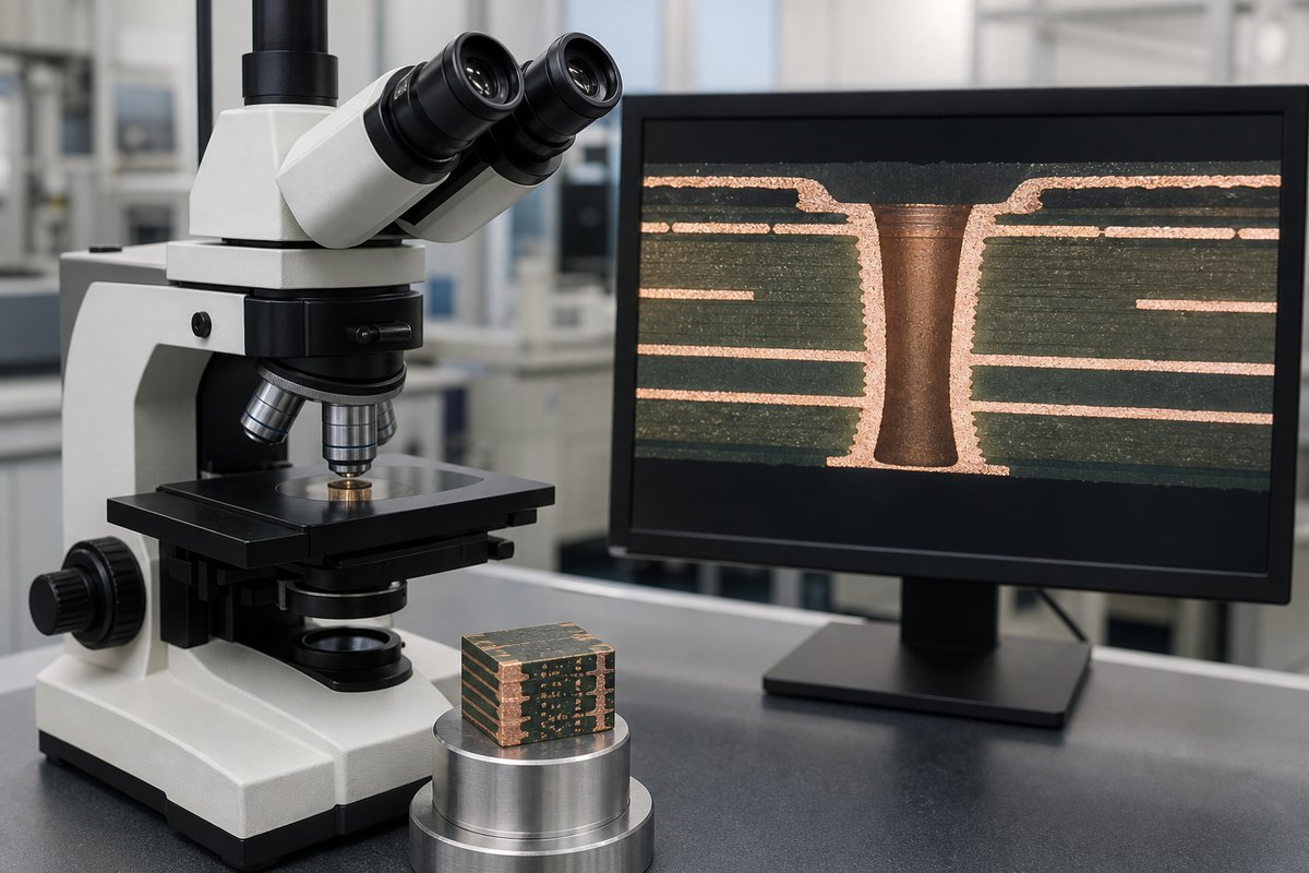
Microsection
Via plating, fill, and registration
Impedance coupon
Controlled impedance verification
X-ray
Selected internal structure inspection
Thermal testing
Interconnect behavior under temperature stress
Dimensional inspection
Alignment and finished geometry
Microsection inspection is particularly useful for stacked or filled microvias because the critical structure is hidden inside the PCB.
For high-reliability projects, define acceptance class, coupon requirements, thermal testing, and reporting requirements at RFQ stage. These items can affect both panel design and quotation.
What Affects 14-Layer HDI PCB Cost and Lead Time?
HDI architecture often affects price more than the difference between conventional multilayer counts.
Cost Driver
Why It Matters
Sequential lamination
Adds fabrication cycles
Stacked microvias
Requires tighter registration and filling control
Fine line/space
Reduces process margin
Via-in-pad filling
Adds filling and planarization
Specialty laminate
Raises material or sourcing cost
Tight impedance
Requires engineering and verification
Additional reliability tests
Adds inspection and qualification
Small prototype quantity
Setup cost is spread over fewer boards
One effective way to control cost is to simplify the via structure.
If a 2+10+2 construction completes the routing, moving to 3+8+3 simply for extra flexibility is usually difficult to justify.
When comparing quotes, make sure each supplier is pricing the same material, stackup, microvia structure, surface finish, and testing requirements.
How Do You Choose a 14-Layer HDI PCB Manufacturer?
Do not qualify a supplier only by checking whether its capability table says “14 layers” or “HDI.”
Confirm the processes that your design actually requires:
Sequential lamination
Laser-drilled microvias
Copper-filled via-in-pad
Stacked or staggered microvias
Fine line and space
Controlled impedance
Layer registration
Microsection inspection
Electrical testing
The manufacturer’s DFM feedback should also be specific. If an engineer suggests changing a stacked microvia to a staggered one, the reason should be clear—whether it is reliability, process margin, cost, or production capability.
For quotation, provide:
Gerber or ODB++ data
Drill files
Preferred stackup, if available
Material requirement
Finished board thickness
Copper weight
Impedance requirements
Microvia and via-in-pad details
Surface finish
Test requirements
Prototype and production quantities
If the stackup is still open, provide the electrical and mechanical requirements instead.
At EBest Circuit, reviewing the stackup and via structure before layout is locked gives engineers more room to resolve manufacturing issues without forcing major redesign later.
Frequently Asked Questions About 14-Layer HDI PCBs
Is every 14-layer PCB an HDI PCB?
No. Fourteen layers describe the copper-layer count. HDI describes the interconnection technology. A 14-layer board can still be a conventional multilayer PCB.
What is a typical 14-layer HDI PCB stackup?
There is no universal stackup. Structures such as 1+12+1 and 2+10+2 are possible, but the final choice depends on BGA routing, impedance, board thickness, and required HDI layers.
What is the difference between a 14-layer HDI PCB and a standard 14-layer PCB?
A 14-layer HDI PCB uses localized high-density connections such as microvias and blind vias. A standard 14-layer PCB may rely mainly on through vias.
Should stacked or staggered microvias be used in a 14-layer HDI PCB?
Use stacked microvias when routing density requires vertical alignment. Use staggered microvias when enough offset space is available and the design does not require the more compact structure.
What files are required to manufacture a 14-layer HDI PCB?
Provide fabrication and drill data plus the stackup or electrical requirements, material, copper thickness, impedance targets, microvia details, via-fill requirements, surface finish, test requirements, and quantity.
How Can EBest Circuit Support Your 14-Layer HDI PCB Project?
At EBest Circuit, we support HDI PCB stackup review, DFM feedback, controlled impedance, laser-drilled microvias, and multilayer PCB fabrication. Send us your Gerber or ODB++ files, stackup, material, finished thickness, impedance targets, via structure, surface finish, test requirements, and quantities for an engineering review and quotation.
An HDI PCB is ready for fabrication only when its package escape, stackup, microvia structure, materials and release data describe one manufacturable system. The most useful design review does not ask whether each feature works in isolation. It checks whether all of those features can be built, inspected and repeated together.
This guide gives hardware designers, PCB layout engineers, quality teams and buyers a practical release sequence. It starts with the reason for using HDI, follows the design through stackup and microvia decisions, and ends with the evidence and files a fabricator needs before production.
What Is an HDI PCB, and When Does a Design Need It?
An HDI PCB is a high-density interconnect board that uses fine conductors and compact interconnect structures to route more connections within limited space. Laser-drilled microvias, blind or buried vias, via-in-pad and sequential build-up layers are common, but the presence of one feature does not automatically make HDI the right choice.
Use HDI when a measurable constraint cannot be solved cleanly with a conventional multilayer construction. Typical triggers include:
A fine-pitch BGA whose inner rows cannot escape through practical mechanically drilled vias.
A fixed board outline that leaves too few routing channels for the required nets.
A thickness limit that makes a larger conventional layer count unsuitable.
Critical connections that benefit from shorter stubs or more controlled layer transitions.
If standard through vias, sensible trace rules and an ordinary multilayer stackup can complete the design, HDI may add lamination cycles and process risk without adding product value.
Design condition
Likely direction
Question to close
Fine-pitch BGA blocks escape channels
Evaluate HDI
Which pin rows require microvia transitions?
Moderate density and enough board area
Keep a conventional multilayer option open
Can through vias finish the routing with margin?
Strict thickness or form-factor limit
Compare build-up alternatives
Can the dielectric and copper system meet the envelope?
HDI has no defined routing benefit
Stop and simplify
What specific constraint does HDI solve?
What Should Be Defined Before HDI PCB Design Begins?
The component field and electrical constraints should be defined before the stackup is frozen. Starting with a familiar build-up recipe can force the design into unnecessary microvia levels or leave critical BGA rows without a valid escape path.
Prepare a short constraint map that records:
BGA pitch, pad size, pin-row count and permitted fan-out direction.
Signal groups, differential pairs, clocks and sensitive analog nodes.
Power and ground pin distribution, current demand and thermal paths.
Board outline, connector positions, keepouts and mechanical height limits.
Target finished thickness, copper needs and controlled-impedance nets.
Whether via-in-pad is necessary or dog-bone fan-out remains practical.
Route a representative dense area before committing the complete board. This early escape study shows how many build-up layers are genuinely needed and whether placement changes could remove an entire lamination cycle.
How Should an HDI PCB Stackup Be Reviewed?
An HDI PCB stackup should be reviewed as a layer-by-layer connection map, not as shorthand alone. Labels such as 1+N+1 or 2+N+2 describe the number of outer build-up layers, but they do not define dielectric materials, copper thickness, via spans or finished-board tolerances.
Read the proposed construction from the outside inward and confirm every copper layer, dielectric, core, microvia span, buried structure and lamination stage.
Review item
What should be confirmed
Why it matters
Build-up layers
Each added layer solves a documented routing or connection need
Unnecessary cycles add cost and registration interfaces
Dielectrics
Material family, thickness and resin behavior are agreed
They influence laser drilling, lamination and impedance
Copper
Base and finished copper are identified by layer
Trace geometry and plating allowances depend on copper condition
Reference planes
Critical signals keep a continuous return path
Plane changes can create return discontinuities
Via spans
Every laser, buried and through-hole span matches the construction
Ambiguous spans cause CAM questions or invalid connections
Finished thickness
Nominal thickness and tolerance include the complete build
Core values alone do not define the finished board
Ask the fabricator to return a proposed production stackup before final impedance routing. A late dielectric substitution can change the required trace width, spacing and coupling geometry.
Which Microvia Structure Should an HDI PCB Use?
An HDI PCB should use the simplest microvia structure that completes the required layer transitions. A single adjacent-layer microvia usually introduces fewer process interfaces than a multi-level stacked structure, while staggered microvias avoid placing several plated interfaces directly above one another.
Stacked microvias can be necessary when escape space is extremely limited, but they require explicit agreement on via filling, target-pad geometry, plating and reliability validation. IPC has warned the electronics industry about latent failures in some complex microvia structures, so a room-temperature continuity test should not be treated as universal proof of long-term reliability.
Identify every laser-drilled, mechanically drilled, blind, buried and through-hole feature.
State which microvias require filling and capping for via-in-pad assembly.
Avoid stacked levels unless the package escape or connection path requires them.
Match microvia depth to the selected dielectric and the fabricator’s qualified process.
Define coupon and thermal-stress expectations for reliability-sensitive products.
The PCB via types guide provides a broader comparison of through, blind, buried and microvia structures.
What HDI PCB Design Guidelines Should Be Confirmed with the Fabricator?
HDI PCB design guidelines should be confirmed for the actual material, copper condition, layer role and via process. A generic minimum-rule table cannot show how several difficult features interact in one design.
Close these items before final routing:
Trace width and spacing by layer and copper thickness.
Laser via diameter, target pad, capture pad and permitted depth.
Via-to-copper, via-to-via and via-to-edge clearances.
Annular-ring and registration allowances for mechanically drilled holes.
Via-in-pad filling, planarization and surface-finish requirements.
Solder-mask definition around fine-pitch component pads.
Copper-density and balancing expectations in dense areas.
Do not combine every published minimum in the same location. A layout that simultaneously uses the smallest trace, spacing, pad and most complex via structure can be substantially harder to manufacture than one with a single controlled challenge.
How Should BGA Escape and Layer Transitions Be Planned?
BGA escape should be planned by pin function, routing layer and return-current path. The shortest geometric route is not necessarily the best electrical route if a layer transition leaves the signal without a nearby reference connection.
Assign outer rows, inner rows, power pins and ground pins before detailed fan-out.
Keep critical nets referenced to continuous planes where practical.
Place an intentional return path near signals that change reference planes.
Maintain differential-pair symmetry through the pad and via field.
Review antipad patterns for power-plane neck-down and current crowding.
Use the proposed production stackup for impedance calculations.
Large processors and FPGAs require a combined signal- and power-integrity review. Dense escape routing may create enough voiding to fragment a plane even when every individual clearance passes the design rules.
How Do Materials, Copper and Thermal Requirements Affect an HDI PCB?
Materials, copper and thermal requirements affect whether the selected build-up can survive fabrication and assembly while meeting electrical performance. Review dielectric thickness, reinforcement, resin behavior, copper profile and finished copper as a coordinated material set.
A lower-loss laminate is not automatically the best option for every HDI layer. The material must also support laser drilling, resin removal, copper adhesion and the planned lamination sequence. Hybrid constructions need additional attention because different material families may move differently during processing.
Thermal analysis should distinguish signal microvias from deliberate heat-transfer structures. Check how heat moves from component pads into planes, filled thermal vias, copper areas, heat spreaders and the enclosure. Do not assume that a dense field of small electrical microvias replaces a designed thermal path.
How Does the HDI PCB Manufacturing Process Affect Design Decisions?
The HDI PCB manufacturing process affects design because each build-up level adds drilling, metallization, imaging, lamination and registration work. The exact route depends on the via map and layer sequence, so the drawing must describe the construction rather than simply state “HDI.”
Fabricate and inspect the inner core or sub-composite.
Create buried interconnects that must be completed before the next lamination.
Laminate the next dielectric and copper layer.
Laser-drill the specified microvias and prepare the hole surfaces.
Metallize, plate and fill the vias required by the design.
Image and etch the added circuit layer.
Repeat the build-up sequence when more HDI levels are necessary.
Complete outer-layer processing, solder mask, surface finish and profiling.
Perform electrical testing and the agreed inspection or coupon evaluation.
Each repeated cycle creates another opportunity for dimensional movement and registration error. A design that removes an unnecessary build-up level can improve manufacturability without changing the product function.
What DFM Evidence and Quality Data Should Be Reviewed?
A useful DFM review should return specific findings tied to the artwork, stackup and via structure. A generic pass/fail message does not show whether manufacturing assumptions match the design intent.
Confirm the production stackup and impedance construction returned by CAM.
Review separate drill information for laser, blind, buried and through structures.
Check target pads, capture pads, annular rings and solder-mask findings.
Review local copper density, plane clearances and copper balancing.
Agree on test coupons, microsection locations and acceptance criteria.
Define electrical-test coverage and any resistance-monitoring requirement.
Record approved exceptions so prototype and production use the same decision basis.
IPC-6012F covers qualification and performance requirements for rigid printed boards and gives expanded attention to microvia structures. The applicable class, revision, customer specification and acceptance plan should be stated in the procurement documentation rather than assumed.
Which HDI PCB Risks Should Stop a Production Release?
A production release should stop whenever the construction cannot be described unambiguously or a risk spans design, fabrication and assembly. Resolving these issues before quotation is usually faster than answering repeated CAM questions after purchase order release.
Stop condition
Likely consequence
Required correction
A microvia span does not match the stackup
Invalid or unintended layer connection
Correct the via map and drill data
Stacked microvias have no validation plan
Latent interface risk may be missed
Review the structure, coupons and stress criteria
Impedance uses a placeholder dielectric
Production geometry changes after routing
Approve the proposed material stackup first
Fine-pitch pads conflict with mask capability
Missing mask dams or exposed copper
Review pad definition with fabrication and assembly
A dense via field fragments a power plane
Higher path impedance or local current crowding
Rework the fan-out and plane copper
The drawing says only “HDI”
Filling, lamination and acceptance remain undefined
Add explicit construction and process notes
What Files Should Be Included in an HDI PCB Release Package?
An HDI PCB release package should allow the fabricator to reconstruct the intended build without guessing from artwork. Use one revision across the manufacturing data, drawings and supporting notes.
Gerber, ODB++ or IPC-2581 manufacturing data.
NC drill files separated by drill type where appropriate.
A complete layer stackup with dielectric, copper and finished-thickness requirements.
A via map showing every blind, buried, microvia and through-hole span.
A fabrication drawing with dimensions, tolerances, finish and acceptance notes.
An impedance table tied to layer numbers and net classes.
A netlist or other data required for electrical testing.
A release readme that identifies the authoritative revision and approved exceptions.
For assembly quotation, include the BOM, centroid or pick-and-place file, assembly drawings, special process notes and expected quantity. Fabrication and assembly data must refer to the same board revision.
How Should an HDI PCB Design Review Checklist Be Used?
An HDI PCB design review checklist should be used as a release gate, not as paperwork completed after the files are sent. Assign an owner to every open item and do not release production data until the construction-critical questions are closed.
Review area
Release requirement
Need for HDI
The design documents which routing, size or electrical constraint requires HDI
Package escape
BGA fan-out, power pins and return paths have been reviewed together
Stackup
The material set, build-up sequence and finished thickness are approved
Microvias
Spans, filling, stacking and pad geometry are explicit
Design rules
Trace, spacing, pad, mask and clearance rules match the selected process
Electrical behavior
Impedance and power-integrity work use the proposed production stackup
Reliability
Applicable requirements, coupons and inspection criteria are agreed
Release data
Artwork, drills, drawings, netlist and revision notes are complete
DFM closure
Every CAM exception has an owner and recorded disposition
What Questions Do Engineers and Buyers Ask About HDI PCB?
Is every fine-pitch BGA board an HDI PCB?
No. Package pitch is only one input. Pin-row count, board area, layer availability, pad geometry and routing demand determine whether microvias or sequential build-up layers are necessary. Complete a representative escape study before selecting the construction.
What is the difference between HDI and a conventional multilayer PCB?
A conventional multilayer board commonly relies on mechanically drilled through holes and a simpler lamination route. HDI uses finer interconnect features, often including laser microvias and sequential build-up layers. The practical difference is routing density and process complexity, not layer count alone.
Does an HDI PCB always cost more?
Its fabrication route is usually more complex, but the product-level comparison depends on the design. HDI may reduce board area or avoid additional conventional layers. Compare the complete board, assembly and reliability plan rather than applying one price multiplier.
Are staggered microvias always preferable to stacked microvias?
Staggered microvias are often preferred when space allows because they avoid a direct vertical stack of plated interfaces. Stacked microvias remain useful for very dense connections, but filling, plating and reliability validation require closer control.
When should via-in-pad be used?
Use via-in-pad when component pitch leaves no practical space for dog-bone fan-out or when a short electrical or thermal path is required. The fabrication drawing should define filling and capping so the assembled pad remains flat and solderable.
Can the impedance stackup be finalized after routing?
It should be coordinated before final routing. Production dielectric thickness, copper thickness and copper profile affect the required geometry. A late stackup change may force trace-width and spacing revisions across the board.
Which standards are commonly referenced for HDI design and acceptance?
IPC-2226 is commonly referenced for HDI design, while the IPC-6012 family addresses qualification and performance requirements for rigid printed boards. Purchase documents should identify the applicable revision, class, addenda and customer-specific requirements.
How should microvia reliability be verified?
The plan depends on product risk and via structure. Electrical testing, microsection evaluation, test coupons and thermal-stress or reflow-simulation methods may be appropriate. Complex stacked structures should be reviewed with the fabricator and customer before acceptance criteria are frozen.
What causes the most HDI PCB quotation delays?
Ambiguous stackups, missing via-span definitions, conflicting drill tables, undefined via filling, incomplete impedance information and mismatched file revisions are common causes. A single release readme and clear via map prevent many avoidable questions.
Should prototype and production HDI boards use the same construction?
Use the same critical stackup, via architecture and acceptance basis when the prototype is intended to validate production behavior. A simplified prototype may confirm circuit function, but it cannot validate a different production interconnect structure.
How Can EBest Circuit Review Your HDI PCB Before Fabrication?
Begin with a complete stackup, via map and manufacturing dataset. EBest Circuit can review HDI PCB data for stackup feasibility, microvia structure, impedance requirements and fabrication questions. Send the Gerber or ODB++ package, fabrication drawing, target thickness, quantity and application requirements through the BestPCBs contact page for engineering review and quotation.
HDI printed circuit boards are advanced multilayer boards that utilize high-density interconnect technology to accommodate more components in a smaller area, enabling the miniaturization and enhanced performance of modern electronics. This comprehensive guide will explore the intricacies of HDI PCB technology, its manufacturing process, and the critical importance of choosing a partner with full turnkey capability for your project’s success.
Navigating the complex world of advanced PCB procurement can be fraught with challenges. Are you struggling to balance high performance with tight project constraints? Common pain points include:
Managing Sky-High Complexity: HDI designs with microvias and multiple lamination cycles introduce significant manufacturing and design validation hurdles.
Controlling Unpredictable Costs: Quotes that spiral due to unforeseen process steps, material waste, or yield issues with delicate HDI structures.
Suffering from Fragmented Supply Chains: Coordinating separately with design houses, board fabricators, and assembly shops leads to communication gaps, finger-pointing, and delayed timelines.
Ensuring Reliable Performance: Anxiety over signal integrity in dense layouts and the long-term reliability of microvias under thermal and mechanical stress.
Navigating Opaque Vendor Capabilities: Difficulty verifying if a supplier truly has the specialized equipment and expertise for your specific HDI level and technology needs.
The most effective path to mitigating these risks is partnering with a manufacturer that offers genuine full turnkey capability. This means:
Integrated Design Support: Expert HDI PCB design guidance from the start to prevent costly manufacturability issues.
Transparent Cost Engineering: Clear cost breakdowns and design-for-manufacturing (DFM) advice to optimize the HDI printed circuit boards price.
Seamless Process Ownership: A single point of accountability managing the entire flow from Gerber files to tested assemblies.
Advanced Process Validation: Rigorous testing protocols, including cross-sectioning and thermal cycling, for reliability assessment of microvias in HDI printed circuit boards.
Demonstrable Technical Expertise: Clear evidence of in-house advanced equipment and a proven track record with complex HDI builds.
At BEST Technology, we specialize in transforming these complex challenges into seamless solutions. As a professional HDI PCB manufacturer with robust full turnkey services, we own and manage the entire process—from design review and prototyping to sophisticated fabrication, precise assembly, and rigorous testing. Our expertise ensures your high-density interconnect projects are not only manufacturable but also optimized for performance, cost, and reliability. For your next project, pls feel free to contact our experts at sales@bestpcbs.com.
What are HDI Printed Circuit Boards?
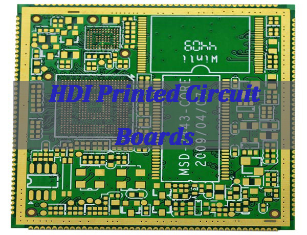
HDI printed circuit boards are advanced PCBs designed for high wiring density and compact electronic systems. They rely on microvia technology, fine-line routing, and multilayer stackups to support complex interconnections within limited board space.
Key characteristics of HDI printed circuit boards include:
High wiring density Enables more signal routing and component placement in smaller board areas.
Microvia technology Uses laser-drilled blind and buried vias, typically ≤ 0.15 mm in diameter, to replace traditional mechanical through-holes.
Fine line width and spacing Supports ultra-fine traces and tight spacing for high-density component layouts.
Advanced multilayer stackups Incorporates sequential lamination and any-layer interconnect structures for greater design flexibility.
Improved signal integrity Shorter interconnect paths and optional low-Dk/Df materials help maintain performance in high-speed designs.
Specialized manufacturing processes Requires precision laser drilling, controlled lamination, and strict process control during the HDI PCB manufacturing process.
In summary, HDI printed circuit boards are not simply denser versions of standard PCBs. They represent a dedicated design and manufacturing approach that enables modern, high-performance electronic products with strict size and performance constraints.
What Makes HDI Circuit Boards Different From Standard Multilayer PCBs?
While both are multilayer structures, HDI PCBs are fundamentally different in their construction and capabilities. Standard multilayer PCBs use mechanical drilling for through-hole vias, which limits density. HDI circuit boards, however, are defined by their use of microvias (typically with a diameter of less than 150µm), which allow for direct interconnections between adjacent layers, unlocking new routing possibilities.
Feature
Standard Multilayer PCB
HDI PCB
Via Technology
Primarily through-hole vias
Microvias, blind/buried vias
Line Width/Space
Larger (e.g., ≥ 4 mil)
Finer (e.g., ≤ 3 mil)
Pad Density
Lower
Much Higher
Construction
Fewer lamination cycles
Multiple sequential laminations
Key Benefit
Cost-effective for simpler designs
Enables miniaturization & high-speed performance
The distinction lies in the high density interconnect approach, which provides superior electrical performance and design freedom, making it ideal for complex, space-constrained applications.
What Is the Structure of HDI Printed Circuit Boards?
The structure of HDI printed circuit boards is not defined by a single, fixed stackup or manufacturing flow. Instead, HDI construction is highly flexible and is determined primarily by via requirements, drilling methods, and interconnection density. The layer structure and production sequence are customized to meet specific routing and component layout demands.
At the core of HDI PCB structure is the combination of multiple via types, each serving a different interconnection purpose:
Laser-drilled blind vias These microvias connect an outer layer to one or more adjacent inner layers. They are a defining feature of HDI printed circuit boards and enable high routing density while minimizing signal path length.
Mechanically drilled buried vias Buried vias connect inner layers without reaching the outer surfaces. They support complex multilayer interconnections and help free surface area for fine-pitch components.
Mechanically drilled through holes Through holes extend from the top layer to the bottom layer and are typically used for power distribution, grounding, or components that require mechanical strength.
Because HDI printed circuit boards often rely on sequential lamination, the final structure may include multiple build-up layers, stacked or staggered microvias, and hybrid via combinations. As a result, each HDI design follows a drilling-driven structural logic, rather than a standardized process template.
In practice, the structure of HDI printed circuit boards is engineered around via architecture, layer interconnect strategy, and manufacturing feasibility, allowing designers to balance density, reliability, and performance in advanced electronic systems.
What Are the Blind Via Types in HDI Printed Circuit Boards?
In HDI printed circuit boards, blind vias are created primarily by laser drilling and are used to connect surface layers to inner layers without penetrating the entire board. Different blind via structures are selected based on layer count, routing density, and reliability requirements.
Common blind via types used in HDI printed circuit boards include:
Microvia hole Typically used in 1+N+1 HDI structures, microvias connect the outer layer to the adjacent inner layer. These vias are laser-drilled and are not copper-filled, making them suitable for simpler HDI designs with moderate density requirements.
Solid via hole (filled microvia) Also applied in 1+N+1 structures, solid vias are laser-drilled microvias that require copper filling. The filled structure provides a flat surface for component pads and supports higher reliability and finer pitch components.
Staggered via hole Used in second-order HDI, staggered vias consist of offset laser-drilled microvias on different layers. This structure reduces stress concentration and is commonly chosen for improved reliability in multilayer HDI designs.
Stacked via hole A key feature of high-density and any-layer HDI, stacked vias are vertically aligned laser-drilled microvias. These vias must be copper-filled to ensure mechanical strength and electrical continuity across multiple layers.
Skip via hole Skip vias are laser-drilled microvias that connect non-adjacent layers, such as from layer 1 directly to layer 3, bypassing layer 2. This structure increases routing flexibility while maintaining surface density.
Step via hole Step vias are co-located second-order laser vias that are not copper-filled. They are typically used in designs where surface planarity is less critical but routing density must still be increased.
How to distinguish blind via structures in HDI designs:
Whether the design is 1+N+1 This indicates the most basic HDI build-up structure, where laser-drilled blind vias connect the outer layers to the adjacent inner layers.
Whether the design is second-order HDI Second-order HDI involves connecting to deeper layers using two sequential microvias, typically requiring either staggered or stacked via structures.
Staggered vs. stacked vias The key distinction is whether the two microvias are vertically aligned.
Staggered vias are offset between layers.
Stacked vias are directly aligned on the same vertical axis.
Filled vs. non-filled vias
Designs using via-in-pad, requiring high surface planarity or higher long-term reliability, typically require copper-filled vias.
Vias that are not located in pads and are used in cost-sensitive designs may remain unfilled, depending on reliability requirements and manufacturing capability.
Each blind via type in HDI printed circuit boards serves a specific structural and electrical function. The selection depends on factors such as layer stackup, component pitch, signal integrity requirements, and manufacturing capability, making blind via design a critical part of HDI PCB engineering.
What Equipment Do HDI Printed Circuit Boards Factories Use for Microvias?
UV or CO₂ Laser Drilling Machines: For ablating precise, small-diameter microvias (as small as 50µm).
Advanced Direct Imaging (DI) Systems: To expose ultra-fine line traces and spaces with high accuracy.
Fully Automated Optical Inspection (AOI): To detect minute defects in traces, spaces, and via pads.
Electroless and Electrolytic Copper Plating Lines: For uniform copper deposition into high-aspect-ratio microvias.
Sequential Lamination Presses: To build the multilayer structure with precise layer-to-layer registration. This specialized toolset is non-negotiable for achieving the yields and quality required in the competitive HDI printed circuit board market.
How to Identify HDI Levels in HDI Printed Circuit Boards?
Identifying the HDI level of HDI printed circuit boards primarily depends on the via structure, rather than on trace etching or basic layer count. While routing processes for multilayer PCBs are largely similar to those used for single- or double-layer boards, the defining difference lies in how vias are formed and interconnected.
At a high level, PCB constructions can be classified into through-hole boards, first-order HDI, second-order HDI, and stacked HDI. Higher-order and any-layer HDI structures exist, but they are used far less frequently due to significantly higher cost and manufacturing complexity.
Through-Hole Boards (Non-HDI)
Through-hole boards use a single via type that runs from the top layer to the bottom layer. All interconnections—both outer and inner—are completed using mechanically drilled through holes that are subsequently copper plated.
The number of layers does not determine whether a board is HDI. A 2-layer PCB is typically a through-hole board, but many high-end products such as network switches or military electronics use 20-layer boards that are still entirely through-hole. Typical finished via diameters range from 0.2 mm to 0.3 mm, with smaller diameters increasing cost due to drill wear and slower drilling speeds.
First-Order HDI (1st-Order HDI)
A first-order HDI board is identified by the presence of one layer of laser-drilled microvias on each outer surface. These microvias usually have diameters around 0.1 mm and connect the outer layers to the adjacent inner layers.
Structurally, a common example is a 6-layer first-order HDI board, which can be viewed as a 4-layer through-hole core with one HDI build-up layer added to each side. The inner layers still rely on mechanical vias, while the outer layers use laser microvias.
Laser drilling only penetrates dielectric material and does not cut through copper, allowing precise via formation without damaging internal circuitry.
Second-Order HDI (2nd-Order HDI)
A second-order HDI board contains two layers of laser-drilled microvias on each side of the core. In practical applications, second-order HDI structures are most commonly found in 8-layer or higher designs, rather than in 6-layer boards.
There are two main second-order configurations:
Staggered vias The two layers of laser microvias are offset from each other. This approach is used because unfilled microvias cannot reliably support another laser via drilled directly on top. Staggered structures reduce process risk and are more cost-effective.
Stacked vias In stacked structures, the laser microvias are vertically aligned. To make this reliable, the lower microvia must be copper-filled before drilling the upper microvia. This process is more complex and significantly more expensive but enables tighter routing density.
In terms of structure:
A 6-layer second-order HDI board can be viewed as a 4-layer first-order board with an additional HDI build-up.
An 8-layer second-order HDI board is effectively a 6-layer first-order board with another build-up layer added.
Any-Layer HDI
Any-layer HDI represents the highest level of HDI technology. Every layer is interconnected using laser-drilled microvias, and any layer can connect directly to any other layer.
This structure offers maximum routing freedom and density, making layout significantly easier for engineers. However, the cost is extremely high—often more than ten times that of a standard through-hole board—so any-layer HDI is reserved for only the most compact and performance-critical designs.
In practice, HDI levels in HDI printed circuit boards are identified by answering three key questions:
Are laser-drilled microvias present? If not, the board is a through-hole design.
How many layers of microvias are used? One layer indicates first-order HDI; two layers indicate second-order HDI.
Are the microvias staggered or stacked? Staggered vias suggest cost-optimized second-order HDI, while stacked vias indicate higher-density, higher-cost designs.
By examining via type, drilling method, and build-up layer count, the HDI level of a printed circuit board can be accurately determined, independent of total layer count alone.
How Does HDI Technology in PCB Improve Signal Integrity?
HDI technology in PCB is a cornerstone for high-speed digital and RF applications because it inherently enhances signal integrity (SI).
Shorter Interconnect Paths: Microvias enable more direct routing, reducing signal path length and propagation delay.
Reduced Parasitics: Smaller via stubs and pads lower parasitic inductance (L) and capacitance (C), minimizing unwanted signal reflection and attenuation.
Better Impedance Control: Finer lines and consistent dielectric layers allow for more precise control over characteristic impedance.
Improved Power Integrity: Dense via-in-pad technology provides low-inductance paths for power delivery networks (PDNs), reducing switching noise.
Enhanced EMI/EMC Performance: Tighter component placement and optimized grounding via microvias help contain electromagnetic interference. These SI benefits make HDI printed circuit boards essential for 5G, high-performance computing, and advanced automotive electronics.
HDI PCB Manufacturing Process Explained Step by Step
In HDI production, the “step-by-step” flow changes with the stackup and via strategy.
Example 1: 1+4+1 (B) Process Flow
(Two lamination cycles, with inner mechanical drilling and plating performed before the second lamination, then laser microvias after the second lamination.)
Panel Cutting
Inner Layer Imaging & Etching
1st Lamination (First Press)
L2–L5 Mechanical Drilling
L2–L5 Copper Plating
L2–L5 Inner/Outer Layer Circuit Formation (for the sub-structure)
2nd Lamination (Second Press)
Laser Drilling (Microvias)
Mechanical Drilling (Through Holes / Tooling Holes as required)
Copper Plating (Via Metallization)
Outer Layer Imaging & Etching
Solder Mask Application
ENIG (Electroless Nickel Immersion Gold)
Legend / Silkscreen Printing
Profiling / Routing (Final Outline)
Electrical Test (E-test)
Final Inspection
OQC (Outgoing Quality Control)
Packing
Warehouse Receiving (Stock-in)
Example 2: 1+4+1 (A) Process Flow
(Single lamination cycle, then laser drilling and standard downstream flow.)
Panel Cutting
Inner Layer Imaging & Etching
Lamination (Pressing)
Laser Drilling (Microvias)
Mechanical Drilling (Through Holes / Tooling Holes as required)
Copper Plating (Via Metallization)
Outer Layer Imaging & Etching
Solder Mask Application
ENIG (Electroless Nickel Immersion Gold)
Legend / Silkscreen Printing
Profiling / Routing (Final Outline)
Electrical Test (E-test)
Final Inspection
OQC (Outgoing Quality Control)
Packing
Warehouse Receiving (Stock-in)
The practical difference between 1+4+1 (A) and 1+4+1 (B) is whether the build requires a staged sequence with an early drill-and-plate step before the second lamination. That staged approach adds process control points and complexity, which often affects lead time and cost.
Example 3: 1+1+8+1+1 Process Flow
Using a 12-layer, double-lamination first-order HDI structure (1+1+8+1+1) as an example, the following briefly outlines the standard manufacturing process commonly used in the industry.
What Applications Use HDI Circuit Boards Most Frequently?
HDI circuit boards are most widely used in applications that demand high signal density, compact form factors, and reliable high-speed performance. As electronic systems continue to evolve toward higher integration and smaller footprints, HDI technology has become a foundational solution across several major industries.
Consumer Electronics and Smartphones
Smartphones remain the largest application segment for HDI circuit boards, accounting for more than half of total HDI demand. Modern smartphone mainboards rely heavily on HDI structures to support high pin-count processors, dense memory interfaces, and multi-antenna RF layouts within extremely limited space.
HDI enables fine line routing, multi-layer interconnects, and compact board stacking, making it essential for slim device profiles and advanced functionality. Wearable electronics further extend this demand, using HDI and embedded via technologies to significantly reduce PCB area.
PC, Consumer Computing, and High-Performance Devices
PCs, tablets, and other consumer computing products represent a rapidly expanding HDI application area. As processors become more powerful and interfaces move toward higher speeds, HDI circuit boards are increasingly adopted to meet routing density and signal integrity requirements.
This segment has grown to roughly one-third of overall HDI demand, driven by compact laptops, high-performance computing modules, and emerging AI-enabled consumer devices.
Automotive Electronics and ADAS Systems
Automotive electronics, particularly ADAS and intelligent vehicle platforms, are a fast-growing HDI application. Vehicle systems require HDI circuit boards to support synchronized multi-sensor signal processing, high-speed data transmission, and stable operation under thermal stress and vibration.
HDI technology enables reliable high-density interconnects for camera modules, radar systems, and in-vehicle infotainment, making it a critical component in the transition toward autonomous and intelligent vehicles.
Communication Infrastructure and 5G Equipment
HDI circuit boards are widely used in 5G base stations and communication equipment, where high-frequency, low-loss signal transmission is essential. These systems require fine-line HDI layouts to support large antenna arrays, RF front-end integration, and high-speed signal processing.
The increasing complexity of 5G infrastructure continues to push higher layer counts and tighter precision requirements, accelerating HDI adoption in telecom applications.
Medical Electronics and Healthcare Devices
Medical electronics represent a smaller but high-value HDI segment. Advanced imaging systems, implantable medical devices, and portable diagnostic equipment rely on HDI circuit boards to achieve miniaturization, high reliability, and precise signal acquisition.
HDI flexible and rigid-flex structures are particularly important in medical applications where space constraints and signal accuracy are critical.
AI Servers and Emerging High-Growth Segments
AI servers and data-center hardware are emerging as one of the fastest-growing HDI application areas. The need for ultra-high interconnect density, high-speed signal integrity, and multilayer routing has made HDI circuit boards a key enabler for advanced computing platforms.
As AI workloads and server architectures continue to evolve, higher-order HDI and any-layer HDI solutions are increasingly replacing traditional PCB designs.
In summary, HDI circuit boards are most frequently used in:
Smartphones and consumer electronics
PCs, tablets, and high-performance consumer devices
Automotive electronics and ADAS systems
5G communication infrastructure
Medical and healthcare electronics
AI servers and advanced computing hardware
Across these applications, HDI technology plays a central role in enabling miniaturization, high-speed performance, and system-level integration, making it one of the most important PCB technologies in modern electronics manufacturing.
What Capabilities Should You Expect From an HDI PCB Manufacturer?
When selecting an HDI PCB manufacturer, particularly one claiming full turnkey capability, it’s crucial to understand the specific advanced technological competencies they must possess. A true specialist in high density interconnect must demonstrate proficiency far beyond standard PCB fabrication. Based on our internal process capabilities at BEST Technology, here are the definitive capabilities you should expect from a leading HDI PCB manufacturer.
An advanced HDI printed circuit board supplier must be able to deliver on the following key areas to ensure your HDI printed circuit boards meet the highest standards of performance, miniaturization, and reliability:
Laser Drilling Mastery: The capability to consistently drill microvias with diameters down to 0.070mm (limit) or 0.10mm (standard), a fundamental requirement for what is HDI PCB. This includes controlling the depth-to-diameter ratio precisely.
Complex Lamination Expertise: Proficiency in executing multi-stage sequential lamination processes (1+N+1, 2+N+2, etc.) with exceptional layer-to-layer registration (alignment tolerance ≤0.13mm standard, ≤0.10mm limit). This is critical for building reliable any-layer HDI printed circuit boards.
Ultra-Fine Line & Space Imaging:
Sub-4mil Resolution: The ability to reliably manufacture extremely fine traces and spaces. For outer layers, this means achieving 3.5/4mil (standard) or even 3/3mil (limit). On inner layers, capabilities extend to 3/3mil (standard) or 2.5/2.5mil (limit), which is essential for high density PCB designs requiring maximum component density.
Controlled Etching: Maintaining tight etch tolerances (e.g., ±1mil for lines ≤5mil) to ensure geometric accuracy and consistency.
Advanced Impedance Control:
Dielectric Management: Precise control over insulation layer thickness (minimum 0.076mm standard) and material properties to achieve consistent electrical characteristics.
Targeted Impedance Performance: Delivering specified impedance values (e.g., 50Ω, 100Ω differential) with tight tolerances (±5Ω for <50Ω impedance, standard), which is vital for maintaining signal integrity in high-speed HDI technology in PCB applications.
Broad Material & Surface Finish Portfolio:
High-Performance Substrates: Access to and proven experience with a wide variety of materials, including standard FR4 (normal, medium, and high TG), high CTI materials, and specialized high-frequency/low-loss laminates (e.g., Rogers, Taconic series), catering to demanding applications in the HDI printed circuit board market.
Diverse Surface Treatments: Offering a comprehensive range of surface finishes such as ENIG, Immersion Tin/Silver, OSP, Hard/Soft Gold, and ENEPIG to meet various assembly requirements and component specifications.
Integrated Full-Turnkey Services:
Proactive Design Support (DFM): Providing expert engineering feedback during the design phase to optimize for manufacturability, performance, and HDI printed circuit boards price considerations.
Seamless Fabrication-to-Assembly Flow: Managing the entire process under one roof, from HDI PCB manufacturing process execution to precision SMT/BGA assembly, ensuring quality, traceability, and faster time-to-market.
Rigorous Testing & Validation: Implementing thorough testing protocols, including electrical testing (flying probe, ICT), AOI, and functional testing, to guarantee the reliability of complex HDI assemblies.
In summary, a premier HDI printed circuit board supplier with full turnkey capability integrates these sophisticated technologies and services. BEST Technology’s detailed process capabilities, as reflected in our manufacturing specifications, underscore our commitment to delivering the highest quality HDI printed circuit boards for the most challenging applications. We possess the advanced infrastructure, technical expertise, and integrated services necessary to transform your complex HDI designs into successful, high-performance products.
How to Choose a Reliable HDI Printed Circuit Board Supplier?
Choosing the right HDI printed circuit board supplier is a strategic decision. Follow this checklist:
Audit Technical Certifications: Look for ISO 9001, IATF 16949 (automotive), and relevant industry-specific certifications.
Review Their Portfolio: Examine case studies or samples of similar complexity (HDI level, layer count, material).
Evaluate Communication: Assess their responsiveness, engineering support, and willingness to provide HDI printed circuit boards quotes with clear breakdowns.
Request a Facility Tour/Virtual Audit: Verify their equipment (laser drillers, DI machines) and process controls.
Check Supply Chain Stability: Ensure they have strong relationships with material suppliers to mitigate shortage risks.
Discuss Prototype & Volume Scalability: Confirm they can support both rapid prototyping and volume production. Thorough vetting separates true technical partners from basic board vendors.
HDI Printed Circuit Boards Price Factors and Cost Considerations
The HDI printed circuit boards price is influenced by multiple, often interrelated, factors. Understanding them helps in budget planning and design optimization.
Layer Count & Board Size: More layers and custom sizes use more material and process time.
Material Type: Standard FR-4 vs. high-speed/low-loss or halogen-free materials.
Minimum Feature Size: Tighter trace/space and smaller microvia diameters require more precise (and expensive) processes.
Surface Finish: ENIG, ENEPIG, or hard gold are costlier than HASL.
Quantity & Lead Time: Prototype quantities have higher unit costs; expedited turnarounds incur premiums. A trusted manufacturer will work with you to find the most cost-effective design path without compromising critical performance.
How Is the HDI Printed Circuit Board Market Evolving With AI and 5G?
The HDI printed circuit board market is undergoing a fundamental transformation, shifting from a cycle driven primarily by consumer electronics miniaturization to one powered by the high-performance demands of artificial intelligence (AI) and ubiquitous 5G connectivity. This evolution is not merely a growth in volume but a strategic upgrade in technology, value, and application focus, creating new high-growth segments and reshaping competitive dynamics.
1. Market Overview: From 5G Build-out to an AI-Powered Future
The market trajectory clearly illustrates this shift. In 2023, the global HDI board market, valued at approximately 8.5 billion with China accounting for4210 billion, growing at a rate of 9.2%, primarily fueled by AI servers and automotive electronics. This is moving the industry’s focus from volume to advanced capability, as seen in the rising proportion of Any-layer HDI, projected to reach 28% by 2025.
2. Primary Growth Drivers: A Confluence of Megatrends
The demand surge is coming from multiple, synergistic frontiers:
AI Server Demand Explosion: This is the most potent driver. AI training chips (e.g., NVIDIA H100) require HDI boards with 20+ layers, with per-unit value reaching 3-5 times that of traditional servers. The global market for HDI in AI servers is forecast to surpass $2.5 billion by 2025. This creates intense demand for boards that support heterogeneous integration technologies like 2.5D/3D packaging and can manage thermal loads from chips consuming over 1000W.
Automotive Electronics Penetration: Advanced Driver-Assistance Systems (ADAS) and smart cockpits are drastically increasing HDI content per vehicle from 1-2 pieces to 5-8 pieces. The automotive segment’s share of the HDI market is expected to rise from 15% to 25% by 2025, demanding ultra-high reliability.
Accelerated 5G & Data Center Infrastructure: The rollout of Massive MIMO antennas and the upgrade to 800G optical modules in data centers require high-frequency, high-speed HDI boards with extremely fine line widths/spaces (below 20µm) and ultra-low signal loss, pushing the limits of manufacturing processes like mSAP.
3. Application Shift: Beyond the Smartphone Core
While smartphones remain the dominant application, accounting for 58% of demand, the future growth engine is demonstrably elsewhere. The combined share of PC/consumer electronics (30%) and automotive electronics (7%) highlights HDI’s expanding role in computing and automotive intelligence. The 42% non-smartphone segment represents a vast technology substitution space, where high-end HDI is progressively replacing traditional PCBs, a process that will continue to deepen.
4. Technological and Supply Chain Transformation
The requirements of AI and 5G are forcing a comprehensive upgrade across the HDI PCB manufacturing ecosystem:
Technology Trends: Line/space is advancing toward 30/30µm, and the penetration of SLP (Substrate-Like PCB) technology is increasing.
New Capabilities Required: Manufacturers must master advanced thermal management (embedded copper blocks, metal cores), supply ultra-low-loss materials for high-frequency applications, and build full turnkey capabilities—from collaborative design and simulation to full-scale production and testing—to meet the stringent demands of clients like NVIDIA.
In summary, the HDI printed circuit board market is decisively evolving from enabling device miniaturization to becoming the critical backbone of the AI and 5G infrastructure. Growth is being driven by high-value, high-complexity applications in AI servers, autonomous vehicles, and advanced communications, which in turn are triggering a wave of technological innovation and supply chain restructuring. Manufacturers that can master advanced processes like Any-layer HDI, ultra-fine line imaging, and integrated thermal management, while providing comprehensive full turnkey solutions, are positioned to lead the next phase of the industry’s evolution.
In conclusion, HDI printed circuit boards are the foundational technology enabling the miniaturization, high speed, and reliability of today’s most advanced electronic devices. This guide has explored their design, manufacturing, applications, and the critical factors in selecting a manufacturing partner. Success in this complex domain hinges on collaboration with a supplier that offers genuine full turnkey capability—seamlessly integrating design support, advanced fabrication, precise assembly, and rigorous testing under one roof. BEST Technology is committed to being that partner, providing the expertise and end-to-end service to bring your most ambitious HDI projects to life with efficiency. For a consultation or quote, please contact us at sales@bestpcbs.com.
FAQs
What Are the Benefits of HDI PCB?
HDI PCBs offer significantly higher wiring density compared to traditional multilayer boards. By using microvias, fine line/space routing, and build-up layers, HDI technology enables smaller board size, lighter weight, and higher component integration. HDI PCBs also improve signal integrity by shortening interconnect paths and reducing parasitic effects, making them well suited for high-speed and high-frequency designs.
What Is Ultra HDI PCB?
Ultra HDI PCB refers to advanced, high-order HDI designs that go beyond standard first- or second-order HDI. These boards typically feature ultra-fine line widths, very small laser microvias, multiple build-up layers, and in many cases stacked or any-layer interconnect structures. Ultra HDI is commonly used in smartphones, AI hardware, and other applications where extreme miniaturization and routing density are required.
What Are the Four Tiers of HDI?
The four tiers of HDI are usually classified by the number of build-up layers and microvia levels:
Tier 1 (First-Order HDI) – One layer of laser microvias on each side of the core (e.g., 1+N+1).
Tier 2 (Second-Order HDI) – Two layers of microvias, using staggered or stacked via structures.
Tier 3 (Higher-Order HDI) – Three or more microvia layers, supporting much higher routing density.
Tier 4 (Any-Layer HDI) – Every layer can be interconnected with laser microvias, offering maximum design flexibility at the highest cost.
What Does 1 HDI Mean?
“1 HDI” typically means a first-order HDI PCB, which uses one build-up layer of laser-drilled microvias on each side of the core. This structure is commonly expressed as 1+N+1 and represents the entry level of HDI technology, balancing higher density with controlled manufacturing cost.
This website uses cookies to enhance your experience, remember your preferences, and help us understand how visitors use our site. You can accept all cookies, reject non-essential cookies, or manage your settings.
This website uses cookies to improve your experience while you navigate through the website. Out of these cookies, the cookies that are categorized as necessary are stored on your browser as they are essential for the working of basic functionalities of the website. We also use third-party cookies that help us analyze and understand how you use this website. These cookies will be stored in your browser only with your consent. You also have the option to opt-out of these cookies. But opting out of some of these cookies may have an effect on your browsing experience.
Necessary cookies are absolutely essential for the website to function properly. These cookies ensure basic functionalities and security features of the website, anonymously.
Cookie
Duration
Description
cookielawinfo-checkbox-analytics
11 months
This cookie is set by GDPR Cookie Consent plugin. The cookie is used to store the user consent for the cookies in the category "Analytics".
cookielawinfo-checkbox-functional
11 months
The cookie is set by GDPR cookie consent to record the user consent for the cookies in the category "Functional".
cookielawinfo-checkbox-necessary
11 months
This cookie is set by GDPR Cookie Consent plugin. The cookies is used to store the user consent for the cookies in the category "Necessary".
cookielawinfo-checkbox-others
11 months
This cookie is set by GDPR Cookie Consent plugin. The cookie is used to store the user consent for the cookies in the category "Other.
cookielawinfo-checkbox-performance
11 months
This cookie is set by GDPR Cookie Consent plugin. The cookie is used to store the user consent for the cookies in the category "Performance".
viewed_cookie_policy
11 months
The cookie is set by the GDPR Cookie Consent plugin and is used to store whether or not user has consented to the use of cookies. It does not store any personal data.
Functional cookies help to perform certain functionalities like sharing the content of the website on social media platforms, collect feedbacks, and other third-party features.
Performance cookies are used to understand and analyze the key performance indexes of the website which helps in delivering a better user experience for the visitors.
Analytical cookies are used to understand how visitors interact with the website. These cookies help provide information on metrics the number of visitors, bounce rate, traffic source, etc.
Advertisement cookies are used to provide visitors with relevant ads and marketing campaigns. These cookies track visitors across websites and collect information to provide customized ads.