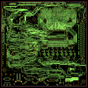
A 20 layer PCB is usually chosen when a design needs more routing channels, reference planes, or power distribution than a lower-layer board can comfortably provide. High-pin-count BGAs, fast digital interfaces, multiple voltage rails, limited board area, and strict EMI requirements are common reasons to move toward this type of construction. The extra layers offer more design freedom, but they also make stackup planning, drilling, lamination, and registration more demanding.
EBest Circuit manufactures multilayer PCBs and supports engineering review for stackup, controlled impedance, via structures, materials, and DFM. If your design is already at the 16- to 20-layer stage, sending the Gerber or ODB++ data together with target thickness, copper weight, impedance requirements, and drill information allows the board construction to be reviewed before quotation or prototype release.

What Is a 20 Layer PCB?
A 20 layer PCB uses twenty copper layers to combine dense routing, reference planes, power distribution, and controlled-impedance structures in one multilayer board. It is appropriate only when the design needs the extra routing and plane flexibility.
A practical stackup normally combines:
A 20 layer board should be selected from routing, power, EMI, and mechanical requirements rather than layer count alone.
- Signal layers for component breakout and routing
- Ground planes for return paths and shielding
- Power planes for voltage distribution
- Reference planes for controlled-impedance signals
The advantage is not simply “more layers.” What matters is how those layers are allocated. A good 20-layer construction can give high-speed traces nearby reference planes, keep return paths continuous, and provide enough routing space without pushing trace width and spacing unnecessarily tight.
When Do You Need a 20 Layer PCB?
A 20-layer structure makes sense when a lower layer count starts forcing electrical or routing compromises.
Typical cases include:
- High-pin-count BGA, CPU, FPGA, or ASIC breakout
- Multiple DDR, PCIe, Ethernet, SerDes, USB, or other high-speed interfaces
- Several power rails requiring dedicated plane area
- Dense layouts where board size cannot increase
- Mixed analog, digital, RF, and power circuitry
- Designs requiring additional ground planes for EMI control
- Backplanes, servers, telecom equipment, medical electronics, aerospace systems, and complex industrial controls
More layers are not automatically better. If a 16-layer board already meets routing, signal-integrity, power-integrity, and mechanical requirements with reasonable margin, moving to 20 layers only adds fabrication complexity and cost.
What Does a Typical 20 Layer PCB Stackup Look Like?
There is no universal 20 layer PCB stackup. Layer allocation depends on BGA escape, impedance requirements, dielectric thickness, copper weight, power distribution, and the intended via structure.
This pcb layer stack up example is illustrative; the production construction must be recalculated for the approved materials and impedance targets. See our PCB board stackup guide.
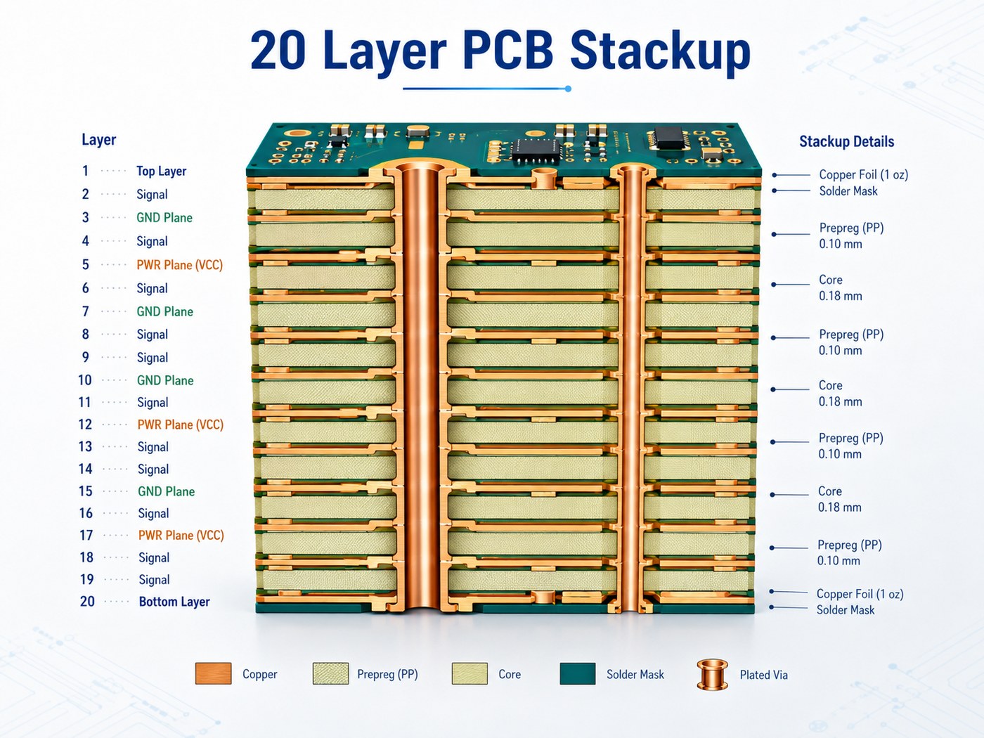
A possible 20 layer PCB stackup example is shown below.
| Layer | Type | Typical Function |
| L1 | Signal | Components and short routing |
| L2 | Ground | Reference plane |
| L3 | Signal | High-speed routing |
| L4 | Ground | Reference plane |
| L5 | Signal | General routing |
| L6 | Power | Power distribution |
| L7 | Signal | General/high-speed routing |
| L8 | Ground | Reference plane |
| L9 | Signal | High-speed routing |
| L10 | Ground | Central reference plane |
| L11 | Ground | Central reference plane |
| L12 | Signal | High-speed routing |
| L13 | Ground | Reference plane |
| L14 | Signal | General/high-speed routing |
| L15 | Power | Power distribution |
| L16 | Signal | General routing |
| L17 | Ground | Reference plane |
| L18 | Signal | High-speed routing |
| L19 | Ground | Reference plane |
| L20 | Signal | Components and routing |
This is an example, not a standard construction. A real project may need more power layers, fewer signal layers, different dielectric spacing, or another reference-plane arrangement. The stackup should be finalized against the actual impedance and manufacturing requirements rather than copied from another PCB.
How Should Signal, Ground, and Power Layers Be Arranged?
Layer placement should give critical signals a stable reference and keep the overall construction reasonably symmetrical.
Several rules are especially useful:
- Place high-speed signal layers next to continuous ground planes.
- Avoid routing critical traces across gaps or splits in their reference plane.
- Use ground layers between sensitive or unrelated routing regions when isolation is important.
- Keep power and ground planes appropriately coupled where the stackup allows.
- Maintain a reasonably symmetrical dielectric and copper structure around the board center.
- Avoid large copper-density differences between opposite sides of the stack.
Return-path planning is particularly important. When a high-speed signal changes layers, the return current must also transition between reference planes. If both references are ground, nearby stitching vias can provide a short return path.
Layer assignment is best decided before detailed routing. Changing the stackup late in the design can alter impedance geometry and force trace-width or spacing changes.
What Is the Typical 20 Layer PCB Thickness?
There is no single standard 20 layer PCB thickness. The finished value comes from the complete copper and dielectric build rather than the layer count by itself.
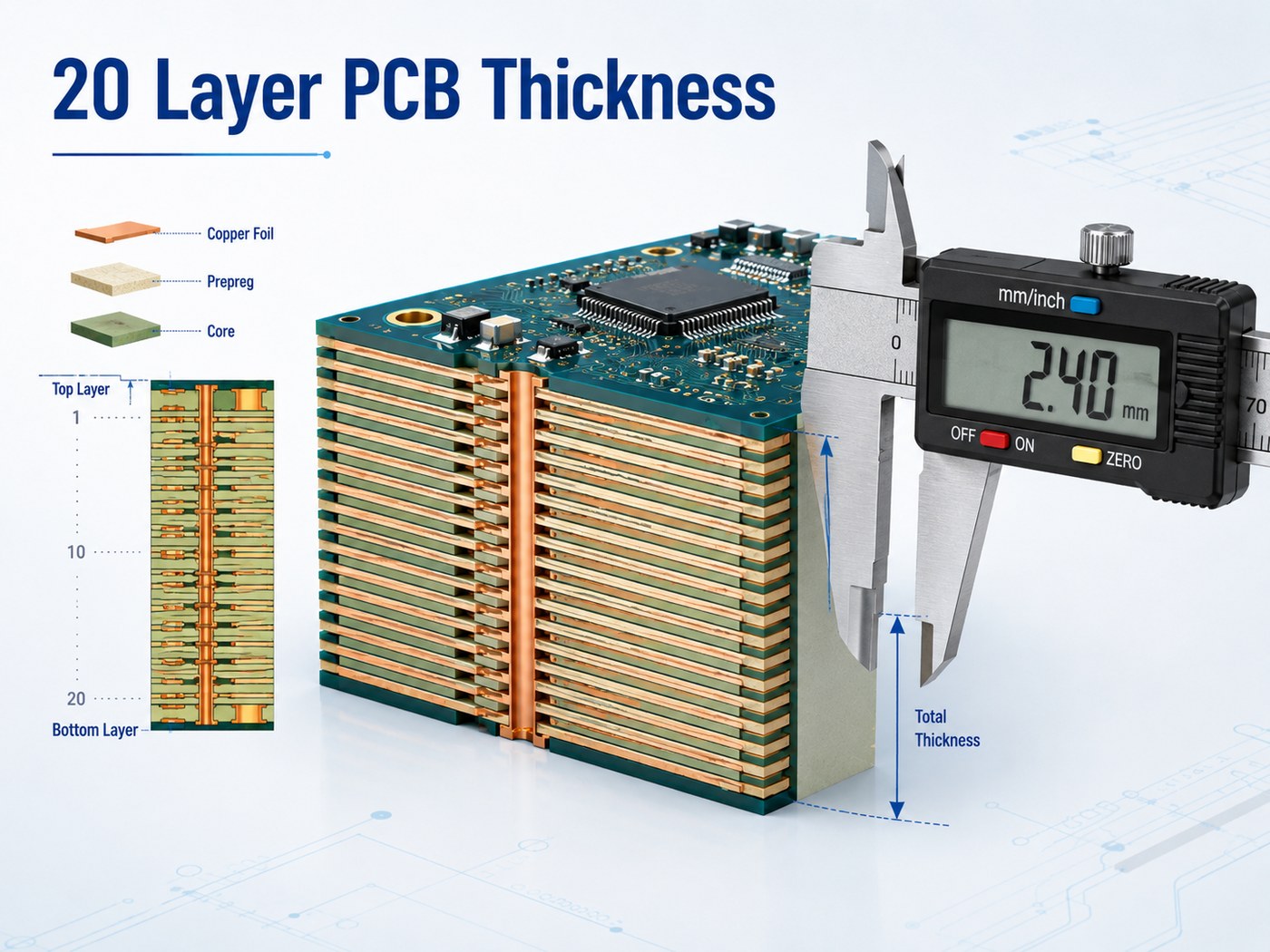
Finished thickness is mainly determined by:
- Core thickness
- Cured prepreg thickness
- Copper weight
- Required finished copper
- Controlled-impedance geometry
- Electrical isolation requirements
- Via diameter and drill aspect ratio
- Connector and enclosure requirements
- Mechanical stiffness
Trying to make a 20-layer board unusually thin means using thinner dielectric layers. That can affect impedance geometry, laminate availability, registration tolerance, and mechanical strength.
Board thickness also needs to be reviewed with the drill table. A thick PCB combined with very small mechanically drilled holes can create an aggressive aspect ratio, making hole preparation and plating more difficult. For this reason, thickness, stackup, impedance, and hole structure should be evaluated together.
Which Materials Are Used for 20 Layer PCBs?
Layer count alone does not determine the laminate. Material selection should follow the electrical, thermal, reliability, and cost requirements.
Our PCB material guide explains how Tg, loss, and laminate construction affect selection.
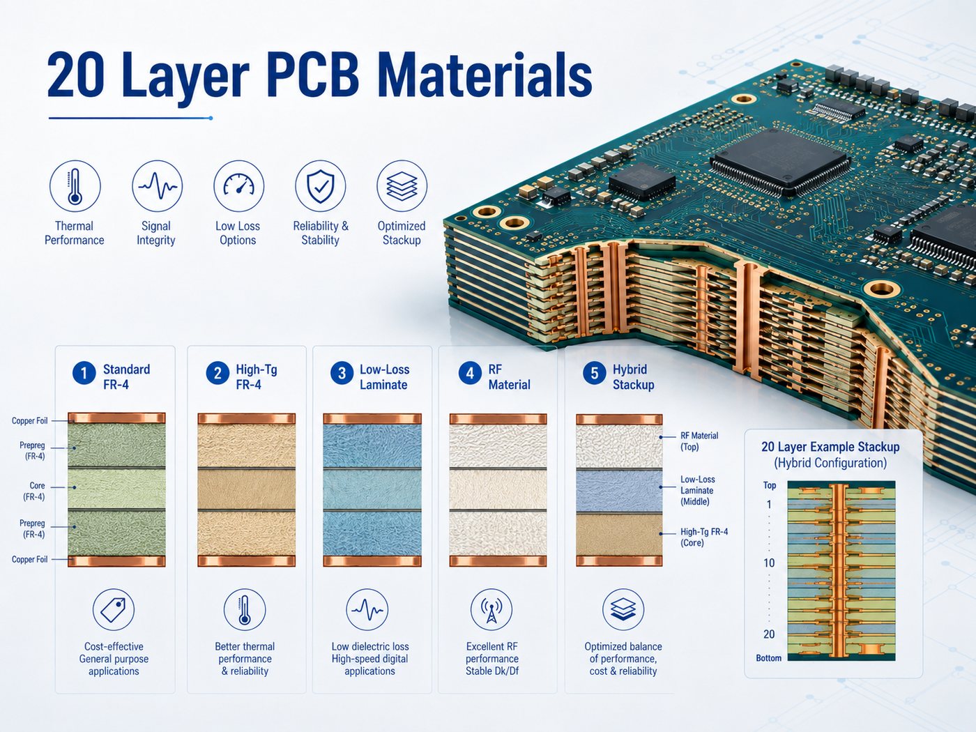
| Material Type | Typical Use | Main Consideration |
| Standard FR-4 | General industrial electronics | Economical for less demanding signal speeds |
| High-Tg FR-4 | Dense boards with higher thermal demands | Better thermal robustness |
| Low-loss laminate | High-speed digital systems | Lower transmission loss |
| RF/high-frequency laminate | RF and microwave sections | More stable Dk and lower Df |
| Hybrid stackup | Mixed digital/RF designs | Lamination compatibility needs review |
For high-speed boards, two material properties deserve particular attention:
- Dk influences impedance and propagation delay.
- Df contributes to dielectric loss, especially as frequency and trace length increase.
Availability also matters. A laminate may look ideal electrically but become impractical if the required core or prepreg thickness is difficult to source for prototypes or volume production. Hybrid constructions need closer review because different material systems may have different resin behavior, CTE, and lamination conditions.
How Do You Design a 20 Layer PCB for Signal and Power Integrity?
More layers make SI and PI design easier only when they are used correctly.
For manufacturing controls, review our impedance control PCB guide.
For controlled impedance, the PCB manufacturer needs more than the requested value. Actual impedance depends on:
- Trace width
- Copper thickness
- Dielectric thickness
- Dk
- Distance to the reference plane
- Differential-pair spacing
- Manufacturing tolerance
The production impedance calculation should therefore use the actual fabrication stackup rather than nominal CAD dimensions alone.
Other practical design points include:
- Keep high-speed traces over continuous reference planes.
- Avoid unnecessary layer changes on sensitive interfaces.
- Add suitable return-path vias when reference planes change.
- Control coupling between neighboring high-speed routes.
- Review via stubs on faster channels.
- Keep decoupling paths short between the power pin, capacitor, and ground.
- Allocate sufficient copper for major power rails.
Via stubs can become important at higher data rates. If a through via continues well beyond the layers carrying the signal, the unused section acts as a stub. Back drilling or a shorter blind-via transition may be considered when channel analysis shows the stub is significant.
The objective is not to fill the stackup with ground and power planes. It is to create enough routing space while maintaining clean reference paths and a low-impedance power-distribution network.
Which Via Structures Are Suitable for a 20 Layer PCB?
A 20 layer PCB does not automatically need HDI construction. The appropriate via type depends mainly on package pitch, routing density, board thickness, and the layers that must be connected.
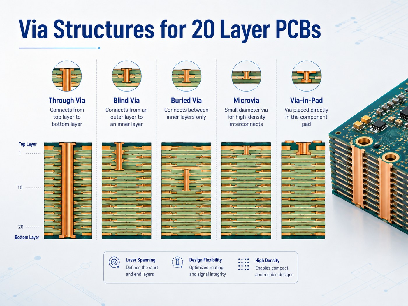
| Via Type | Suitable Situation | Main Trade-Off |
| Through via | Moderate routing density | Occupies space through the full stack |
| Blind via | Dense outer-layer breakout | More process steps |
| Buried via | Internal layer connections | More complex lamination |
| Microvia | Fine-pitch BGA or HDI routing | Often requires sequential lamination |
| Via-in-pad | Very dense BGA escape | Filling and planarization usually required |
| Staggered microvia | Multi-level HDI routing | More layout planning |
| Stacked microvia | Vertical HDI interconnect | Tighter process and reliability control |
For example, a 20-layer industrial controller with generous component pitch may work well with conventional through vias. A much smaller board using fine-pitch BGAs may require microvias even at the same layer count.
Layer count and HDI level are separate design decisions.
How Is a 20 Layer PCB Manufactured?
The basic process is similar to other multilayer PCBs, but dimensional control becomes more important as the stack grows.
A typical manufacturing flow includes:
- Inner-layer imaging and etching
- Inner-layer AOI
- Surface preparation
- Core and prepreg layup
- Multilayer lamination
- Mechanical or laser drilling
- Hole metallization and copper plating
- Outer-layer imaging and etching
- Solder mask
- Surface finish
- Electrical testing
- Final inspection
A conventional through-hole board may use one main multilayer lamination cycle. Designs with buried vias or multi-level microvias can require repeated lamination, drilling, and plating.
That difference can have a major effect on cost and lead time. A “20-layer PCB” therefore tells the manufacturer much less than a complete stackup and via diagram.
What Are the Key Manufacturing Challenges of a 20 Layer PCB?
The main challenge is controlling many interacting tolerances at the same time.
Important DFM points include:
- Layer registration: inner layers can expand or contract during processing, so registration compensation is required.
- Drill aspect ratio: small holes through a thick board are more difficult to prepare and plate reliably.
- Resin flow: uneven copper distribution can affect dielectric thickness and resin fill.
- Copper balance: severe imbalance may contribute to bow and twist.
- Hole-wall plating: plating must remain continuous through the full hole depth.
- CAF risk: conductor and hole spacing, material selection, and process control deserve attention on dense multilayer designs.
- Delamination: laminate condition, moisture control, pressing, and thermal exposure all matter.
- Impedance consistency: dielectric and copper tolerances need to stay within the range used for the impedance calculation.
A useful DFM review should therefore examine the real stackup, drill map, copper distribution, via construction, impedance table, and material specification—not just confirm that the factory can produce “20 layers.”
20 Layer PCB vs 16 Layer PCB: Which Should You Choose?
A 20-layer board provides more routing and plane-allocation freedom, while a 16-layer structure is generally simpler to manufacture.
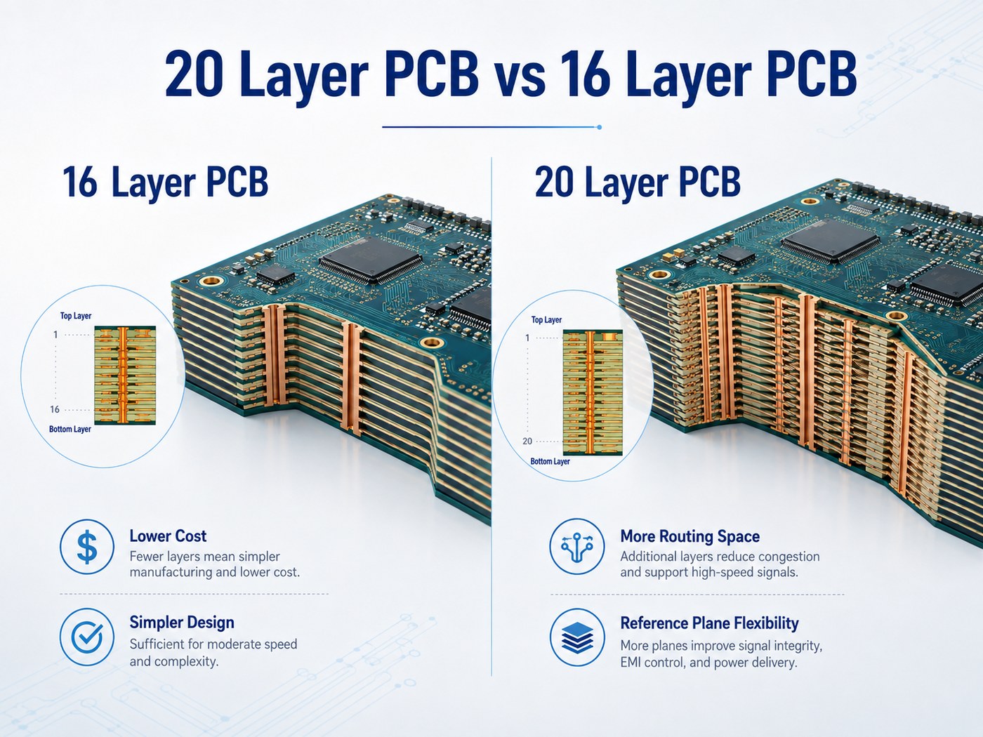
| Factor | 16 Layer PCB | 20 Layer PCB |
| Routing capacity | High | Higher |
| Reference-plane flexibility | Good | Greater |
| Power-plane allocation | Good | More flexible |
| Dense BGA routing | Suitable for many designs | Better for highly congested designs |
| Stackup complexity | Lower | Higher |
| Fabrication cost | Lower | Higher |
| Manufacturing difficulty | Lower | Higher |
Consider moving from 16 to 20 layers when the 16-layer design causes:
- Excessive routing congestion
- Too many signal layer transitions
- Broken or compromised reference planes
- Inadequate BGA escape channels
- Insufficient room for power planes
- Trace spacing that is unnecessarily aggressive
If those problems do not exist, 16 layers may be the more economical choice.
What Affects 20 Layer PCB Cost and Lead Time?
Layer count matters, but two 20-layer designs can still have very different prices.
The largest quotation variables usually include:
- Board dimensions and panel utilization
- Laminate type and availability
- Finished thickness
- Copper weight
- Minimum trace and spacing
- Minimum finished hole size
- Blind, buried, or microvia structures
- Number of sequential lamination cycles
- Via filling or via-in-pad
- Controlled impedance
- Back drilling
- Surface finish
- Testing requirements
- Prototype or production quantity
A conventional FR-4 board using through vias is generally less complex than a 20-layer low-loss design with stacked microvias, back drilling, via filling, and tight impedance requirements.
For a meaningful quotation, provide the complete fabrication requirements rather than asking for a generic “20 layer PCB price.”
20 Layer PCB FAQ
How thick is a 20 layer PCB?
There is no fixed thickness. It depends on the core and prepreg structure, copper weight, controlled-impedance geometry, via structure, and mechanical requirements. If the finished thickness is mechanically constrained, specify it early so the stackup and drill aspect ratio can be evaluated together.
How many signal layers does a 20 layer PCB have?
There is no standard number. Some 20-layer boards may use around half of the layers for routing, while others allocate more copper layers to ground or power. The correct ratio depends on routing density, power distribution, and signal-integrity requirements.
Does a 20 layer PCB always require HDI technology?
No. A conventional through-hole construction can be suitable when component pitch and routing density allow it. HDI becomes useful when fine-pitch BGA breakout or limited PCB area requires blind vias, buried vias, or microvias.
Can a 20 layer PCB use standard FR-4?
Yes, when its loss, thermal, and reliability requirements are compatible with standard FR-4. High-speed interfaces, long transmission paths, or higher thermal demands may justify high-Tg or lower-loss laminates.
What files are required for a 20 layer PCB quote?
For an accurate review and quotation, provide as much of the following as available:
- Gerber or ODB++ files
- NC drill files
- Fabrication drawing
- Finished board thickness
- Copper weight
- Existing stackup
- Controlled-impedance requirements
- Via structure
- Material preference
- Surface finish
- Quantity
- Inspection or reliability requirements
A 20 layer PCB is most useful when the added layers solve real routing, reference-plane, power-distribution, or density problems. Stackup, thickness, material, impedance, and via architecture should be developed as one system rather than specified independently.
How Can EBest Circuit Support Your 20 Layer PCB Project?
A supplier’s published maximum layer count is only a starting point. What matters is whether its process capability matches your actual stackup.
Check whether the manufacturer can support:
- Multilayer stackup engineering
- Controlled-impedance calculation and verification
- Required minimum trace, spacing, and hole geometry
- Blind and buried vias
- HDI and sequential lamination where required
- Via filling and via-in-pad
- Inner-layer AOI
- Electrical testing
- Cross-section inspection where needed
- Material and production traceability
- Relevant quality-system requirements
- DFM review before fabrication
Engineering communication is also revealing. If a stackup, drill structure, or impedance requirement is unclear, the issue should be raised before production rather than interpreted silently.
For EBest Circuit projects, customers can provide Gerber or ODB++, drill files, fabrication notes, target thickness, impedance information, and material requirements for engineering review before prototype or volume production.
Send us your Gerber or ODB++ files, drill data, target thickness, material grade, copper weights, impedance targets, via structure, quantities, and test requirements. We can review stackup balance and manufacturability before quotation and prototype release.