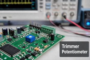
A digital potentiometer adjusts resistance through an electronic command instead of a mechanical knob. It is often used for calibration, gain control, sensor trimming, display adjustment, and other settings that need to be changed by a microcontroller.
Choosing one for a PCB involves more than selecting a resistance value. The device must work with the circuit voltage, provide the right resolution, behave correctly when power is turned on, and fit the approved PCB footprint. The assembled board also needs a functional test that confirms the output changes as intended.
This guide explains the information engineers and buyers should check when selecting a digital potentiometer and preparing a board for PCB assembly.
What Is a Digital Potentiometer and How Does It Work?
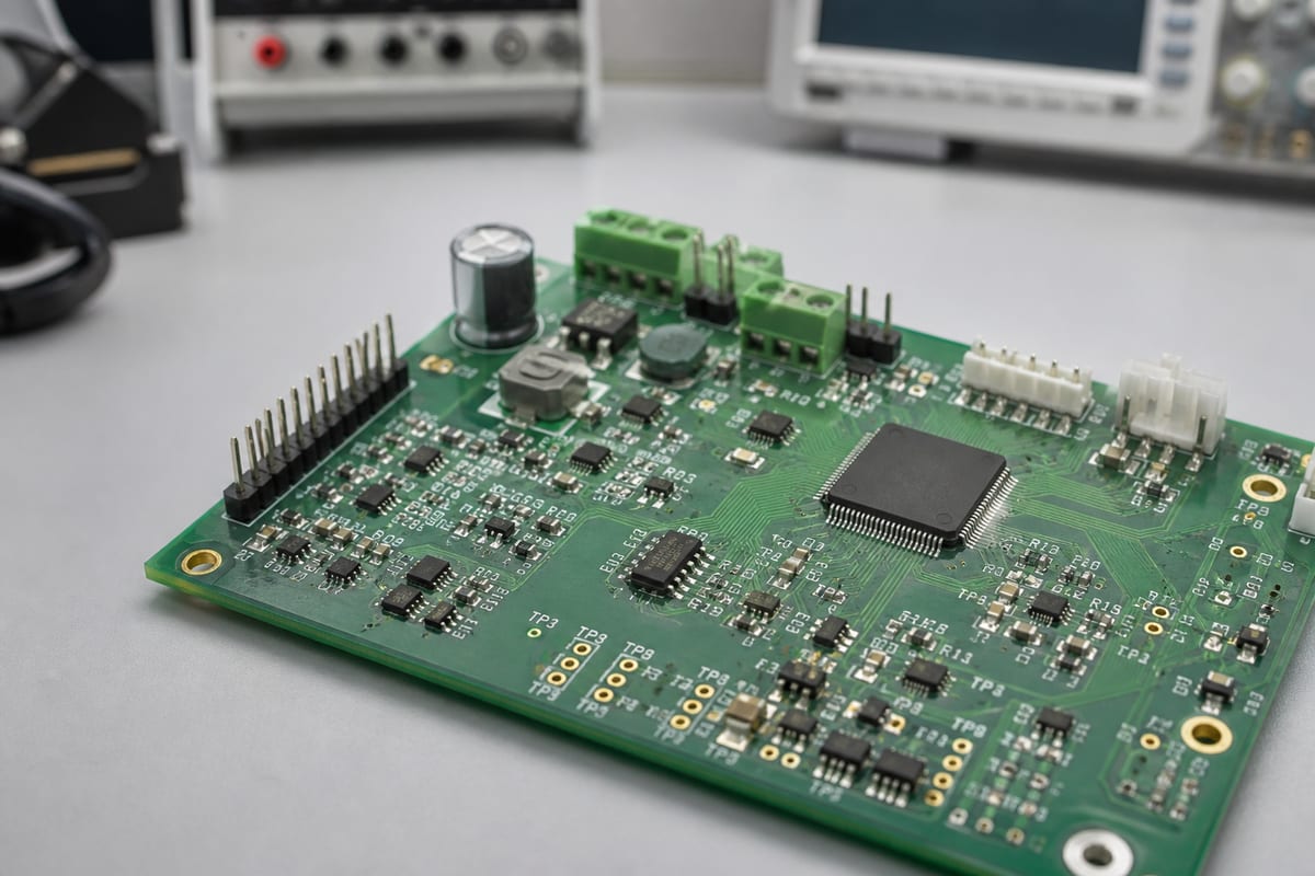
A digital potentiometer, often called a digipot, contains a resistor string and an electronically controlled wiper. A microcontroller changes the wiper position through SPI, I2C, up/down pins, or, in some products, pushbuttons.
The high, low, and wiper terminals resemble the three terminals of a mechanical potentiometer, but they cannot always be used in the same way. They are semiconductor connections with limits on voltage, current, and power. Some devices allow signals only between their supply rails, while others support a wider terminal range. The exact datasheet must be checked before the part is placed in the circuit.
The main specifications include:
- End-to-end resistance and tolerance
- Number of taps and step size
- Linear or logarithmic adjustment
- Wiper resistance and current limit
- SPI, I2C, or up/down control
- Volatile or nonvolatile memory
- Power-on wiper position
- Package, pinout, and temperature grade
Use the complete manufacturer part number in the BOM. Parts in the same family may have different resistance values, memory options, interfaces, or packages, even when their abbreviated descriptions look similar.
Digital Potentiometer vs Analog Potentiometer for PCB Design
A mechanical potentiometer keeps its physical wiper position when power is removed. A digital potentiometer may return to a default value or recall a stored setting, depending on the device. This difference can affect how the product behaves during startup.
| Design question | Digital potentiometer | Mechanical potentiometer | What to check |
|---|---|---|---|
| How is it adjusted? | Firmware or digital input | Knob, slider, or trimmer | Who needs to change the setting? |
| What happens at power-up? | Default or stored code | Wiper stays in position | Is the initial output safe? |
| What signal can it handle? | Limited by IC ratings | Limited by track and contact ratings | Check actual voltage and current |
| How is it mounted? | Small IC package | Mechanical body and mounting hardware | Check PCB and enclosure space |
| How is it tested? | Send a command and measure the output | Move the wiper and measure the output | Define the expected result |
A digipot is useful when the setting must be controlled remotely, repeated accurately, saved in memory, or adjusted during automatic calibration. A mechanical potentiometer may be better when the circuit must work without power, the user needs direct manual control, or the signal exceeds the ratings of available digital devices.
How to Choose a Digital Variable Resistor
Start with the circuit rather than a distributor search filter. First determine the resistance range, required adjustment resolution, signal voltage, and current through the wiper. Then compare suitable parts using the manufacturer datasheets.
Tolerance deserves particular attention. A device marked 10 kΩ may not provide exactly 10 kΩ from end to end, and the wiper itself adds resistance. The load connected to the wiper can change the output again. If the circuit needs an accurate voltage or gain, calculate the expected range rather than relying only on the nominal resistance.
Also check what happens when the product is switched on. A volatile digipot normally starts at a defined default position and must be set by firmware. A nonvolatile version can recall a saved setting, but its memory has specified write and retention limits.
Before approving the part, confirm:
- The terminal voltage remains within the datasheet limits during startup, normal use, shutdown, and faults
- The wiper current and resistor power remain within their ratings
- The controller supports the required interface and logic voltage
- The number of taps provides enough adjustment resolution
- The selected memory behavior suits the product
- The exact package is available in both prototype and production quantities
These details are more useful in an RFQ than a description such as “10 kΩ digital potentiometer.”
How Does a Digital Potentiometer Circuit Connect to a PCB?
The digital interface and the analog signal path should be reviewed separately. A correct SPI or I2C response only shows that communication is working; it does not show that the analog output is correct.
For SPI, check the clock mode, chip-select timing, data order, maximum clock rate, and reset state. For I2C, check the device address, pull-up voltage, bus loading, and possible address conflicts. Up/down devices need defined direction and step timing.
On the analog side, follow the signal through the high, low, and wiper terminals. Make sure the schematic symbol matches the datasheet pin numbers and that the terminal voltage stays within the permitted range in every power condition. Unused address, reset, write-protect, or shutdown pins should not be left in an undefined state.
Place the recommended decoupling components close to the supply pins. If the wiper carries a sensitive analog signal, keep it away from noisy switching nodes where possible. Test points for the supply, control bus, and wiper output will make prototype debugging and production testing easier.
Digital Potentiometer IC Package and Footprint Checks
The footprint should be checked against the package drawing for the exact ordering code, not against a similar library part. Pay particular attention to whether the manufacturer drawing uses a top or bottom view and how Pin 1 is marked.
Compare the datasheet, schematic symbol, PCB footprint, BOM, pick-and-place data, and assembly drawing. They should agree on:
- Package name, body size, pitch, and pin count
- Pin numbering and Pin 1 orientation
- Pad, solder-mask, and paste dimensions
- Exposed-pad connection and paste pattern, if present
- Component height and nearby clearance
- Moisture sensitivity and storage requirements
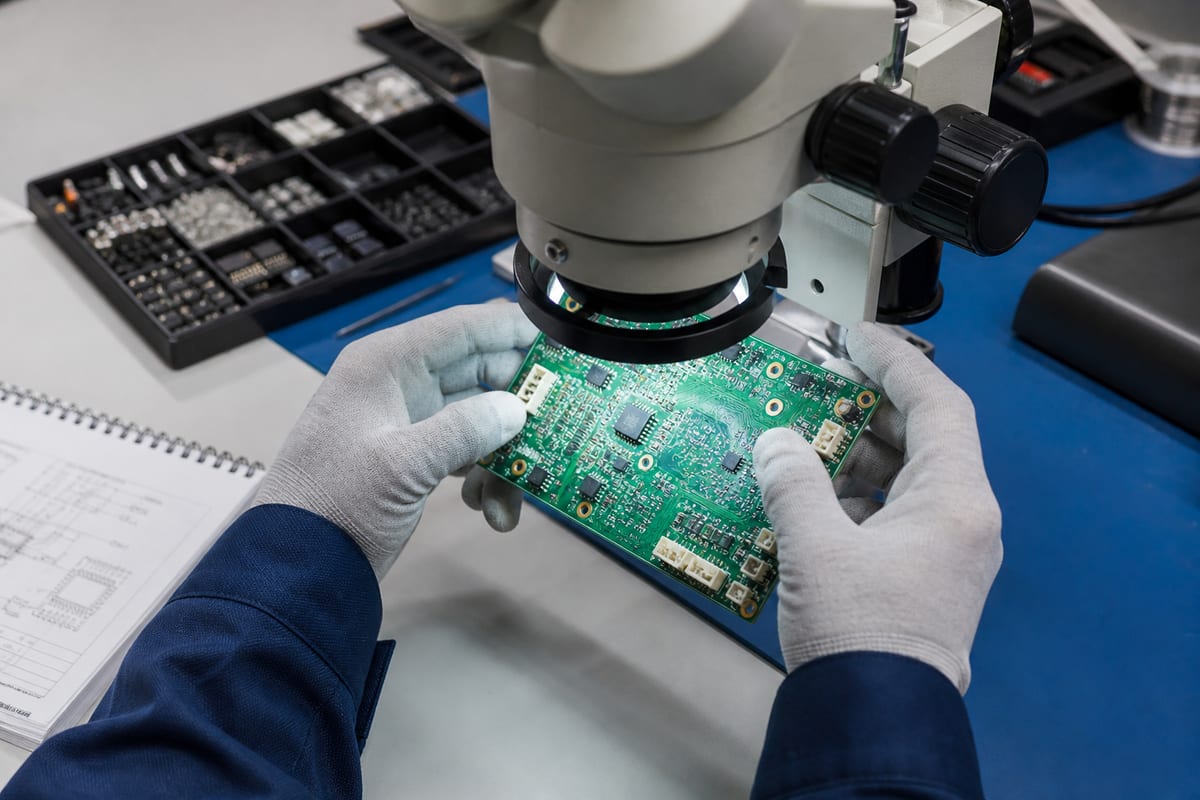
Small DFN and QFN packages need extra care because most solder joints are hidden under the component. AOI can confirm placement and visible features, but X-ray inspection may be needed to assess hidden joints or an exposed thermal pad. The inspection requirement should be agreed before assembly rather than added after a problem appears.
Digipot BOM, Sourcing, and Substitution Checks
The BOM should list the complete manufacturer part number, not only the resistance and package. It is also helpful to include the interface, number of channels, tap count, memory type, and temperature grade so that purchasing can distinguish between similar versions.
A proposed alternate should be checked for more than pin compatibility. Two parts can fit the same pads but use different commands, start at different wiper positions, or have different limits for terminal voltage and wiper current.
Check an alternate in four areas:
- Package: pinout, dimensions, height, and land pattern.
- Electrical performance: resistance, tolerance, wiper resistance, voltage, current, bandwidth, and temperature range.
- Digital operation: interface timing, address or command format, reset behavior, and memory operation.
- Supply status: source, traceability, lifecycle, moisture condition, lead time, and available quantity.
If the alternate requires a firmware change, the updated firmware version should be released with the BOM change. The contract manufacturer can provide sourcing information, but the design owner should approve the replacement before it is used.
Electronic Potentiometer PCBA Inspection and Testing
Assembly inspection and functional testing serve different purposes. AOI can detect many placement, polarity, marking, and visible solder defects. X-ray can provide information about joints hidden under the package. Neither test confirms that the digipot produces the correct analog output when it receives a command.
| Possible problem | Useful production evidence | Information needed from the customer |
|---|---|---|
| Wrong part or suffix | Package marking and BOM check | Approved MPN and alternates |
| Wrong orientation or soldering | First-article inspection, AOI, and X-ray where needed | Assembly drawing and acceptance requirements |
| Wrong startup setting | Power-cycle test and initial output measurement | Required startup value and timing |
| Incorrect adjustment | Minimum, midpoint, and maximum command tests | Commands, test points, and output limits |
| Setting is not retained | Write, power-off, restart, and readback test | Required memory behavior |
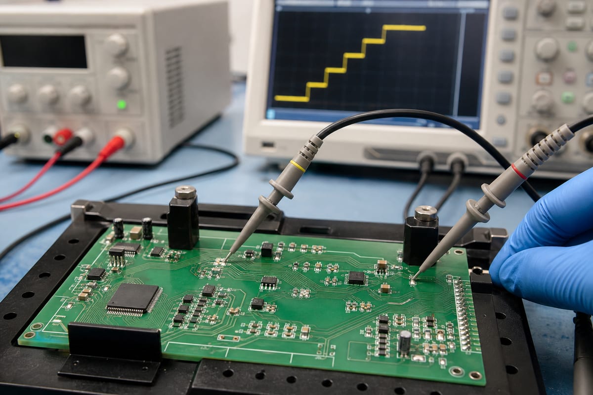
A practical test instruction identifies the power supply, connection points, commands, expected outputs, tolerances, and records to keep. Testing three or more wiper positions is usually more informative than checking communication alone. The limits should come from the complete circuit because wiper resistance, loading, temperature, and surrounding components all affect the measured result.
A Digital Potentiometer PCBA Project Example
One customer’s project used a four-layer FR-4 PCB with a finished thickness of 1.6 mm, TG170 material, and 2 oz finished copper on the outer and inner layers. The board had an ENIG finish, blue solder mask, white silkscreen, and a minimum hole-copper requirement of 25 µm.
The customer reviewed the production data before fabrication. The bare PCBs received electrical testing, and the assembly requirements included SMT, AOI, X-ray, test images, board cleaning, individual-board delivery, and antistatic packaging.
The project record does not specify whether a digital potentiometer was fitted. For a digipot on this type of PCBA, the manufacturing package would also need:
- The BOM and assembly drawing should show the complete part number, package, and Pin 1 orientation.
- The inspection plan should state whether the package has hidden joints that require X-ray.
- The functional test should send defined commands and measure the output at minimum, midpoint, and maximum settings.
- If the setting must survive a power cycle, the test should verify that behavior as well.
These checks confirm three different things: the bare PCB has no opens or shorts, the component is assembled correctly, and the completed circuit responds correctly to the control commands. All three results matter when a digital potentiometer is part of the design.
FAQs About Digital Potentiometer PCB Integration
Can a digital potentiometer directly replace any analog potentiometer?
No. Compare terminal voltage, wiper current, resistance, power, bandwidth, adjustment law, startup state, control method, and package. A circuit that works with a mechanical potentiometer may exceed the limits of a digipot.
Should I choose SPI or I2C for a digital potentiometer?
Choose the interface that fits the controller, available pins, bus architecture, speed, addressing, and firmware. Then check logic levels, pull-ups or chip select, reset behavior, and what happens when one device is unpowered.
Why does the measured output differ from the ideal tap value?
End-to-end tolerance, wiper resistance, loading, temperature, and surrounding components all affect the result. Use a worst-case circuit calculation to set limits, then confirm them on representative assemblies.
What should a digital potentiometer PCBA RFQ include?
Provide the approved PCB fabrication data, BOM with full MPNs, pick-and-place data, assembly drawings, approved alternates, test points, firmware or command requirements, and measurable acceptance limits.
What can EBest Circuit verify?
EBest Circuit (Best Technology) can support component sourcing, DFM review, PCB fabrication, PCBA, inspection, and testing to the requirements supplied with the order. Circuit design, component approval, firmware, and product-specific acceptance limits should be provided or approved by the customer. Send your files to sales@bestpcbs.com for review.