PCB manufacturing PCB manufacturing
Home > Blog

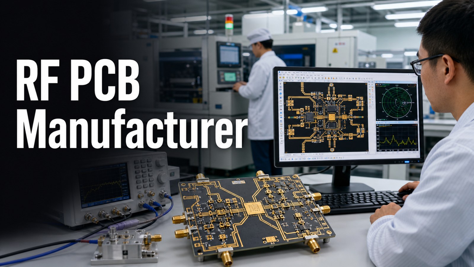
RF PCB Manufacturer

RF PCB Manufacturer for Controlled Signal Performance
Friday, July 17th, 2026
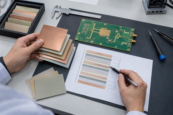
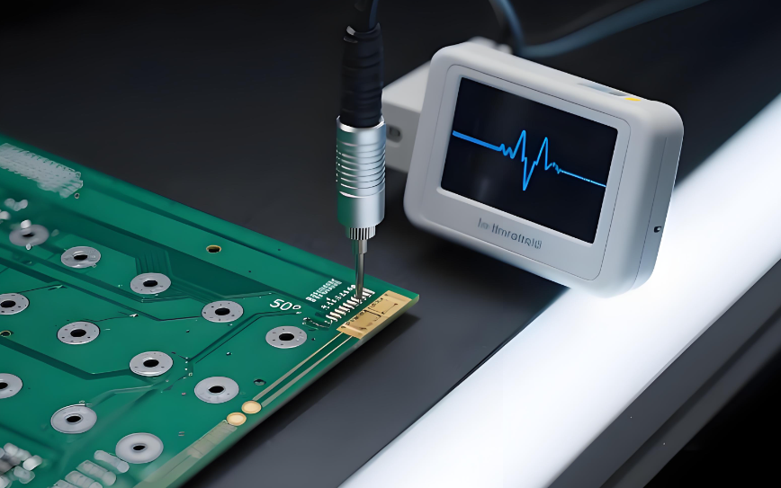
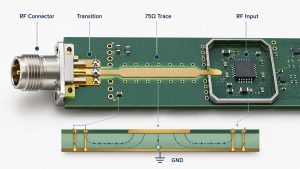
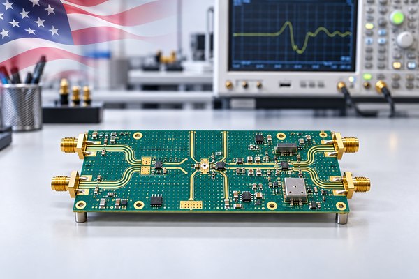
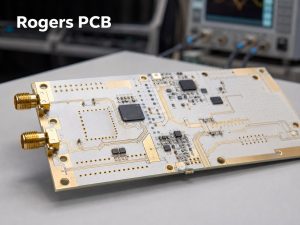
RF PCB manufacturer reviewing impedance traces and RF board testing

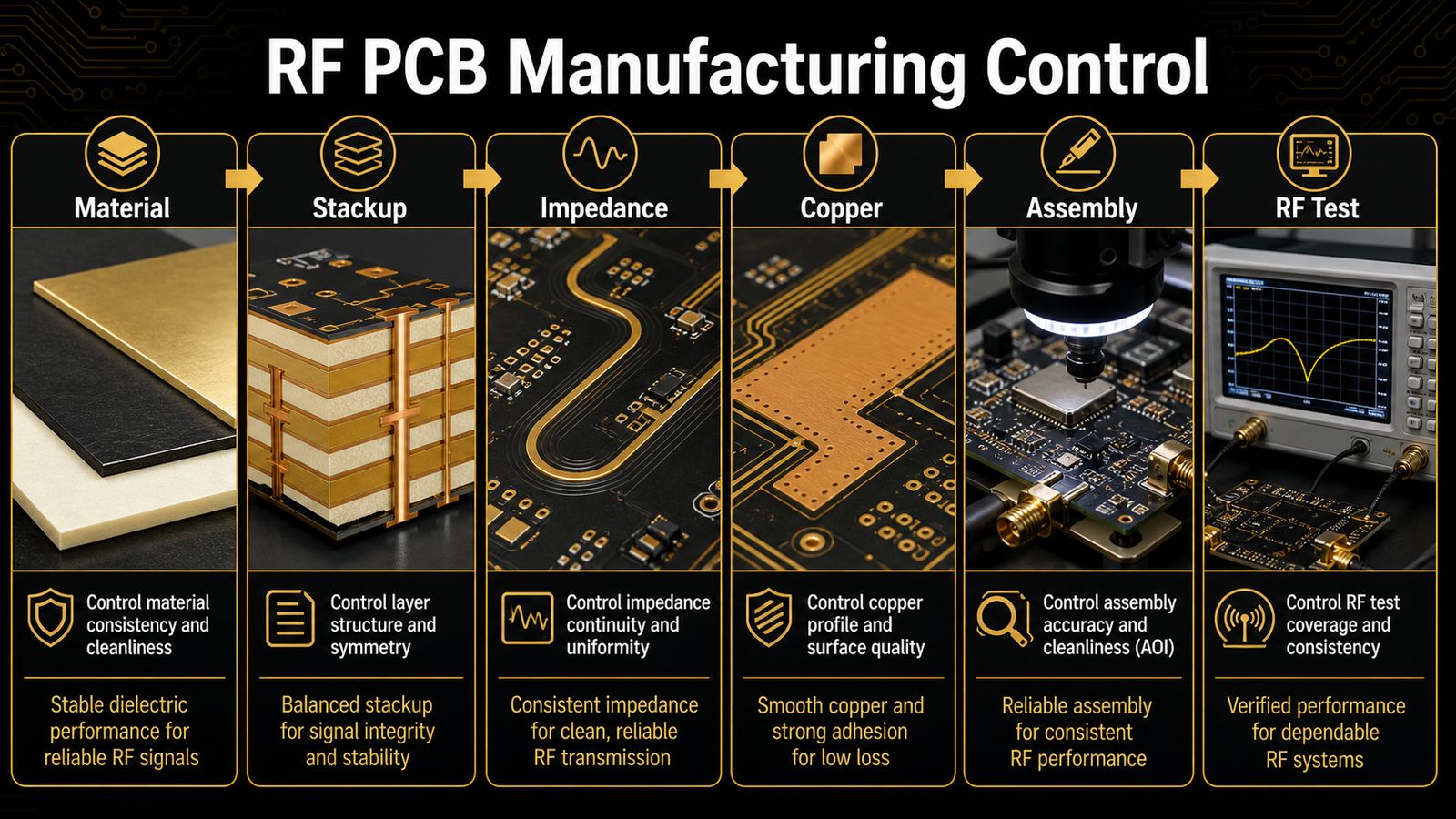
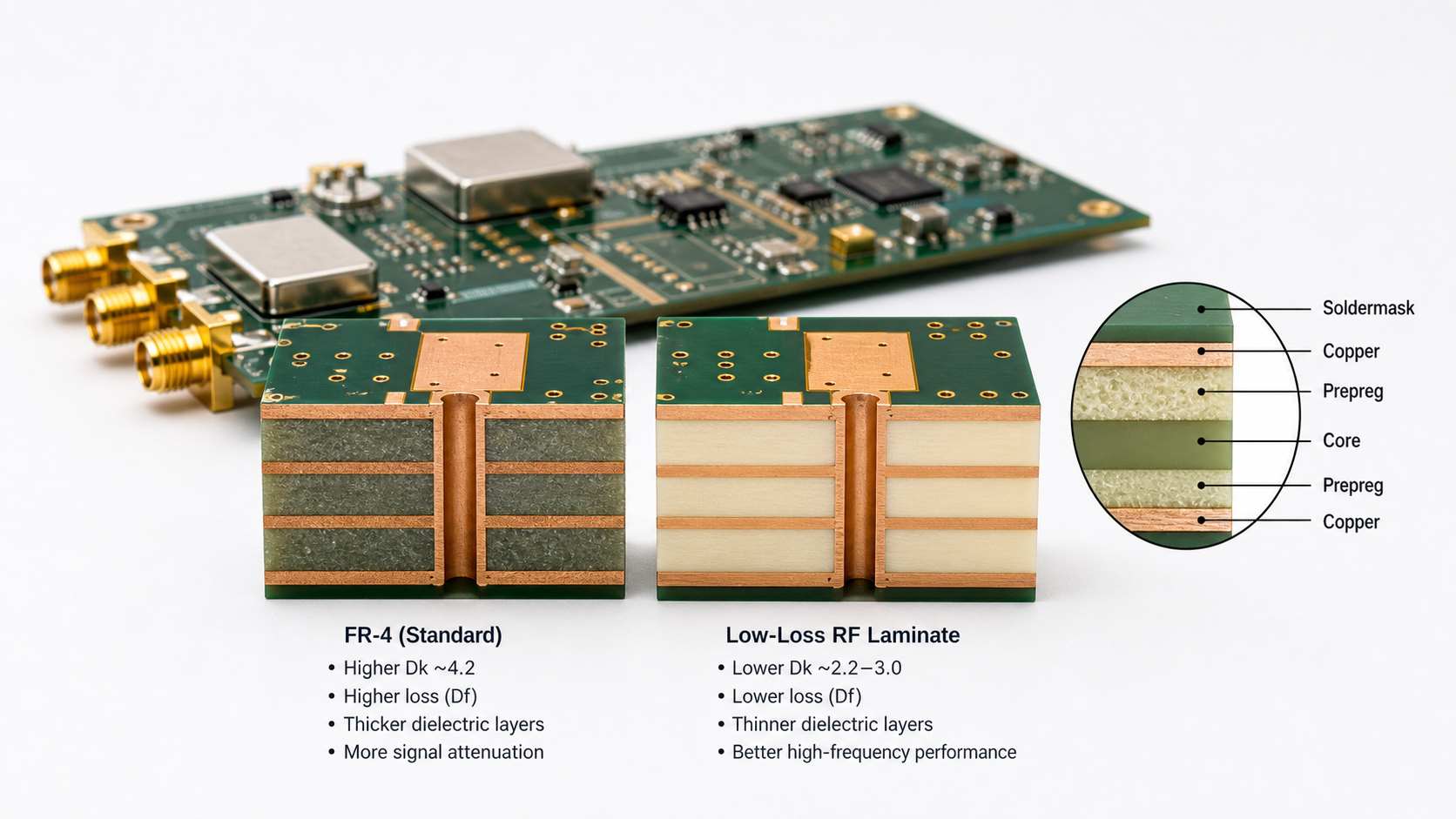
An RF PCB manufacturer must control material behavior, stackup, impedance, copper quality, fabrication accuracy, assembly details and test expectations, because small process changes can affect signal loss, reflection and final RF performance.

For buyers, choosing an RF PCB supplier is different from buying a simple FR-4 board. The quote should confirm whether the board needs Rogers, Taconic, PTFE, high-Tg FR-4, controlled impedance, special copper, RF connectors, PCBA, inspection or RF-related test documentation. EBest Circuit helps buyers review these requirements before the order moves into production.

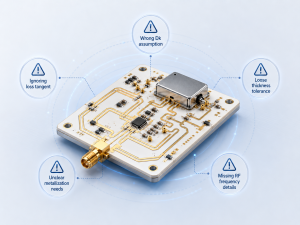
Is your RF PCB quote missing the details that decide signal performance?

RF PCB projects often become expensive when the supplier quotes the board like a normal rigid PCB.

  • The material name is selected, but laminate availability, stackup and processing route are not confirmed before quotation.
  • Impedance traces are drawn, but dielectric thickness, copper profile and reference planes are not reviewed together.
  • The design includes RF connectors or shielded sections, but assembly drawings, connector orientation and inspection access are checked too late.
  • The buyer needs repeatable RF performance, but the quote does not define what inspection, electrical test or RF-related documentation is expected.
  • The first supplier price looks lower, but later material substitution, stackup changes or DFM revisions reset the schedule.
EBest Circuit supports RF PCB buyers with engineering review before production:

  • We review Gerber or ODB++ files, stackup notes, impedance requirements, material preferences and RF connector details before quote assumptions are locked.

  • We can discuss high-frequency material options such as Rogers, Taconic, PTFE and high-Tg FR-4 based on the real project requirements and availability.
  • We connect RF PCB fabrication with PCBA, component sourcing, assembly drawings and inspection planning when the project needs assembled boards.
  • We flag DFM issues early, including trace geometry, copper balance, via structures, solder mask clearance, connector footprint and panelization.
  • We help buyers compare suppliers by build risk, communication quality, material route and quote clarity, not only by the first unit price.

What an RF PCB Manufacturer Must Control

An RF PCB manufacturer must control the full signal path, from laminate selection and stackup to copper quality, fabrication accuracy, assembly and testing.

RF boards are sensitive to dielectric behavior, copper surface, trace geometry, via transitions, ground design and connector placement. A supplier that only checks board outline and hole count may miss the factors that decide final performance. The best RF PCB quote should show that the manufacturer understands the board’s electrical function, not only its mechanical drawing.

Where RF PCB Projects Usually Lose Performance

RF PCB projects usually lose performance when design assumptions and manufacturing assumptions are not reviewed together.

Risk Area What Goes Wrong What to Confirm Before Quote
Material The selected laminate is not available or not suitable for the build route Material grade, thickness, availability and substitute rules
Stackup Reference planes, dielectric spacing and copper are not aligned with impedance needs Stackup drawing and controlled impedance notes
Fabrication Etching, copper, via and surface finish choices affect signal consistency Trace geometry, drill table, plating and finish requirements
Assembly Connector orientation, shield area or component placement creates rework BOM, CPL, assembly drawing and RF connector details
Testing The buyer expects RF performance evidence, but the quote only includes standard checks Inspection scope, electrical test and any RF-specific documentation needs

How EBest Circuit Helps RF PCB Buyers Reduce Build Risk

EBest Circuit helps RF PCB buyers reduce build risk by reviewing material, stackup, fabrication, PCBA and testing requirements before production starts.

For RF and microwave projects, we do not treat the board as a generic PCB. We ask for the files and constraints that influence performance: material preference, impedance notes, copper requirements, surface finish, RF connector details, assembly scope, test expectations and target delivery plan.

RF PCB Materials and Laminate Selection

RF PCB material selection should match signal performance, fabrication feasibility, assembly needs and sourcing availability.

EBest Circuit’s capability sources include high-frequency material references such as Rogers 4003, Rogers 4350, Rogers 5880, Taconic laminates, PTFE, Isola 370HR, FR408HR and high-Tg FR-4 options. The right choice depends on the project. Some materials require special confirmation, custom sourcing or project-specific lead-time review, so the material line should be confirmed before the buyer treats a quote as final.

Stackup, Impedance and Transmission Line Review

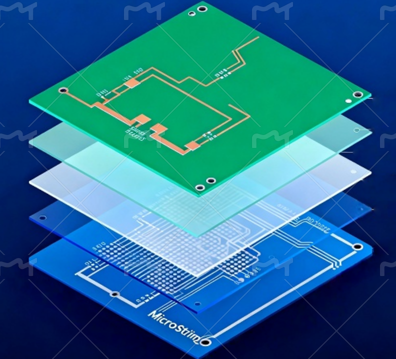
Stackup and impedance review should confirm how RF traces, dielectric layers, reference planes and copper work together.

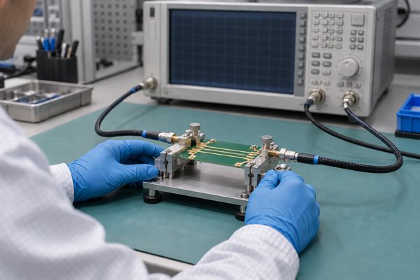
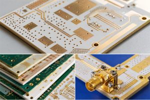
RF PCB manufacturing control from material to RF test

RF traces may use microstrip, stripline, coplanar or other controlled structures depending on the design. The manufacturer should understand which traces are critical, what impedance notes apply, and how the stackup will be built. If these details are missing, ask for DFM review before the order is released.

Copper, Etching, Surface Quality and Plating Control

Copper and etching quality affect RF transmission because trace profile, surface quality and plating choices can change signal behavior.

Buyers should provide critical trace details and avoid assuming that every copper or finish choice behaves the same. Surface finish should be selected based on assembly, contact needs, storage and RF performance expectations. If the design has tight RF lines, special materials or fine features, the fabrication route should be reviewed before price approval.

RF PCB Fabrication and Assembly Planning

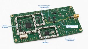
RF PCB fabrication should be planned with assembly when the board includes RF connectors, shielding, sensitive components or test fixtures.

Assembly details can affect RF performance after the bare board is finished. Connector alignment, solder joint quality, shielding, grounding, component placement and inspection access all matter. EBest Circuit can connect RF PCB fabrication with prototype PCB assembly, component sourcing and test planning when a project needs assembled boards.

RF Testing, Inspection and Documentation

RF PCB testing and inspection should be defined by the buyer’s product risk, not assumed from a generic PCB checklist.

Standard checks may include visual inspection, AOI, dimensional review and electrical test. RF-related validation may require additional project-specific instructions, fixtures or documentation. If your project needs special RF test evidence, include that requirement in the RFQ rather than adding it after production starts.

Cost and Lead-Time Factors for RF PCB Manufacturing

RF PCB cost and lead time depend on material selection, stackup complexity, impedance control, fabrication risk, assembly scope and test expectations.

Factor Why It Changes the Quote How Buyers Can Help
Material RF laminates and special substrates can change sourcing and lead time Provide approved material choices and substitute rules
Stackup Controlled dielectric and copper planning affect build route Send stackup and impedance notes early
Fabrication complexity Fine RF geometry, vias and finish requirements add review work Mark critical RF traces and tolerances clearly
Assembly RF connectors, shields and sensitive parts require careful handling Send BOM, CPL and assembly drawings with the PCB files
Testing Special validation can require fixtures, setup time or documentation Define test scope before quote approval

RF PCB Supplier Evaluation Checklist

An RF PCB supplier should be evaluated by material understanding, engineering response, fabrication control, assembly support and quote clarity.

  • Can the supplier discuss the material route and availability before final quote approval?
  • Does the supplier review stackup and impedance notes instead of quoting from outline and layer count only?
  • Can fabrication and PCBA be reviewed together when the product needs assembled boards?
  • Does the quote explain what inspection, electrical test and RF-related documentation are included?
  • Does the engineering team respond with practical DFM questions before production?

RFQ Checklist for RF PCB Manufacturing

A strong RF PCB RFQ should include design files, RF constraints, material preferences, assembly files and test expectations.

  • Gerber or ODB++ files, drill files and fabrication drawing
  • Stackup, material preference, dielectric notes and controlled impedance requirements
  • Critical RF trace notes, via structures, copper requirements and surface finish
  • BOM, CPL, assembly drawing, RF connector details and approved alternates if PCBA is needed
  • Inspection, electrical test, RF-related validation or documentation requirements
  • Quantity, prototype stage, forecast, packaging and target delivery plan

FAQ About Choosing an RF PCB Manufacturer

What is an RF PCB manufacturer?

An RF PCB manufacturer builds printed circuit boards for radio-frequency and microwave circuits where material behavior, impedance, copper quality, stackup and test planning can affect signal performance.

What should buyers send for an RF PCB quote?

Send Gerber or ODB++ files, drill files, stackup notes, material preference, controlled impedance requirements, BOM, CPL, assembly drawings, RF connector details, test expectations, quantity and target delivery plan.

Can EBest Circuit support Rogers or other RF materials?

EBest Circuit’s capability sources include RF material references such as Rogers, Taconic, PTFE and high-Tg FR-4 options. Final material availability and processing route should be confirmed against the specific project files and order requirements.

Should RF PCB fabrication and assembly be quoted together?

Yes, when the RF board includes connectors, shields, sensitive components or test requirements. Quoting PCB and PCBA together helps catch footprint, clearance, soldering and inspection issues earlier.

Need an RF PCB manufacturer for a prototype or production build? Send your Gerber or ODB++ files, stackup, material preference, impedance notes, BOM, CPL, RF connector details, test requirements, quantity and target delivery plan to sales@bestpcbs.com. EBest Circuit can review RF PCB fabrication, PCBA and quote risks before production starts.

You may also like

Radio Frequency Circuit Board: Materials, Design Rules, and Cost Factors
Thursday, July 9th, 2026

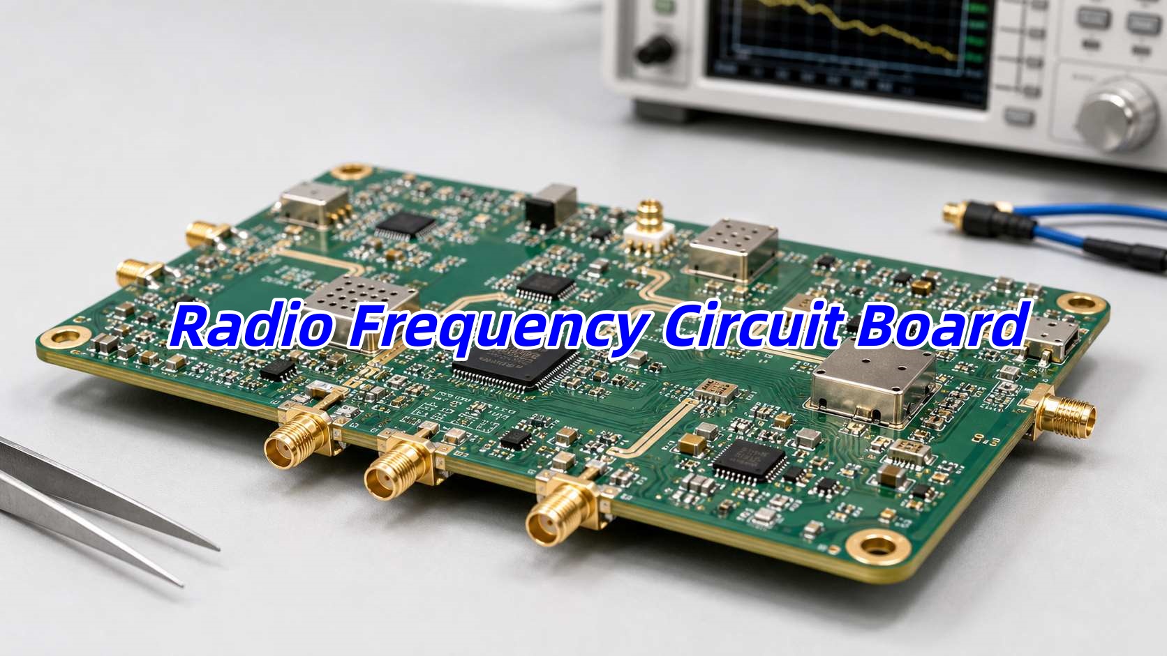
A radio frequency circuit board is a PCB designed to carry signals that are sensitive to impedance, loss, coupling, and electromagnetic behavior. In practical terms, that usually means the board layout, material choice, stackup, grounding, and connector transitions matter far more than they do on an ordinary low-speed control board.

Not every board that includes a wireless module called RF PCB. The term usually applies when the board itself must support controlled high-frequency signal behavior, such as RF transmission lines, matching networks, filters, antennas, mixers, LNAs, PAs, or microwave interconnects. Once the frequency rises, the board is no longer just a mechanical carrier. It becomes part of the circuit.

Radio Frequency Circuit Board

What Is a Radio Frequency Circuit Board?

A radio frequency circuit board, often called an RF PCB or high-frequency PCB, is a printed circuit board built for circuits that operate in the radio or microwave range. These boards are commonly used in wireless communication, radar, GPS, satellite systems, RF test equipment, automotive telematics, industrial sensing, medical devices, and IoT products.

The key difference from a standard FR-4 board is not just frequency. It is electrical predictability. An RF design needs controlled impedance, stable dielectric behavior, low insertion loss, good return paths, and a layout that limits radiation and coupling.

That is why the same schematic can behave very differently depending on the PCB material, copper geometry, via structure, and connector launch design.

When Is a Standard PCB Not Enough for RF Applications?

Many projects start on standard FR-4 because it is familiar and cost-effective. In some RF products, that is still the right choice. But once signal integrity, loss, or repeatability become tight, ordinary stackups may not be enough.

In general, a standard PCB becomes less suitable when the project includes:

  • Controlled RF transmission lines
  • High-frequency amplifiers or filters
  • Antennas integrated on the board
  • Low-loss signal paths over meaningful distance
  • Tight phase or impedance consistency
  • Microwave connectors and launch structures
  • Multi-band or high-gain RF front ends

If a design only carries short RF traces between a certified module and an antenna connector, FR-4 may still be acceptable. If the board itself contains tuned RF structures, matching sections, or long controlled signal paths, material selection becomes much more critical.

When Is a Standard PCB Not Enough for RF Applications?

Common Materials Used for RF Circuit Boards

The material decision is usually driven by dielectric constant stability, dissipation factor, temperature behavior, moisture absorption, and manufacturability.

Material TypeTypical UseMain AdvantageMain Trade-Off
Standard FR-4Lower-cost RF modules, mixed digital/RF boards, short RF tracesLow cost and easy fabricationHigher loss and less stable dielectric behavior
High-speed FR-4 / low-loss epoxyMid-range RF and mixed-signal boardsBetter loss performance than standard FR-4Still not ideal for demanding microwave designs
PTFE-based laminatesMicrowave, radar, satellite, low-loss RF pathsVery low loss and stable RF behaviorHigher material cost and more demanding processing
Hydrocarbon ceramic laminatesRF and microwave products needing a balance of cost and performanceBetter dimensional and RF stabilityMore expensive than ordinary FR-4
Hybrid stackupsMixed RF and digital boardsLets engineers control cost by using RF material only where neededLamination and DFM complexity increase

For many buyers, the important point is this: the best RF material is not always the most expensive one. It is the one that meets loss, impedance, and stability targets without adding unnecessary fabrication difficulty.

How Material Properties Affect RF PCB Performance?

At RF frequencies, the substrate is an electrical design variable, not just a base material.

The most important properties are:

  • Dielectric constant (Dk): affects trace width, signal velocity, and impedance control
  • Dissipation factor (Df): affects dielectric loss and insertion loss
  • Thickness tolerance: affects impedance repeatability
  • Copper surface profile: affects conductor loss at higher frequencies
  • Thermal stability: matters for power amplifiers and outdoor products
  • Moisture absorption: matters for frequency stability and reliability in harsh environments

If the dielectric constant shifts too much across frequency or production lots, the board can move off target even when the fabrication dimensions look correct.

RF PCB Stackup and Impedance Control

A radio frequency circuit board should be designed with the stackup settled early, not after routing is nearly done.

That is because the stackup controls:

  • Microstrip or stripline impedance
  • Reference plane continuity
  • Return current path quality
  • Trace spacing and coupling
  • Connector launch geometry
  • Via transition behavior

Most RF boards rely on microstrip or grounded coplanar waveguide structures on outer layers, because they are easier to tune and measure. Stripline can work well too, especially where shielding and coupling control matter more than easy tuning access.

Key Layout Rules for a Radio Frequency Circuit Board

At RF, a board can fail even when the schematic is correct. Layout decisions directly affect gain, noise, return loss, spurious response, and EMC behavior.

The most important layout rules usually include:

  • Keep RF traces short and direct
  • Avoid unnecessary layer transitions
  • Maintain continuous reference planes
  • Control trace width and spacing from the beginning
  • Isolate noisy digital, clock, and power-switching areas from sensitive RF paths
  • Place matching components close to the device pins they tune
  • Keep the ground via fence strategy consistent around critical RF regions
  • Minimize stubs at connectors, pads, and test access points

For higher-frequency boards, even pad shape, solder mask opening, and connector footprint transitions can noticeably change performance.

Why Grounding Matters More in RF PCB Design?

Grounding problems are one of the most common reasons RF boards behave differently in prototype, validation, and mass production.

A good RF ground system is not just “more copper.” It requires a predictable return path. Gaps in reference planes, poor stitching around transmission lines, and mixed return currents from digital and RF sections can all degrade performance.

In practical RF layouts, engineers often use:

  • Solid reference planes under RF traces
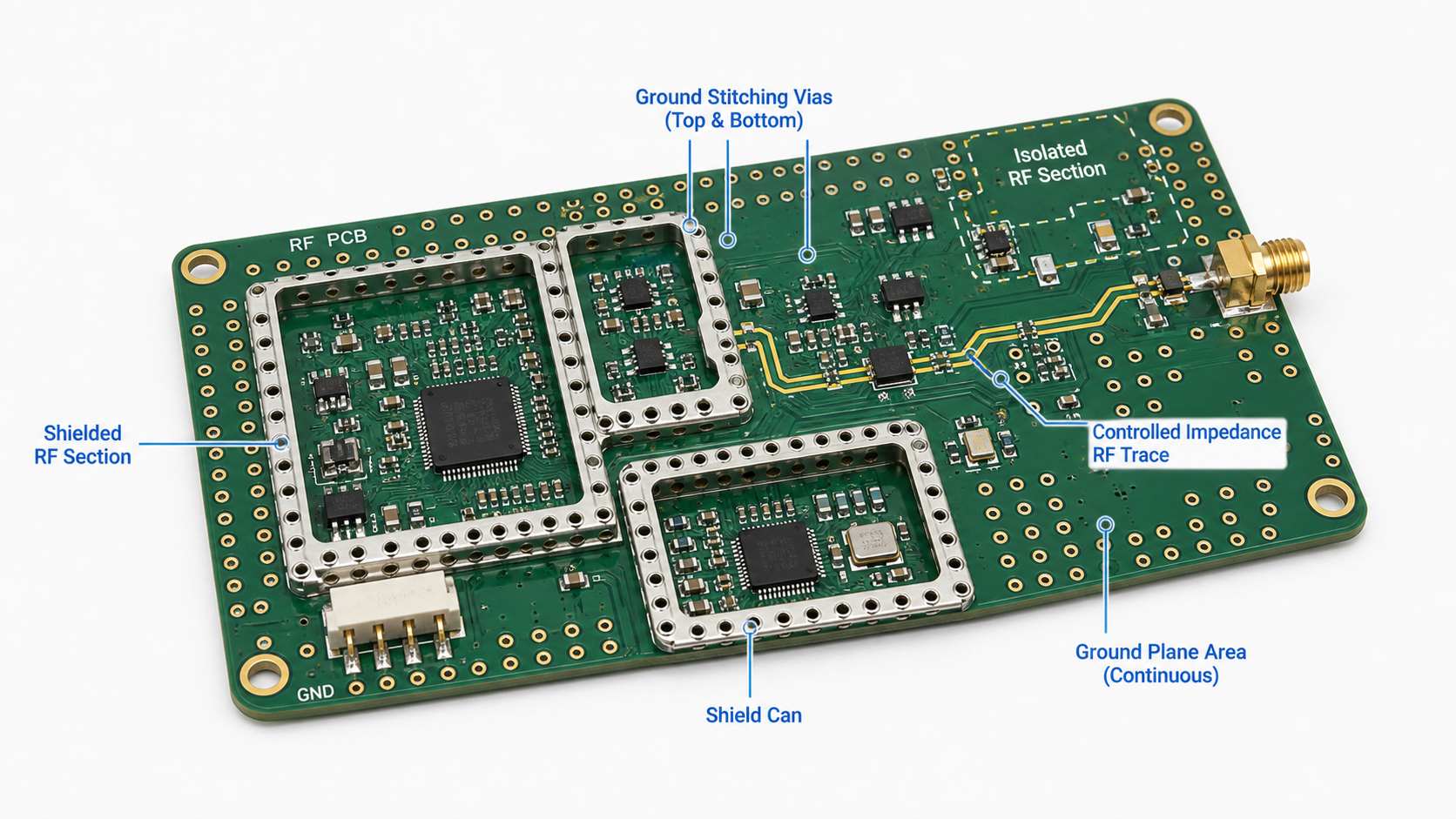
  • Stitching vias around RF boundaries and connector launches
  • Controlled grounding around antennas and shield cans
  • Partitioning between RF, analog, digital, and power sections

If the grounding strategy is weak, the board may show unstable tuning, increased loss, or unexpected radiation.

Why Grounding Matters More in RF PCB Design?

Vias, Connectors, and Transitions in High-Frequency Boards

At lower frequencies, vias and connectors are mostly interconnect details. At RF, they are part of the transmission path.

The decision logic is simple: every transition adds discontinuity, so transitions should be limited and designed intentionally.

RF Transition ElementMain ConcernPractical Design Focus
Signal viaInductance and impedance discontinuityReduce unnecessary transitions and optimize return path vias
Connector launchReflection and mismatchTune pad shape, anti-pad, and ground stitch pattern
Test point or stubAdded discontinuity and radiationAvoid on critical RF traces when possible
SMA or edge connector areaMechanical fit and RF continuityKeep launch geometry consistent with stackup
Board-to-board RF pathCoupling and lossShort path, controlled impedance, stable connector system

If the project includes microwave connectors, the launch region should usually be reviewed as a separate RF structure, not treated as a standard footprint.

Can FR-4 Be Used for a Radio Frequency Circuit Board?

Yes, but only within the right application boundary.

FR-4 can still be acceptable when:

  • RF frequency is modest
  • RF path is short
  • Insertion loss is not extremely tight
  • The design uses a certified RF module and the host board only carries short matched traces
  • Cost sensitivity is higher than peak RF performance

FR-4 becomes less attractive when:

  • Design includes long RF paths
  • Can be operates at higher microwave frequencies
  • phase consistency matters
  • Includes integrated antennas or distributed RF structures
  • Needs low loss and repeatable tuning across production lots

In other words, FR-4 is not “wrong.” It is just not universal.

Typical Applications of RF Circuit Boards

A radio frequency circuit board can appear in many industries, but the design priorities are not always the same.

Common applications include:

  • Wireless communication equipment
  • GPS and GNSS devices
  • Wi-Fi, Bluetooth, and IoT hardware
  • RF power amplifiers and front-end modules
  • Radar and sensing systems
  • Medical telemetry devices
  • Automotive RF electronics
  • Satellite and aerospace communication hardware
  • RF test and measurement equipment

For example, an IoT gateway may care most about mixed-signal integration and manufacturability, while a radar board may care more about loss, phase stability, and controlled transitions.

Manufacturing Challenges of RF PCBs

RF boards are often harder to manufacture consistently than standard digital boards because electrical behavior is tied closely to fabrication details.

The most common manufacturing challenges include:

  • Tighter impedance tolerance requirements
  • Laminate handling differences for PTFE-based materials
  • Dimensional stability during lamination
  • Copper roughness effects at higher frequency
  • Drill quality and registration around controlled transitions
  • Hybrid stackup bonding complexity
  • Solder mask influence near RF launch areas

That is why DFM review matters early. A board that works in simulation but ignores real fabrication tolerances can become expensive to debug later.

This is also where EBest Circuit (Best Technology) can be useful. For RF-related PCB or PCBA projects, the practical value is not just fabrication capacity. It is the ability to review stackup, manufacturability, material choice, and assembly fit before the project enters production.

RF PCB Assembly and Testing Considerations

RF assembly is not just ordinary SMT with different parts. Placement accuracy, connector alignment, shielding, cleaning control, and test setup can all affect final performance.

Important assembly and test concerns include:

  • Connector coplanarity and solder quality
  • Shield can placement and rework access
  • Stability of matching network components
  • Board cleanliness, especially where leakage or detuning matters
  • Cable and fixture repeatability during validation
  • Test method selection such as VNA measurement, insertion loss, return loss, or gain verification

For RF PCBA projects, buyers should also think ahead about whether they need bare-board delivery, assembly only, tuned prototype support, or functional RF test support.

What to Provide When Requesting a Quote for an RF Circuit Board

A useful RF quotation needs more than “board size and layer count.”

The most helpful files and notes usually include:

  • Gerber or ODB++ files
  • Layer stackup
  • Target impedance and trace type
  • Material preference or acceptable alternatives
  • Operating frequency range
  • Copper thickness
  • Connector type and launch details
  • Assembly requirement if PCBA is needed
  • RF test requirement if applicable
  • Prototype quantity and production forecast

If the board includes a special RF laminate, hybrid stackup, controlled launch area, or microwave connector, that should be stated clearly in the inquiry. Otherwise, the supplier may quote the board as if it were a standard PCB, which creates avoidable back-and-forth later.

How to Choose the Right RF PCB Manufacturer?

The right RF PCB supplier is not simply the one with the lowest laminate price. The better question is whether the supplier can support the actual engineering risk of the design.

A good evaluation checklist includes:

  • Experience with RF and high-frequency materials
  • Ability to support hybrid stackups if needed
  • Impedance control capability
  • Understanding of connector launch and grounding details
  • Assembly support for RF components and shielding
  • Test and inspection capability aligned with the product
  • Willingness to review DFM issues before build

For engineers moving from prototype into production, EBest Circuit’s one-stop PCB manufacturing, component sourcing, PCBA assembly, and technical review model can reduce handoff mistakes, especially when the design mixes RF, digital control, and power sections on one board.

Conclusion

A radio frequency circuit board is not just a normal PCB running at a higher speed. It is a board whose electrical behavior depends strongly on material properties, stackup structure, grounding, trace geometry, and transitions. The right material and layout choices depend on the actual RF function, not just the frequency number alone.

If you are evaluating an RF PCB or RF PCBA project, the most practical approach is to define the frequency range, loss target, impedance structure, material options, and assembly requirements early. For RF PCB and PCBA support, contact EBest Circuit at sales@bestpcbs.com.

You may also like

RF Board
Friday, April 10th, 2026

What Is an RF PCB?

RF board, or Radio Frequency Printed Circuit Board, is engineered for circuits operating at high frequencies where signal integrity becomes highly sensitive to material properties. Typical RF designs work in the range of 300 MHz to 3 GHz, and many advanced systems extend far beyond this.

At these frequencies, standard FR4 materials often fail to maintain stable dielectric performance and low signal loss. As a result, specialized high frequency laminates are required. RF PCBs are therefore built using materials with low dielectric loss (Df) and stable dielectric constant (Dk) to ensure consistent signal transmission.

RF board is ideal for applications with higher operating frequency requirements. Right now, we normally use following material:

These boards are widely used in applications such as:

  • Wireless communication systems
  • RF antennas and modules
  • Automotive radar (ADAS)
  • Satellite and aerospace electronics
  • Microwave devices
  • IoT and high-speed signal systems

Why Use RF PCB Instead of Standard FR4?

FR4 is cost-effective and widely used, but its dielectric properties vary significantly at high frequencies. This leads to signal loss, impedance instability, and reduced system reliability in RF designs.

RF PCB materials solve these issues by offering:

  • Lower signal loss at high frequency
  • More stable dielectric constant across frequency range
  • Better impedance control
  • Reduced signal distortion
  • Improved phase consistency

What Materials Are Used in RF PCB?

Material selection is the core of RF PCB performance. Different applications require different dielectric properties and processing characteristics.

Common RF PCB Materials

1. Rogers Laminates

Widely used in RF and microwave circuits due to balanced performance and manufacturability.

Typical grades include:

  • RO4003C
  • RO4350B
  • RO4233

These materials offer:

  • Stable dielectric constant
  • Low loss tangent
  • Good thermal reliability

2. PTFE-Based Materials (Teflon)

Used in more demanding RF designs where ultra-low loss is critical.

Advantages:

  • Extremely low dielectric loss
  • Excellent high frequency performance

Considerations:

  • More complex processing
  • Higher manufacturing cost

Copper Thickness Range

  • Standard: 1/4 oz to 2 oz
  • Custom: based on current load and thermal design


Rogers is often the practical choice for most RF designs, while PTFE is used when performance requirements are more demanding.

Rogers Laminate Material Parameters

Choosing the right Rogers material directly affects signal integrity, impedance stability, and insertion loss. Below is a comparison of commonly used Rogers laminates for RF PCB applications.

MaterialDielectric Constant (Dk @10GHz)Loss Tangent (Df @10GHz)Thermal Conductivity (W/m·K)Typical Application
RO4350B3.48 ±0.050.00370.62General RF, antennas, automotive radar
RO4003C3.55 ±0.050.00270.71RF communication, microwave circuits
RO42333.30 ±0.050.00250.65High frequency, low loss applications
RT58802.20 ±0.020.00090.20Ultra-low loss, aerospace, high-end RF
RO30033.00 ±0.040.00130.50High stability circuits, precision RF
RO301010.2 ±0.250.00230.95High dielectric designs, compact circuits

RF Board Capability

  • Base material: Rogers/Telfon
  • Board Thickness: 0.5mm~3.0mm(0.02″~0.12″)
  • Copper thickness: 0.5 OZ, 1.0 OZ, 2.0 OZ, 3.0 OZ
  • Outline: Routing, punching, V-Cut
  • Soldermask: White/Black/Blue/Green/Red Oil
  • Legend/Silkscreen Color: Black/White
  • Surface finishing: Immersion Gold, HASL, OSP
  • Max Panel size: 600*500mm(23.62″*19.68″)
  • Packing: Vacuum/Plastic bag
  • Samples L/T: 7~9 Days
  • MP L/T: 8~10 Days

RF PCB FAQs

1. What frequency requires RF PCB instead of FR4?

Typically, designs above 1 GHz or requiring strict impedance control should consider RF materials. Lower frequencies may still use FR4 depending on performance tolerance.

2. Is Rogers better than FR4?

For high frequency applications, yes. Rogers offers lower loss and more stable dielectric properties, which improves signal integrity.

3. Why is PTFE PCB more expensive?

PTFE materials are harder to process and require specialized manufacturing steps, which increases production cost.

4. Can RF PCB be used for mixed signal designs?

Yes. Hybrid stackups combining RF materials and FR4 are commonly used to balance performance and cost.

Start Your RF PCB Project Today

If you are designing RF or microwave circuits, choosing the right PCB is critical to performance.

At Best Technology, we combine material expertise, process control, and engineering support to deliver reliable RF PCB solutions.

📩 Send your design files to: sales@bestpcbs.com

Our engineering team will review your project and provide a fast quotation with optimization suggestions.

You may also like

Top 10 RF PCB Manufacturers in USA | Trusted RF PCB Manufacturer Guide
Friday, December 19th, 2025

Choosing the right RF PCB manufacturer in the USA directly affects signal integrity, insertion loss, and long-term product reliability. In RF systems operating above 1 GHz, even a ±5% variation in dielectric constant (Dk) or ±1 mil trace deviation can cause impedance mismatch and measurable signal degradation.

For applications such as 5G base stations, radar modules, satellite communication, medical imaging, and defense electronics, RF PCBs demand more than standard multilayer fabrication. This guide reviews the top 10 RF PCB manufacturers in the USA, explains how they were evaluated, and helps buyers identify what truly defines a capable RF PCB manufacturing partner.

Top 10 RF PCB Manufacturers in USA | Trusted RF PCB Manufacturer Guide  https://www.bestpcbs.com/blog/2025/12/top-10-rf-pcb-manufacturers-in-usa/

What Is an RF PCB Manufacturer?

An RF PCB manufacturer is a factory equipped to control high-frequency electrical behavior, not just fabricate boards using RF laminates.

A qualified RF PCB manufacturer typically demonstrates:

  • Controlled impedance tolerance of ±5–10%
  • Proven experience with Rogers, Taconic, PTFE, and hybrid RF stack-ups
  • Line width and spacing control down to ±1 mil
  • RF-aware stack-up and grounding validation
  • Process consistency between prototype and volume production

Unlike standard digital PCBs, RF designs are sensitive to copper roughness, resin distribution, and prepreg variation. Manufacturers without RF-specific process control often struggle to deliver repeatable RF performance.

Common Challenges When Choosing an RF PCB Manufacturer in the USA

Despite the strong PCB ecosystem in the USA, RF buyers frequently encounter the following issues:

  • Impedance drift between batches, especially in volume production
  • Limited experience with hybrid RF stack-ups (Rogers + FR-4)
  • RF performance verified only at prototype stage, not scaled production
  • Long RF laminate lead times (often 4–6 weeks)
  • Minimal engineering feedback beyond Gerber fabrication

According to industry feedback, over 30% of RF PCB project delays are caused by material handling or impedance inconsistencies rather than design errors. This highlights why RF capability must be validated beyond certifications.

Common Challenges When Choosing an RF PCB Manufacturer in the USA https://www.bestpcbs.com/blog/2025/12/top-10-rf-pcb-manufacturers-in-usa/

How We Evaluated the Top RF PCB Manufacturers in the USA?

Manufacturers were evaluated using practical RF manufacturing benchmarks, not marketing claims.

Key evaluation criteria included:

  • RF material portfolio (Rogers RO4350B, RO4003C, RO5880, Taconic, PTFE)
  • Demonstrated impedance control capability (≀ ±10%)
  • Experience with multilayer RF and mixed-signal designs
  • Quality certifications relevant to RF applications
  • Ability to support prototype + mid-volume production

Factories focusing only on RF prototyping without scalable production control were ranked lower.

Top 10 RF PCB Manufacturers in USA

RankCompany NameRF PCB CapabilityKey AdvantagesLocation
1TTM TechnologiesRF & microwave multilayersDefense & aerospace expertiseCalifornia
2SanminaHigh-reliability RF PCBsEnd-to-end manufacturingCalifornia
3Summit InterconnectRF multilayer & HDIQuick-turn RF capabilityCalifornia
4Advanced CircuitsRF prototypesFast turnaroundColorado
5Sierra CircuitsHigh-frequency fabricationStrong DFM supportCalifornia
6Rush PCBRF proto & low volumeCost efficiencyCalifornia
7Epec Engineered TechnologiesRF & mixed-signal PCBsIntegrated PCBAMassachusetts
8Green CircuitsRF PCB manufacturingEMS integrationCalifornia
9All Flex SolutionsRF flexible circuitsSpecialty RF flexMinnesota
10APCTComplex RF multilayersAdvanced stack-upsCalifornia

Are US RF PCB Manufacturers Always the Best Choice?

US RF PCB manufacturers offer clear advantages:

  • Local engineering communication
  • ITAR and defense compliance
  • Established aerospace and telecom experience

However, buyers should also consider:

  • Higher manufacturing costs (often 30–50% above offshore)
  • Limited RF laminate inventory
  • Less flexibility for mid-volume scaling

As a result, many OEMs now adopt a hybrid sourcing strategy, using US suppliers for early development and qualified offshore RF PCB manufacturers for volume production.

US RF PCB Manufacturers 
https://www.bestpcbs.com/blog/2025/12/top-10-rf-pcb-manufacturers-in-usa/

Global Alternative RF PCB Manufacturer for USA Customers

As RF projects become more globalized, many USA companies now evaluate global RF PCB manufacturers that offer comparable RF performance with better lead time, cost flexibility, and material availability. Below is a representative list of global RF PCB manufacturers serving high-frequency and microwave applications, based on manufacturing capability, RF material experience, and export readiness.

RankCompany NameCountry / RegionRF PCB CapabilityKey Strengths for USA Customers
1EBest Circuit (Best Technology)China / VietnamRF, microwave, hybrid stack-upsFast lead time, wide RF materials, 30–50% cost advantage
2AT&SAustriaRF, high-frequency, IC substratesHigh-end RF technology, EU quality standards
3UnimicronTaiwanRF, HDI, high-speedAdvanced multilayer RF capability
4CompeqTaiwanRF & high-speed PCBsStable mass production for RF designs
5Meiko ElectronicsJapanRF & automotive PCBsHigh reliability, automotive RF experience
6Shennan CircuitsChinaRF & telecom PCBsStrong telecom and RF infrastructure
7IbidenJapanRF & package substratesPrecision RF manufacturing
8KinwongChinaRF & mixed-signal PCBsCost-effective RF volume production
9Chin Poon IndustrialThailandRF & automotive PCBsSoutheast Asia manufacturing flexibility
10Dynamic ElectronicsTaiwanRF multilayer PCBsMature RF fabrication processes

Why Global Buyers Choose EBest Circuit (Best Technology) as an Experienced RF PCB Manufacturer?

EBest Circuit (Best Technology) supports RF PCB programs with a focus on repeatability and manufacturability, not just RF materials.

Our RF PCB capability includes:

  • Rogers, Taconic, Isola, and hybrid RF stack-ups
  • Controlled impedance down to ±8%
  • RF trace width control to ±1 mil
  • Multilayer RF boards up to 20+ layers
  • ISO 9001, ISO 13485, IATF 16949, and AS9100D certified systems
  • MES-based traceability for materials and process control

This enables USA customers to transition smoothly from prototype to volume production without RF performance drift.

FAQs

1. What materials do RF PCB manufacturers typically use?

Common materials include Rogers RO4000/RO5000 series, Taconic, PTFE, and selected low-loss FR-4.

2. Is FR-4 suitable for RF PCB applications?

FR-4 is generally suitable below 1 GHz; higher frequencies benefit from low-loss laminates.

3. How do RF PCB manufacturers control impedance?

Through stack-up modeling, dielectric thickness control, copper roughness management, and process calibration.

4. What is the typical lead time for RF PCB prototypes?

Most RF PCB prototypes ship within 7–12 working days, depending on material availability.

5. How can I verify an RF PCB manufacturer’s RF capability?

Review impedance data, RF material history, similar project experience, and quality certifications.

You may also like

RF PCB Manufacturer: Complete Guide to Materials and Design Considerations
Thursday, December 18th, 2025

An RF PCB manufacturer specializes in the design and fabrication of printed circuit boards used in radio-frequency, microwave, and high-frequency electronic systems. As operating frequencies increase, PCB performance is no longer determined only by connectivity, but by electromagnetic behavior, material stability, and manufacturing precision.

This pillar page provides a comprehensive, engineering-focused overview of RF PCB manufacturing. It covers what an RF PCB manufacturer does, how RF PCBs differ from standard boards, RF frequency definitions, materials, stackup design, manufacturing processes, common mistakes, and how to evaluate RF PCB manufacturing capability.

What Is an RF PCB Manufacturer?

An RF PCB manufacturer is a PCB supplier with specialized expertise in producing circuit boards for applications operating at radio frequencies, typically above 30 MHz. At these frequencies, PCB traces act as transmission lines, and small variations in geometry or material properties can significantly affect signal integrity.

Compared with standard PCB manufacturers, RF PCB manufacturers must control:

  • Dielectric constant (Dk) stability across frequency and temperature
  • Dissipation factor (Df) to minimize insertion loss
  • Tight impedance tolerance, often ±5% or better
  • Copper surface roughness, which directly affects high-frequency loss
  • Stackup symmetry and lamination consistency

These requirements mean RF PCB manufacturing is as much an electromagnetic discipline as a mechanical one.

What Is an RF PCB Manufacturer?   https://www.bestpcbs.com/blog/2025/12/rf-pcb-manufacturer/

What Is an RF PCB Manufacturer?

RF PCB vs Standard PCB (Quick Comparison)

Although RF PCBs and standard PCBs may look similar in appearance, they are fundamentally different in design philosophy, material selection, and manufacturing control. As frequency increases, even small variations that are acceptable in standard PCBs can cause severe performance degradation in RF designs.

Key Differences Between RF PCB and Standard PCB

Comparison ItemRF PCBStandard PCB
Typical operating frequency>30 MHz up to GHz/mmWaveDC to low-speed digital
Signal behaviorTransmission-line dominatedLumped-circuit dominated
Primary design concernImpedance, loss, phase stabilityConnectivity and routing
Core materialsRogers, PTFE, Taconic, RF laminatesFR-4
Dielectric constant (Dk)Tightly controlled, frequency-stableWider tolerance
Dissipation factor (Df)Low-loss requiredLess critical
Copper surface roughnessStrictly controlledUsually not critical
Impedance tolerance±5% or tighter±10% common
Stackup complexityHigh, often hybridRelatively simple
Manufacturing difficultyHighModerate
Cost sensitivityPerformance-drivenCost-driven

In short, standard PCB manufacturing prioritizes manufacturability and cost, while RF PCB manufacturing prioritizes electrical performance and consistency. This is why RF PCBs must be produced by a qualified RF PCB manufacturer rather than a general PCB supplier.

What Frequency Range Is Considered RF in PCB Manufacturing?

In PCB manufacturing, RF generally refers to frequencies above 30 MHz, where wavelength becomes comparable to trace dimensions and transmission-line effects dominate.

Typical frequency classifications include:

  • 30 MHz – 300 MHz: VHF
  • 300 MHz – 3 GHz: UHF and microwave
  • 3 GHz – 30 GHz: Microwave and millimeter-wave

As frequency increases, the impact of dielectric variation, copper roughness, and impedance mismatch becomes more severe, requiring stricter manufacturing controls.

RF PCB Frequency Range https://www.bestpcbs.com/blog/2025/12/rf-pcb-manufacturer/

Common RF PCB Materials

Material selection is one of the most important responsibilities of an RF PCB manufacturer. RF materials are chosen for predictable dielectric behavior and low signal loss across frequency.

Typical RF PCB Materials

  • Rogers RO4003C / RO4350B – Widely used RF laminates with stable Dk
  • Rogers RO3003 / RO3006 – Microwave and millimeter-wave applications
  • Taconic RF materials – Cost-effective RF solutions
  • PTFE-based laminates – Ultra-low loss for high-frequency designs

A qualified RF PCB manufacturer evaluates materials based on frequency range, insertion loss targets, thermal performance, and manufacturability.

RF PCB Applications

RF PCBs are used in applications where signal integrity at high frequency is critical.

Common RF PCB applications include:

  • 5G and cellular base stations
  • RF front-end modules and power amplifiers
  • Automotive radar systems (24 GHz, 77 GHz)
  • Satellite and aerospace communication systems
  • Wireless IoT, Wi-Fi, and Bluetooth modules

Each application places different requirements on materials, stackup, and manufacturing precision.

RF PCB Manufacturing Process (Simplified)

RF PCB manufacturing requires tighter process control than standard PCB fabrication.

A simplified RF PCB manufacturing flow includes:

RF PCB Manufacturing Process  https://www.bestpcbs.com/blog/2025/12/rf-pcb-manufacturer/

1. RF laminate handling and moisture control

2. Precision drilling to prevent dielectric deformation

3. Copper etching with controlled surface roughness

4. Sequential lamination for hybrid RF/FR-4 stackups

5. Impedance-controlled trace patterning

6. Electrical testing and impedance verification

Consistency across batches is critical, as even small process variations can affect RF performance.

RF PCB Stackup Design Considerations

Stackup design directly influences impedance stability, loss, and manufacturability.

Key stackup considerations RF PCB manufacturers must control include:

  • Uniform dielectric thickness
  • Stable Dk across all RF layers
  • Continuous and uninterrupted reference planes
  • Compatibility between RF laminates and FR-4 prepregs
  • Controlled lamination sequence to avoid warpage

In many cases, RF PCB manufacturers collaborate with customers to finalize stackups before production.

Common RF PCB Manufacturing Mistakes

RF PCBs are highly sensitive to manufacturing errors.

Common RF PCB manufacturing mistakes include:

  • Using inappropriate materials for the target frequency
  • Ignoring copper roughness effects on insertion loss
  • Poor stackup symmetry causing mechanical distortion
  • Etching variation leading to impedance mismatch
  • Lack of RF-specific design-for-manufacturing review

Experienced RF PCB manufacturers reduce these risks through upfront engineering validation and strict process control.

Why Choose EBest Circuit (Best Technology) as Your RF PCB Manufacturer?

When evaluating RF PCB manufacturing capability, EBest Circuit (Best Technology) is often selected due to its strong focus on RF and high-frequency PCB production. With experience in RF materials, controlled impedance manufacturing, and RF-focused engineering support, EBest Circuit (Best Technology) demonstrates the core capabilities expected from a professional RF PCB manufacturer.

By choosing EBest Circuit (Best Technology), customers benefit from:

  • Proven RF and microwave PCB manufacturing experience
  • Tight impedance and material control
  • Engineering-driven process validation
  • Reliable performance for high-frequency applications

For projects involving RF, microwave, or high-speed communication systems, selecting EBest Circuit (Best Technology) as your RF PCB manufacturer helps reduce technical risk and improve overall product reliability.

FAQs About RF PCB Manufacturing

1. What does an RF PCB manufacturer do?

    An RF PCB manufacturer produces printed circuit boards optimized for high-frequency performance, focusing on impedance control, low signal loss, and material stability.

    2. Can FR-4 be used in RF PCB manufacturing?

    FR-4 may be acceptable for low-frequency RF designs, but at higher frequencies it suffers from higher loss and unstable dielectric properties.

    3. Why are RF PCBs more difficult to manufacture?

    RF PCBs are sensitive to small variations in materials, geometry, and processing, making manufacturing control critical.

    4. Are RF PCBs more expensive than standard PCBs?

    RF PCBs typically cost more due to specialized materials, tighter tolerances, and additional process controls.

    You may also like

    Are RF PCB and High-Frequency PCB the Same?
    Tuesday, December 9th, 2025

    Not exactly. All RF PCBs fall under the high-frequency PCB category, but not all high-frequency PCBs qualify as RF PCBs.

    RF PCB work sits at the center of many wireless systems, and an RF PCB often looks similar to a high frequency pcb. Many designers ask if they are the same board. They are related, yet each one handles different needs in signal flow, layout control, and material behavior.

    As we move deeper into 5G, radar modules, and clean wireless designs, the differences become more visible. This article explains those differences in simple, clear language. More importantly, it guides engineers, buyers, and project teams on how to choose the right board for their next product.

    What Is an RF PCB?

    An RF PCB full name is Radio Frequency PCB, which is specifically handles signals in the radio frequency range: typically 300 MHz to 300 GHz, including microwave and millimeter-wave designs.

    RF PCBs involve much stricter engineering constraints:

    • Tight impedance (<±5%) on microstrip, grounded CPW, stripline
    • Precise feature control (trace width tolerance around ±0.01–0.03 mm)
    • Stable dielectric properties across temperature
    • Very low-loss materials such as RO3003, RO4350B, RO5880, Taconic RF-35, PTFE woven/non-woven
    • Specialized stackups to avoid parasitic radiation
    • Careful via design to avoid stubs and resonance

    Applications include:

    • Radar systems
    • Satellite communication
    • LNBs
    • RF front-end modules
    • Power amplifiers
    • Filters, couplers, antennas

    RF PCB is wider use of 5G, IoT, and compact antennas has created strong demand for high-grade rf pcb builds. Because the signals travel along microstrip or CPW structures, the board behaves like part of the RF device, not only a carrier.

    What Is a High-Frequency PCB?

    A high-frequency PCB is any printed circuit board operating above roughly 500 MHz to 10 GHz+, depending on the design community.

    These boards focus on:

    • Stable dielectric constant (Dk tolerance ±0.02–0.05)
    • Low dissipation factor (Df) for reduced signal loss
    • Good impedance control across long traces
    • Suitable materials like Rogers RO4003C, RO4350B, RO3003, PTFE, Isola I-Tera MT40, etc.

    High-frequency PCBs serve applications such as:

    • 5G modules
    • Wi-Fi devices
    • GPS receivers
    • High-speed digital layouts (DDR4/DDR5, SerDes)

    High frequency boards focus on clean rise times, controlled impedance, and manageable dielectric loss. They support Wi-Fi, Bluetooth, high-speed digital lines, and mixed-signal designs. The design margin is wider than rf pcb work because the board deals with digital pulses, not pure RF energy.

    high frequency pcb

    High Frequency PCB

    Key Differences Between RF PCB vs. High Frequency PCB

    AspectHigh-Frequency PCBRF PCB
    DefinitionBoards operating at high digital or analog frequenciesBoards designed specifically for RF signal transmission
    Signal Range500 MHz–10 GHz+300 MHz–300 GHz
    Design FocusSignal integrity, low lossElectromagnetic control, transmission lines, matching
    MaterialRogers 4000 series, Isola, Panasonic MegtronPTFE, RO3003/5880, ceramic-filled laminates
    Impedance ControlImportantCritical (tighter tolerance)
    Manufacturing DifficultyMediumHigh
    Typical UseWi-Fi, Bluetooth, high-speed digitalRadar, RF amplifiers, filters, GNSS, mmWave

    When Are They “the Same PCB”?

    A design can fall under both categories when:

    • The signal is RF (e.g., 2.4 GHz, 5.8 GHz)
    • The designer uses high-frequency materials
    • The board contains microstrip, CPW, filters, or antennas

    For example, a 2.4 GHz RF transceiver board using RO4350B is simultaneously:

    • a high-frequency PCB, because frequency is high
    • an RF PCB, because it processes RF signals

    Thus, overlap exists, but they are not inherently identical.

    Which One Should You Specify to Your PCB Supplier?

    If your project handles RF transmission, always specify RF PCB so the manufacturer focuses on:

    • surface roughness control (Ra < 2 ”m for low loss)
    • uniform dielectric thickness
    • controlled resin flow during lamination
    • tighter etching tolerance
    • Dk matching for microstrip/CPW accuracy

    If it is only high-speed digital (e.g., PCIe, SerDes), then choose high-frequency PCB.

    Why Do RF PCBs Need Special Materials Compared with High Frequency PCBs?

    Material behavior influences both categories. Yet an rf pcb is more sensitive to the dielectric constant and copper profile.

    RF units run energy through transmission lines. If the copper roughness increases loss, the system sees reduced range or gain shift. If the Dk drifts, the phase response moves. Because of this, the most common materials for rf pcb work include RO3003, RO4350B, RO5880, and PTFE blends.

    In contrast, high frequency pcb materials can include Megtron series or Rogers 4000 series because the signal shape is less sensitive to phase stability. They still target low loss, but their working window is wider.

    Why Do RF PCBs Need Special Materials Compared with High Frequency PCBs?

    What Frequencies Define RF PCB Work vs High Frequency PCB Work?

    Both ranges relate to how the signal behaves. RF work usually starts at 300 MHz and goes up to millimeter-wave. This includes radar, satellite, GPS, 24 GHz and 77 GHz systems, and many short-range radios.

    High frequency ranges start from about 500 MHz to beyond 10 GHz. These support fast digital buses, Wi-Fi, and mixed-signal designs.

    However, the frequency alone does not decide the board’s category. The final system function does.

    Do RF PCBs Always Cost More Than High Frequency PCBs?

    Actually yes when under the same design. RF boards use premium materials. These materials cost more because they hold stable Dk, low loss, and a smooth copper surface. They also require strict process control during drilling, plating, and lamination.

    High frequency boards may use moderate-cost materials such as RO4003C or Megtron 4. They also need controlled lamination, yet the window for yield is wider.

    Costs also rise when an rf pcb uses fine lines, tight impedance, or stacked microstrip structures. That said, skilled manufacturers can keep RF costs under control by optimizing stackup and process flow.

    What Problems Occur When Designers Use the Wrong PCB Type?

    If a design intended for RF is built on a standard high frequency pcb, several issues may appear:

    • Reduced communication range
    • Higher insertion loss
    • Unstable gain
    • Incorrect antenna tuning
    • Phase delay changes
    • EMC issues

    Although not every situation is severe, these issues waste time in testing and rework.

    When a high frequency digital board is produced using strict RF rules, the design remains stable. Yet the cost often rises without a visible performance gain.

    What Tests Are Important for RF PCBs Compared with High Frequency PCBs?

    RF boards often need tests beyond regular PCB checks. These include:

    • Dielectric thickness check
    • Dk variation review
    • Copper profile check
    • TDR impedance scan
    • S-parameter review after assembly

    High frequency boards may also use TDR scans, yet the tolerance is wider. For RF, every shift affects the final device.

    How Does EBest Circuit (Best Technology) Support RF PCB and High Frequency PCB Projects?

    EBest Circuit (Best Technology) offers full material guidance, stackup review, transmission line advice, and strong quality assurance for both rf pcb and high frequency pcb builds. We handle small prototype lots and volume orders with the same care. Each rf pcb passes a detailed review, so the final product meets the performance target.

    Our strengths include:

    • ISO9001, ISO13485, IATF16949, and AS9100D systems
    • Complete MES traceability
    • Tight impedance control
    • Fine etching for RF lines
    • Skilled process teams for PTFE and hybrid stackups
    • Smooth copper profile management
    • Fast prototype to mass build for global clients

    We support antenna work, radar modules, filters, amplifiers, and mixed-signal boards. Our engineering team reviews each design before production to catch layout risks early to speed up product launches. For your next RF or high frequency project, our team stands ready to guide you from concept to delivery!

    FAQs

    1. Is an rf pcb the same as a high frequency pcb?

    No. All RF boards are high frequency boards, but not all high frequency boards meet RF conditions.

    2. Can I use RO4003C for both RF and high frequency PCB use?

    Yes. However, many RF systems still need lower-loss materials such as RO3003 or RO5880.

    3. Are RF boards harder to build?

    Yes. They need tighter process control, smoother copper, and stable lamination.

    4. How do I know if my design needs an rf pcb?

    If your design uses antennas, filters, couplers, or PA modules, you need an RF board.

    5. Does EBest Circuit (Best Technology) support RF and high frequency PCBA work?

    Yes. We handle full assembly, tuning, connector installation, and testing.

    You may also like

    What is Radio Frequency PCB? RF PCB Design Guidelines
    Tuesday, December 2nd, 2025

    When it comes to wireless systems—WiFi, Bluetooth, cellular IoT, radar, GPS, or any RF module—the performance of the radio frequency PCB (RF PCB) directly determines signal integrity, radiation efficiency, and product stability. A radio frequency PCB operates in high-frequency environments where small layout changes may shift impedance, weaken gain, or create unwanted noise. Because of this, a radio frequency PCB requires strict engineering rules, carefully selected materials, and a routing method that protects signal quality.

    This article explains what an RF PCB is, the characteristics you must consider, the right FR PCB materials, the correct RF PCB routing rules, and a complete RF PCB design guideline you can follow for your next high-frequency design. Hope this guide is helpful and give you a best solution to design your RF PCB.

    What is Radio Frequency PCB? RF PCB Design Guidelines

    What Is a Radio Frequency PCB?

    A radio frequency PCB, or RF PCB, refers to a board used to transmit and receive signals at high frequencies—from hundreds of megahertz to multiple gigahertz. These boards are widely used in wireless modules, IoT devices, GPS systems, consumer electronics, radar sensors, and communication infrastructure.

    Unlike standard FR4 boards, RF PCBs involve dedicated dielectric materials, controlled impedance structures, and strict layout rules to keep signal integrity stable. The entire PCB—from stack-up to routing—must support predictable propagation velocity, stable loss characteristics, and smooth energy flow.

    RF PCBs are used in:

    • Wireless modules
    • GPS receivers
    • Sub-GHz transmitters
    • 5G communication units
    • Radar sensors
    • IoT devices
    • RF amplifiers and mixers
    • Antenna feed circuits

    Their performance depends on trace geometry, ground stability, and how cleanly the RF path is designed.

    What Is a Radio Frequency PCB?

    What Is a Radio Frequency PCB?

    Characteristics of an RF PCB

    RF PCBs typically have the following characteristics:

    • Controlled impedance routing for RF signal paths
    • Low-loss PCB materials to minimize attenuation
    • Stable dielectric constant (Dk) over temperature and frequency
    • Strict EMI/EMC requirements
    • Short, direct RF trace routing
    • Careful grounding strategy (dedicated ground plane, stitching vias)
    • Special treatment around matching networks and antenna feeds

    Because RF energy behaves like waves rather than simple electrical current, the PCB becomes part of the RF system itself—meaning the layout, stack-up, and materials must be engineered for high-frequency behavior.

    What Is the Frequency Range of RF PCB?

    RF PCBs typically operate in the following ranges:

    Frequency BandRangeTypical Applications
    Low RF300 MHz – 1 GHzISM band, sub-GHz transmitters
    Mid RF1 GHz – 6 GHzWi-Fi, Bluetooth, GPS
    High RF6 GHz – 30 GHz5G, radar
    Millimeter Wave30 GHz – 80 GHzAutomotive radar, high-speed links

    Most IoT devices today (BLE, WiFi, Zigbee, Sub-GHz RF) fall between 433 MHz – 6 GHz.

    What Is the Best PCB Material for RF?

    Choosing the right laminate affects signal quality, trace accuracy, and overall loss.

    • FR4 PCB Material

    FR PCB material, typically FR4, works for low-frequency RF designs below 2.4 GHz. It offers low cost and good mechanical strength. However, its dielectric properties vary with temperature and frequency. Loss tangent is higher than PTFE, so it works best for short RF paths or low-power consumer wireless modules.

    • Rogers RF Materials

    Rogers laminates such as RO4350B, RO4003C, and RO5880 are widely used for RF designs due to:

    • Low loss tangent
    • Very stable dielectric constant
    • Smooth copper surface
    • High processing consistency

    These materials are ideal for GPS, radar, Wi-Fi 6, UWB, sub-6G, and millimeter-wave applications.

    • PTFE / Teflon Laminates

    PTFE offers excellent RF performance, especially for microwave and radar. It has very low loss and highly stable characteristics. Fabrication needs tight process control due to soft substrate behavior.

    • Ceramic Substrates

    Ceramics substrate provide strong thermal stability and high dielectric precision. They work well in high-power RF amplifiers, satellite communication modules, and advanced radar systems.

    Here is a common radio frequency PCB material table:

    SubstrateTg (°C)Td (°C)DkLoss TangentBand
    FR4~135~295< 4.4~0.022 (parasitic ignored)X–K
    Isola MT402003603.38–3.750.0028–0.0035W
    IS680 AG-3482003603.480.0029W
    IS680 AG2003603.00–3.480.0020–0.0029W
    IS6802003602.80–3.450.0025–0.0035W
    Isola MT772003603.000.0017W
    Rogers 3003NR5003.000.0013W
    Rogers 3006NR5006.150.0022X–Ka
    Rogers 4360>2804076.150.0038X–Ka
    RT Duroid 6010.2LMNR50010.700.0023X–Ka
    RT Duroid 6202NR5002.900.0015X–Ka
    RT Duroid 6006NR5006.450.0027X–Ka
    RT Duroid 6035NRNR3.500.0013X–Ka

    (Note: NR means Not Reported)

    PCB Design Guide for Radio Frequency RF Boards

    Designing RF PCBs involves stack-up planning, controlled impedance, grounding, spacing, matching networks, and EMI reduction. Below are the recommended RF PCB guidelines and routing rules you can apply to achieve stable wireless performance.

    1. Start With Complete RF Design Information

    Successful RF PCB design begins long before the first trace is drawn. Engineers must collect all essential RF parameters to avoid redesigns later. This includes:

    • Functional description and operating frequency band
    • Current and voltage requirements of each RF stage
    • RF component list and package dimensions
    • PA gain, receiver sensitivity, and system isolation targets
    • Planned PCB stack-up structure
    • Controlled impedance values
    • Mechanical constraints and enclosure limits
    • Shielding frame or metal-can dimensions
    • Matching network reference designs
    • Simulation results for power amplifiers and LNAs

    Gathering this information early ensures that layout decisions align with system-level RF performance.

    PCB Design Guide for Radio Frequency RF Boards

    PCB Design Guide for Radio Frequency RF Boards

    2. Physical Zoning of the RF PCB

    Physical zoning organizes the board according to how RF signals flow.

    • RF Signal Flow Placement

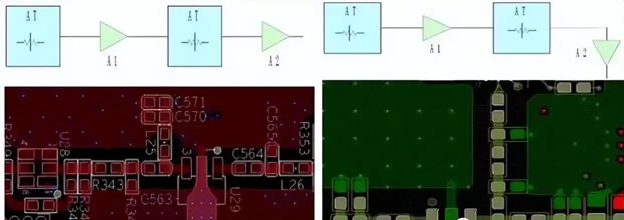
    Place RF components in the exact order of the signal chain. A short, direct, and linear path minimizes insertion loss, improves impedance stability, and preserves gain.

    • RF Component Orientation

    Rotate filters, PAs, LNAs, couplers, and mixers so their input/output pins align with the straightest possible RF path. Avoid unnecessary detours or bends.

    • Isolation Through Ground Structures

    To prevent RF coupling and cross-interference, isolate RF sections using:

    • Ground shielding walls
    • Via-fence structures
    • Shield cans over sensitive circuits
    • Copper barriers or partitions

    These structures keep RF and digital noise apart, improving overall stability.

    PCB Design Guide for Radio Frequency RF Boards

    3. Electrical Zoning

    Electrical zoning separates different circuit domains so they cannot interfere with each other.

    • Power section: Power management ICs, regulators
    • Digital control section: MCUs, logic circuits, clocks
    • Analog RF section: LNAs, PAs, filters, mixers, antennas

    These zones should not overlap in routing. Digital switching noise or PLL jitter can easily couple into RF paths if the layout is not properly divided.

    4. RF Transmission Line Structures

    RF PCBs commonly use one of three controlled-impedance transmission line types:

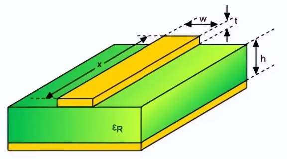
    Microstrip Line

    • RF trace on the top layer
    • Continuous ground plane directly beneath (Layer 2)
    • Impedance determined by trace width and dielectric height
    • Ideal for simple and low-to-mid–frequency RF designs.
    Microstrip Line

    Stripline

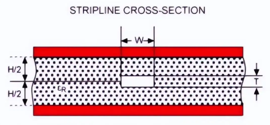
    • RF trace routed on an inner layer
    • Sandwiched between two solid ground planes
    • Provides superior isolation and uniform impedance
    • Useful in compact or high-frequency designs where shielding is critical.
    Stripline

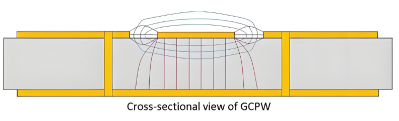
    Grounded Coplanar Waveguide (GCPW)

    • Top-layer trace with ground on both sides
    • Ground plane below the trace
    • Excellent isolation and impedance control
    • Often preferred when space is tight or when multiple RF lines run in parallel.
    Grounded Coplanar Waveguide (GCPW)

    5. Impedance Selection and Calculation

    Achieving the correct characteristic impedance (typically 50Ω) requires considering:

    • Trace width
    • Copper thickness
    • Dielectric constant (Dk)
    • Dielectric height between layers

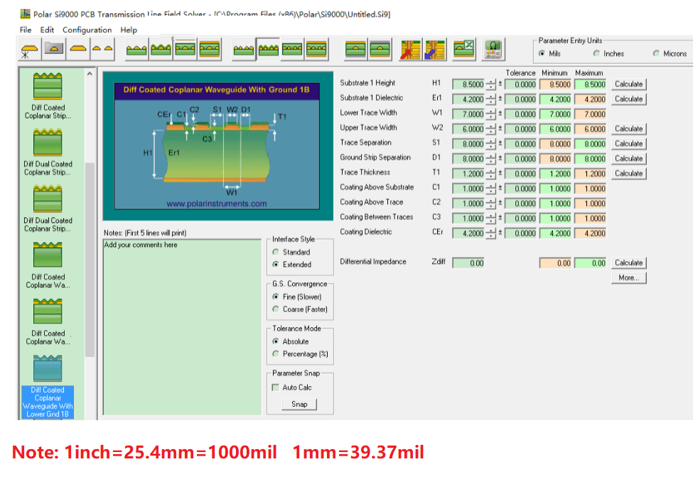
    Use tools such as Polar SI9000 or your PCB manufacturer’s impedance calculator.

    Impedance Selection and Calculation

    6. RF Trace Bending Rules

    Straight RF traces are ideal, but bends are sometimes unavoidable.

    Follow these rules:

    • Minimum bend radius ≄ 3× trace width
    • Avoid 90° bends (cause impedance discontinuity)
    • Use 45° bends or smooth arc/bowed shapes
    • Apply mitering to compensate for impedance changes

    For critical RF links, simulate bends in an EM solver to validate performance.

    7. Layer Transitions for RF Traces

    RF traces should stay on one layer. If a layer change is unavoidable:

    • Use two vias at minimum
    • Via diameter should match the RF trace width
    • When space is tight, use three smaller vias in parallel

    Multiple vias reduce via inductance and minimize impedance mismatch.

    8. Signal Isolation Rules

    Isolation is as important as impedance control in RF design.

    a) RF Lines

    • Keep RF traces well separated
    • Avoid long parallel runs
    • Use GCPW for noisy or densely packed areas
    • Keep sensitive microwave lines away from high-power circuits

    b) High-Speed Digital Signals

    • Route digital clocks on different layers
    • Avoid crossing beneath RF paths
    • Switching noise can modulate RF signals if not isolated

    c) Power Lines

    • Use a dedicated power layer for stable distribution
    • Place bypass capacitors close to RF IC power pins
    • Keep power traces away from RF transmission lines

    9. Ground Area Design

    Ground integrity determines the quality of RF performance.

    • Use solid, continuous ground planes
    • Avoid slots, gaps, and return-path interruptions
    • Do not route signals across RF ground regions
    • Add abundant ground stitching vias
    • Reduce inductance in ground loops

    In RF PCB design, a 4-layer RF PCB design is widely considered the most balanced structure for modern wireless modules because it provides stable impedance, strong isolation, and efficient routing without dramatically increasing manufacturing cost. While 2-layer boards are cheaper and 6-layer boards offer more routing space, the 4-layer stack-up delivers the best performance-to-cost ratio for most RF applications under 6 GHz.

    Below is the recommended stack up:

    • Layer 1 (Top Layer): RF traces + components
    • Layer 2 (Ground Plane): Continuous ground reference
    • Layer 3 (Power Plane): Power routing + local shielding below RF areas
    • Layer 4 (Bottom Layer): Non-critical routing or power distribution

    RF PCB Routing Rules You Must Follow

    1. The length of the RF traces should be kept as short as possible, and ensure that the surrounding densely arranged holes are shielded. The intervals should be approximately 50 mils.

    2. RF traces must not have vias, meaning they cannot cross layers. It is preferable to use 135° angle traces or circular traces.

    3. Near the RF traces, there should be no high-frequency signal lines. Pay attention to the UART signal line being shielded by a ground layer, and add ground holes around it for protection.

    4. The RF traces should be as close as possible to the size of the pads.

    5. For the RF traces, matching networks and the area around the antenna socket > 0.8mm, copper cannot be laid; they need to be hollowed out.

    6. The RF traces should be kept as far away from the battery holder as possible, with a distance of at least 5mm or more.

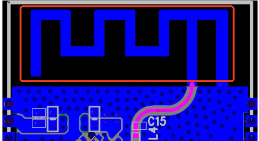
    7. A π-type matching circuit needs to be reserved on the RF path, and this π-type matching circuit should be placed close to the chip end like below diagram show:

    RF PCB Routing Rules You Must Follow

    IPC Standards for Radio Frequency PCB

    The following IPC standards are typically referenced for RF PCB and high-frequency designs:

    • IPC-6018 – Qualification and Performance Specification for High Frequency (Microwave) PCBs
    • IPC-2221/2222 – General & rigid PCB design rules
    • IPC-2141 – Controlled impedance design
    • IPC-TM-650 – Test methods for dielectric materials
    • IPC-4103 – High-frequency base materials

    These standards help ensure reliability, board performance, and manufacturability for RF and microwave applications.

    Your Reliable RF PCB Manufacturer – EBest Circuit (Best Technology)

    Best technology is an experienced RF PCB manufacturer in China, we offer stack-up consultation, material selection, transmission line simulation, and impedance guidance for complex RF modules. Our production lines use SI9000 modeling, fine etching control, and well-controlled lamination parameters. Our radio frequency PCB manufacture capability including:

    • Rogers, SY, Isola, PTFE, and hybrid RF PCB materials
    • Tight-tolerance controlled impedance
    • 4–10 layer high-frequency stack-ups
    • Laser drilling, buried/blind vias
    • Ceramic-filled dielectric PCB options
    • Full DFM & design support for RF modules and antennas

    In addition to this, we offer one-stop PCB & PCBA service covers RF tuning, antenna matching, shielding assembly, coaxial connector installation and final functional RF tests.

    Whether you’re building Bluetooth modules, RF front ends, radar circuitry, or custom antennas, our engineering team ensures high yield and reliable RF performance—helping you bring your wireless product to market faster.

    FAQs about RF PCBs

    1. What materials are recommended for radio frequency PCB?

    Rogers RO4350B, RO4003C, RO5880, PTFE, and high-stability ceramics work best for RF or microwave applications.

    2. Can I use FR4 for RF PCB?

    Yes, if the operating frequency is low and the RF path is short. Many 433 MHz and 2.4 GHz consumer modules still use FR4.

    3. Why should RF traces avoid vias?

    A via adds inductance and disrupts impedance. RF energy prefers a continuous layer.

    4. What routing structure is most common?

    Microstrip and grounded coplanar waveguide are widely used due to predictable impedance.

    5. Does EBest Circuit (Best Technology) support RF PCBA assembly?

    Yes, including antenna tuning, shielding, coaxial connector mounting, and final RF testing.

    You may also like

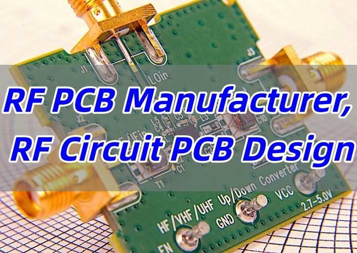
    RF PCB Manufacturer, RF Circuit PCB Design
    Friday, October 17th, 2025

    An ​RF PCB manufacturer​ specializes in creating printed circuit boards for high-frequency applications. This is a field where precision is not just a goal; it is an absolute requirement. This article will guide you through the world of RF circuit boards, from fundamental concepts to advanced manufacturing capabilities.

    Many engineers face significant hurdles when moving from standard PCBs to RF circuit PCB designs. What are the most common pain points?

    • ​Signal Loss and Integrity Issues:​​ The circuit looks perfect on screen, but the real-world performance is poor. Signals weaken or distort across the board, ruining data transmission.
    • ​Impedance Mismatch:​​ Achieving a consistent impedance is incredibly difficult. Even a tiny error in trace width or material thickness can cause signal reflections, degrading performance.
    • ​Heat Management Problems:​​ High-frequency operation generates heat. Standard PCB materials cannot dissipate this effectively, leading to overheating and potential failure.
    • ​Manufacturing Inconsistency:​​ A great design is useless if it cannot be built reliably. Many fabricators lack the tight process controls needed for RF work, leading to frustrating variations from board to board.
    • ​Material Selection Confusion:​​ The range of specialized RF laminates (like Rogers, Taconic, PTFE) is vast. Choosing the wrong material for your application’s frequency and thermal needs is a common and costly mistake.

    Fortunately, these challenges have clear solutions. Partnering with a specialist ​RF PCB manufacturer​ transforms these obstacles into opportunities for optimal performance.

    • ​Precision Engineering:​​ They use advanced simulation software to model signal behavior before production. This ensures the final board maintains excellent signal integrity from input to output.
    • ​Advanced Process Control:​​ They maintain extremely tight tolerances on trace width, spacing, and dielectric thickness. This rigorous control is the only way to guarantee a perfect impedance match.
    • ​Thermal Management Expertise:​​ They understand the thermal properties of specialized materials. They select laminates that effectively dissipate heat and design stack-ups that manage thermal expansion.
    • ​Certified Consistency:​​ A top-tier manufacturer invests in state-of-the-art equipment and rigorous quality certifications like ISO 9001. Every batch meets the same high standard, every time.
    • ​Material Guidance:​​ They act as a consultant. Their engineers help you select the most cost-effective and performance-appropriate RF laminate for your specific project needs.

    At EBest Circuit (Best Technology), we are a specialized ​RF PCB manufacturer​ focused on these exact solutions. Our team thrives on complex, high-frequency challenges. We combine deep material knowledge with cutting-edge fabrication processes to deliver boards that perform as promised. Feel free to contact us at ​sales@bestpcbs.com​ to discuss your project.

    RF PCB Manufacturer, RF Circuit PCB Design

    RF PCB Manufacturer – EBest Circuit (Best Technology)​

    EBest Circuit (Best Technology) is a leading ​RF PCB manufacturer​ with ​19+ years of experience​ in high-frequency printed circuit board fabrication. We specialize in ​RF/microwave PCBs, ​high-speed digital PCBs, and ​hybrid RF-digital designs, offering ​full turnkey solutions​ from design to assembly.

    Our expertise covers ​Rogers, Taconic, and other high-frequency laminates, ensuring optimal signal integrity for ​5G base stations, radar, aerospace, and wireless communication​ applications.

    1. ​RF PCB Materials & Stackups​

    We support a wide range of ​high-frequency materials​ with ​low dielectric loss (Df) and stable Dk:

    • ​Rogers​ (RO4000Âź, RO3000Âź, RT/duroidÂź)
    • ​Taconic​ (TLX, TLY, RF-35)
    • ​Isola​ (IS680, IS410)
    • ​PTFE-based laminates​ (for mmWave applications)
    • ​Hybrid constructions​ (mixing FR4 with RF materials for cost optimization)

    ​Typical Properties:​​

    • ​Dk (Dielectric Constant):​​ 2.2 – 10.2
    • ​Df (Dissipation Factor):​​ 0.001 – 0.004 @ 10GHz
    • ​Copper Foil:​​ Low-profile (≀1”m Ra) for reduced insertion loss

    2. ​RF PCB Fabrication Capabilities​

    ParameterStandard CapabilityAdvanced Capability
    ​Layers​1-32LUp to 50L (rigid-flex)
    ​Line/Space​4/4 mil3/3 mil (HDI)
    ​Min. Hole Size​8 mil4 mil (laser-drilled)
    ​Impedance Control​±10% (>50Ω)±5Ω (≀50Ω)
    ​Surface Finishes​ENIG, OSP, HASLENEPIG, Hard Gold, Immersion Silver

    3. ​RF-Specific Features​

    ✔ ​Controlled Impedance Routing​ (microstrip, stripline, coplanar waveguide)
    ✔ ​Low-Loss Plated Through Holes (PTHs)​​ for RF signal integrity
    ✔ ​Via Shielding & Back-Drilling​ to reduce stub effects
    ✔ ​Embedded Passives​ (resistors, capacitors) for compact RF designs
    ✔ ​High-Precision Laser Cutting​ for RF antenna arrays

    Why Choose EBest Circuit (Best Technology) for RF PCBs?

    ​1. Engineering Expertise​

    • ​Signal Integrity Analysis​ (HyperLynx, ADS)
    • ​EMI/EMC Optimization​ for RF circuits
    • ​Thermal Management Solutions​ (metal-core, thermal vias)

    ​2. Fast Prototyping & Mass Production​

    • ​24-hour rapid prototyping​ for RF designs
    • ​No MOQ restrictions​ (ideal for R&D and low-volume RF projects)
    • ​Full turnkey assembly​ (SMT, RF testing, box build)

    ​3. Quality & Reliability​

    ✅ ​ISO 9001:2015 & IATF 16949 Certified​
    ✅ ​97% On-Time Delivery​ with real-time WIP tracking
    ✅ ​100% Electrical Testing​ (including RF parameter validation)

    In a nutshell, EBest Circuit (Best Technology) provides ​high-performance RF PCBs​ with ​low loss, tight impedance control, and superior signal integrity. Whether for ​5G base stations, satellite communications, or IoT devices, we deliver ​reliable, high-frequency PCBs​ with fast turnaround and competitive pricing. Pls feel free to contact us for your RF PCB requirements!​​

    What Is the Difference Between RF Printed Circuit Board and Normal PCB?

    First, what does RF stand for? It means Radio Frequency. This refers to electromagnetic waves typically ranging from about 3 MHz up to 300 GHz. An RF PCB is designed to carry these high-frequency signals. So, how is it different from a standard PCB used in, for example, a simple toy or a power supply? The difference is profound.

    Think of it like this: a normal PCB is like a local road. It handles traffic moving at slower speeds. An RF PCB is like a Formula 1 racetrack. It is engineered for incredible speed and precision. Even the smallest bump or imperfection can cause a disaster.

    Here are the three key distinctions:

    1. ​The Core Material:​​ Standard PCBs often use FR-4, a glass-reinforced epoxy laminate. It is a great general-purpose material. However, for RF signals, FR-4 has a high “loss tangent.” It absorbs signal energy, turning it into heat. RF PCBs use low-loss laminates like PTFE or ceramic-filled hydrocarbons. These materials allow the signal to pass through with minimal loss.
    2. ​The Importance of Impedance:​​ In standard digital boards, impedance control is often less critical. In RF work, it is everything. Every trace must be precisely calculated and fabricated to maintain a specific characteristic impedance (usually 50 or 75 ohms). This prevents signal reflections and ensures maximum power transfer.
    3. ​The Design Philosophy:​​ RF circuit PCB design requires accounting for electromagnetic effects that are negligible at lower frequencies. Aspects like skin effect (where current flows only on the conductor’s surface) and parasitic capacitance/inductance become dominant factors. The layout is not just about connecting points; it is about shaping the electromagnetic field.

    In short, while all PCBs provide electrical connections, an RF PCB is a carefully tuned component in itself. Its material, layout, and manufacturing are all optimized for guiding high-frequency energy efficiently.

    What Is RF PCB Material?

    The foundation of any high-performance RF board is its material. RF PCB material is a specialized laminate designed to excel in high-frequency environments. The right choice directly determines the board’s loss, thermal stability, and reliability.

    Key properties define a good RF material:

    • ​Dielectric Constant (Dk):​​ This measures how much the material “slows down” an electrical signal. A stable Dk is crucial. If it varies with frequency or temperature, your impedance will be unpredictable. RF materials have a tight Dk tolerance.
    • ​Dissipation Factor (Df) or Loss Tangent:​​ This is perhaps the most critical property. It indicates how much signal energy is lost as heat. A lower Df value means less signal loss. RF materials have an extremely low loss tangent compared to FR-4.
    • ​Thermal Coefficient of Dk:​​ This tells you how much the Dk changes with temperature. A low value means your circuit’s performance remains stable even as it heats up.
    • ​Coefficient of Thermal Expansion (CTE):​​ Materials expand when heated. A CTE that closely matches that of copper is vital. A mismatch can cause broken connections or delamination during assembly or operation.

    Common materials used by an ​RF laminate PCB manufacturer​ include PTFE (Teflon¼), ceramics, and specialized hydrocarbon resins. Brands like Rogers, Taconic, and Arlon are industry leaders. Selecting the right one is a balance of performance, cost, and manufacturability. This is where an experienced ​RF PCB manufacturer in China​ or elsewhere can provide invaluable guidance.

    What Is RF Circuit PCB Design?

    RF circuit PCB design refers to the process of designing printed circuit boards that handle signals in the radio frequency range, typically above 30 MHz. These boards serve as the physical platform for amplifiers, antennas, mixers, and oscillators used in wireless systems.

    The primary goal is to preserve signal integrity while reducing loss and unwanted coupling. Unlike low-frequency designs, where DC resistance dominates, RF design must account for distributed parameters—inductance (L) and capacitance (C)—that vary along the trace.

    The characteristic impedance Z0 is central to RF PCB design, defined as:

    RF PCB Manufacturer, RF Circuit PCB Design

    A mismatch between source and load impedances leads to reflections, quantified by the reflection coefficient:

    RF PCB Manufacturer, RF Circuit PCB Design

    Where ZL is the load impedance. To minimize reflections and achieve efficient power transfer, ZL must closely match Z0, usually 50 Ω for most RF systems.

    Key Design Principles of RF PCBs

    Controlled Impedance Design

    Every RF trace functions as a transmission line, not just a conductor. The impedance depends on geometry and dielectric properties. For microstrip structures, the impedance is approximated by:

    RF PCB Manufacturer, RF Circuit PCB Design

    where:

    • (h): dielectric height,
    • (w): trace width,
    • (t): copper thickness,
    • Δr: dielectric constant.

    A deviation of even ±10% from the target impedance can distort RF signals, increasing insertion loss and reflection.

    Impedance Matching

    Impedance matching ensures maximum power transfer between circuit stages. When mismatch occurs, reflected energy travels back to the source, forming standing waves. The relationship between reflection coefficient and Voltage Standing Wave Ratio (VSWR) is:

    RF PCB Manufacturer, RF Circuit PCB Design

    In practice, designers use Smith charts, stub tuners, or LC matching networks to visualize and optimize matching.

    Transmission Line Effects

    At RF frequencies, traces behave like distributed elements rather than lumped components. Propagation delay, attenuation, and coupling must be analyzed using electromagnetic simulation. The wavelength λ is given by:

    RF PCB Manufacturer, RF Circuit PCB Design

    where (c) is the speed of light, (f) the frequency, and Δeff​ the effective dielectric constant.

    Material Selection for RF PCB

    The choice of substrate determines dielectric stability and signal loss.

    MaterialDielectric Constant (Δr)Loss Tangent (tanΎ)Frequency StabilityTypical Use
    FR-44.2–4.70.02Poor above 1 GHzLow-cost applications
    Rogers RO4350B3.480.0037Excellent up to 10 GHzRF amplifiers, filters
    PTFE (Teflon)2.10.0009Outstanding up to 30 GHzAerospace, radar systems

    Key considerations:

    • Lower tanÎŽ means lower dielectric loss.
    • Stable Δr​ ensures consistent impedance.
    • Surface roughness of copper affects conductor loss, especially at GHz frequencies.

    PCB Stack-up and Geometry

    RF designs usually adopt multilayer stack-ups to separate high-frequency and control layers. A common four-layer configuration might include:

    1. Top Layer – RF signal traces
    2. Inner Layer 1 – Solid ground plane
    3. Inner Layer 2 – Power plane
    4. Bottom Layer – Control and bias circuits

    Proper ground referencing is vital. The return path should be directly beneath the signal line to maintain uniform impedance. Vias must be minimized or placed symmetrically to prevent inductive discontinuities.

    Differential routing is used for balanced RF lines (e.g., antennas or mixers). The differential impedance Zdiff is roughly:

    RF PCB Manufacturer, RF Circuit PCB Design

    where (s) is the spacing between differential traces.

    Layout and Routing Techniques

    Minimizing Coupling and Crosstalk

    Keep high-power and low-power RF paths separated. Perpendicular routing between layers reduces unwanted coupling.

    Shielding Methods

    Use guard traces and via fences around sensitive lines. Stitching vias at 1/20th wavelength intervals confine electromagnetic fields effectively.

    Return Path Optimization

    Ensure ground continuity with via stitching near corners or component pads. Avoid long current loops that may radiate noise.

    Simulation and Testing in RF PCB Design

    RF verification relies on both simulation and measurement.

    • S-Parameter Analysis:
      • S11: Return loss (input reflection).
      • S21: Insertion loss (forward transmission).
      • Ideal design targets:
        • S11< -10 dB)
        • S21 > -3 dB)

    The Return Loss formula is:

    RF PCB Manufacturer, RF Circuit PCB Design
    • Time Domain Reflectometry (TDR): Detects impedance discontinuities along traces.
    • Network Analyzer Testing: Validates gain, phase shift, and bandwidth performance.

    Accurate measurement ensures the PCB meets design specifications before mass production.

    Applications of RF Circuit PCB

    RF PCBs are embedded in numerous systems:

    • Wireless communication modules (Wi-Fi, Bluetooth, LTE)
    • IoT sensors and gateways
    • Automotive radar and collision avoidance systems
    • Satellite and aerospace communication
    • Medical telemetry and imaging devices

    As the world transitions to 5G and beyond, RF PCB design has become central to achieving higher data rates and stable wireless connections.

    Technical Capability for RF PCB Manufacturer

    At EBest Circuit (Best Technology), our RF PCB manufacturing capabilities are built on nearly two decades of specialized experience in high-frequency circuit fabrication. We combine state-of-the-art equipment with rigorous quality control processes to deliver PCBs that meet the demanding requirements of modern RF applications, from 5G infrastructure to aerospace systems.

    ​1. Precision Manufacturing with Advanced Equipment​

    • ​Laser Direct Imaging (LDI)​​
      • Min. trace/space: ​3/3 mil (standard) → 1/1 mil (advanced)​​
      • Copper thickness: Inner layers (HOZ-20OZ) | Outer layers (1OZ-20OZ)
    • ​Plasma Etching Systems​
      • Critical for RF signal integrity, supports ​10:1 aspect ratio microvias​ and ​0.15mm ultra-fine holes​

    ​2. Rigorous RF Performance Validation​

    • ​40GHz Network Analyzers​
      • Direct measurement of insertion loss/return loss up to ​40GHz​
    • ​Time-Domain Reflectometry (TDR)​​
      • Full-path impedance control: ​​±5% (standard) | ±3% (advanced)​​
    • ​Material Characterization​
      • ​Dk/Df testing​ for Rogers, Taconic, and other high-frequency laminates

    ​3. RF-Optimized Material Portfolio​

    ​Material Class​​Standard Options​​High-Frequency Solutions​
    FR4KB6165 (TG150)Isola 370HR, FR408HR
    High-Frequency Laminates–Rogers 4350/5880, Taconic TLY-5
    Ultra-Low Loss Materials–Nelco N4000-13, PTFE-based substrates
    ​Dielectric Layers​1080/2116/7628 PPUltra-thin cores (0.1mm, copperless)

    ​4. Key Process Capabilities​

    • ​Impedance Control​
      • Inner layers (1OZ): ±5% (4/4mil) → ​​±3% (3/3mil)​​
    • ​High-Frequency Surface Finishes​
      • ENIG (Ni 3-8ÎŒm | Au 0.025-0.125ÎŒm) for ​mmWave applications​
      • Electroless NiPdAu (Pd 0.05-0.125ÎŒm) for superior solderability

    ​5. Multilayer RF PCB Expertise​

    • ​Layer Stack-Up: 1-32 layers (High-TG mandatory for 8+ layers)
    • ​Thickness Control:
      • Ultra-thin: ​0.15mm±0.05mm​ (ENIG only)
      • Thick-board: ​8.0mm​ (special back-drilling)
    • ​Hybrid Construction: FR4 + Rogers material combinations

    ​6. Scalable Production & Fast Turnkey​

    • ​Max. Panel Size: 1980mm (single/double-sided) | 750mm (multilayer)
    • ​High-Mix Flexibility:
      • Supports ​2,000pcs/batch​ for ultra-small boards (<0.0004mÂČ)

    7. Design Support Services​

    • DFM (Design for Manufacturing) analysis for RF layouts
    • Signal integrity and thermal management consulting
    • Material selection guidance based on application requirements
    • Rapid prototyping with engineering feedback within 24 hours

    Through continuous investment in advanced equipment and process optimization, EBest Circuit (Best Technology) maintains its position as a leading RF PCB manufacturer capable of meeting the most demanding high-frequency application requirements.

    How Do RF Laminate PCB Manufacturers Ensure Quality?

    Quality in RF manufacturing is not an afterthought. It is integrated into every step. For an ​RF laminate PCB manufacturer, ensuring quality means controlling every variable that could affect the final electrical performance. The process is meticulous.

    1. ​Incoming Material Inspection:​​ It starts with the raw laminate. We verify the dielectric thickness and copper cladding weight against specifications. Using a material with the wrong Dk will ruin the entire batch.
    2. ​Process Control During Fabrication:​​ We constantly monitor critical parameters. Etching chemistry, lamination pressure and temperature, and plating thickness are all tightly controlled. This consistency is key to achieving the designed impedance.
    3. ​Electrical Testing:​​ 100% of our RF boards undergo electrical testing. We use fixtures to test for continuity (no shorts or opens). More importantly, we sample-test boards for high-frequency parameters like impedance and loss, ensuring they meet the customer’s data sheet.
    4. ​Microsection Analysis:​​ We regularly cross-section sample boards. This allows us to physically measure critical features: trace width, dielectric thickness, and plating quality. This data confirms our processes are in control.

    This systematic approach separates a true specialist from a general-purpose fabricator. It is how we guarantee that the board you receive will perform exactly like the one you designed.

    How to Select RF PCB Manufacturers?

    Choosing the right partner is critical. Your ​RF PCB design​’s success depends on their skill. Here is a simple checklist to help you select an ​RF PCB manufacturer.

    • ​Proven Experience:​​ Ask for examples of previous work. A good ​RF microwave PCB manufacturer​ will have a portfolio of projects similar to yours.
    • ​Technical Questions:​​ Gauge their expertise. Ask them how they control impedance or which materials they recommend for your frequency band. Their answers will reveal their depth of knowledge.
    • ​Quality Certifications:​​ Look for ISO 9001 certification. This shows a commitment to a documented quality management system.
    • ​Testing Capabilities:​​ Ensure they have the necessary equipment to verify RF performance, not just basic connectivity.
    • ​Communication and Support:​​ You need a responsive partner. Choose a manufacturer that assigns a dedicated engineer to your project for clear and technical communication.

    Whether you are looking for an ​RF PCB manufacturer in the USA, China, or Europe, these core criteria remain the same. The goal is to find a partner, not just a supplier.

    Case Study: RF Microwave PCB Board Manufacture by EBest Circuit (Best Technology)​

    ​Challenge: High-Frequency Signal Integrity​

    A 5G base station OEM required ​24-layer RF microwave PCBs​ with:

    • ​Strict impedance control​ (±3%) for 28GHz mmWave signals
    • ​Low-loss laminate​ (Df <0.004) to minimize attenuation
    • ​Plated through-holes (PTH) with 10:1 aspect ratio​ for dense interconnects

    ​Our Manufacturing Solution​

    1. ​Material Expertise:
      • Selected ​Rogers 5880​ (Dk=2.2, Df=0.0009) for critical RF layers
      • Hybrid stack-up with ​FR408HR​ for cost-sensitive digital layers
    2. ​Advanced Processes:
      • ​Laser-drilled microvias​ (0.10mm) + ​plasma desmear​ for void-free plating
      • ​3/3 mil trace/space​ with ±2ÎŒm alignment tolerance (LDI technology)
    3. ​Quality Validation:
      • ​40GHz network analyzer​ confirmed insertion loss <0.15dB/inch
      • ​100% TDR testing​ ensured impedance consistency across panels

    ​EBest Circuit (Best Technology)’s RF Microwave PCB Capabilities​

    ◼ ​Materials: Rogers, Taconic, Isola, Nelco, PTFE, and hybrid FR4 options
    ◼ ​Critical Tolerances:

    • Line width/spacing: ​1/1 mil​ (special process)
    • Hole size: ​0.10mm (laser)​​ | ​0.15mm (mechanical)​​
    • Impedance control: ​​±3%​​ (standard), ​​±2%​​ (advanced)
      ◼ ​Testing:
    • 40GHz RF performance validation
    • TDR, thermal cycling, IST (interconnect stress testing)
      ◼ ​Applications: 5G mmWave, satellite comms, radar, medical RF devices

    In conclusion, an ​RF PCB manufacturer​ bridges the gap between high-frequency theory and real-world application. This article has explored the critical aspects that define quality in RF circuit board production. From material science to precision manufacturing, each step is vital for success.

    At EBest Circuit (Best Technology), we are passionate about tackling complex RF and microwave challenges. Our expertise in ​RF circuit PCB design​ and manufacturing ensures your project is built to the highest standards. We are committed to being your reliable partner. Pls contact our team of experts at ​sales@bestpcbs.com for RF PCB manufacturing supports.

    You may also like

    RF Printed Circuit Board, RF PCB Manufacturer, Fast Turnkey Service
    Wednesday, June 4th, 2025

    RF printed circuit board is widely used in wireless systems, communication infrastructure, and advanced radar equipment. These boards need tight control over signal paths and impedance to prevent performance issues. At EBest Circuit (Best Technology), we focus on delivering top-quality RF PCBs with full technical support and fast turnkey service.

    EBest Circuit (Best Technology) is an R&D-driven RF PCB manufacturer, offering RF printed circuit board prototype, design, and assembly services. Our factory abides by ISO 9001, ISO 13485, IATF 16949, and AS9100D for every manufacturing process.  Our engineers are knowledgeable about RF printed circuit board design and adhere to the highest standards of professionalism. If any RF printed circuit board projects, just feel free to let us know at sales@bestpcbs.com at any moment.

    RF Printed Circuit Board

    What is RF Printed Circuit Board?

    RF printed circuit board, short for radio frequency printed circuit board, is designed to handle signals in the megahertz to gigahertz range. These boards work in high-frequency environments where even minor signal losses or noise can harm system performance. Standard PCBs can’t manage such challenges, so RF PCBs follow different design and material rules.

    RF PCB Manufacturer, Fast Turnkey Service

    What is PCB Material for RF Printed Circuit Board?

    Material choice is key to performance. Common RF PCB materials include Rogers RO4350, Teflon, and PyraluxÂź AP. These have low dielectric constant (Dk) and low dissipation factor (Df), which means lower signal loss. Unlike FR-4, RF-grade materials are stable over frequency and temperature. This stability ensures clear signals even in harsh environments.

    What are the RF Traces on a RF Printed Circuit Board?

    RF traces are signal paths that need exact width, spacing, and length control. They carry sensitive signals that can reflect or lose energy if routing is not precise. Microstrip and stripline are two common trace styles. Engineers also use 45° angles and matched lengths for differential pairs to avoid signal mismatches and reduce interference.

    How Thick is a RF Printed Circuit Board?

    RF PCBs come in many thicknesses, but the choice depends on frequency, stack-up, and design needs. Typical boards are between 0.4mm and 3.2mm. ‌Some high-frequency applications‌ require thinner layers and tight stack-up tolerance. Layer-to-layer alignment must also be precise—within ±10ÎŒm—to reduce signal loss during travel.

    What is RF Printed Circuit Board Design?

    RF PCB design is much more than layout. It includes trace width calculation, layer stack-up, EMI shielding, grounding, and impedance control. Decoupling capacitors and shielding cans help reduce noise. Design rules also avoid sharp angles and encourage short, direct routing. At EBest Circuit (Best Technology), we support design analysis to prevent issues early.

    How to Make an RF Printed Circuit Board?

    Making an RF PCB involves several advanced steps:

    1. Material prep and layer alignment
    2. High-precision laser drilling
    3. Impedance-controlled trace etching
    4. Multi-layer lamination with ±10Όm accuracy
    5. Plating with surface roughness below 0.5ÎŒm
    6. Final testing including TDR, VNA, and EMC

    These steps ensure high signal integrity. At EBest Circuit (Best Technology), we also offer 24-72 hour quick-turn services to reduce your time to market. For urgent projects, we prioritize production and testing.

    What is RF Printed Circuit Board Used For?

    RF PCBs serve many industries:

    • 5G base stations
    • Radar systems
    • Satellite communication
    • Medical imaging
    • IoT modules and RF modules

    These applications need high reliability. A small error can impact performance. That’s why choosing the right manufacturer is critical.

    Why Choose EBest Circuit (Best Technology) as Your RF PCB Manufacturer?

    Many clients face issues like poor signal integrity, delayed delivery, or high cost. At EBest Circuit (Best Technology), we understand these challenges. That’s why we offer:

    • Fast Turnaround: 24–72 hour quick-turn service to help speed up your launch.
    • Design Support: Full assistance from layout review to final testing. We help reduce EMI and ensure impedance accuracy.
    • Cost Optimization: Efficient material usage, smart supply chain, and process control cut waste and save money.

    We also follow strict design rules for high-frequency applications. These include:

    • Use of matched differential pairs
    • Short, direct signal paths with no 90° turns
    • Use of decoupling capacitors and ground shielding
    • Accurate impedance matching using simulation tools
    RF PCB Manufacturer

    All in all, EBest Circuit (Best Technology) provides RF PCB manufacturing with quality, speed, and support. We help you avoid crosstalk, mismatched impedance, and long prototype cycles. With our experience, tools, and team, you can go to market faster. Whether you’re building IoT modules or 5G routers, we’ll help you meet your RF performance goals—on time and on budget. Reach out to us at sales@bestpcbs.com to start your RF PCB project.

    You may also like

    RF PCB Manufacturer, RF PCB Manufacturing​
    Monday, April 7th, 2025

    RF PCB manufacturer is a term often searched by engineers and businesses looking for high-quality, high-frequency printed circuit boards. In today’s fast-paced tech world, signal strength, low loss, and stable performance are non-negotiable. Whether you are creating 5G devices or aerospace modules, having the right partner in RF PCB fabrication is crucial. Let’s explore what goes into this process, how materials matter, and why the manufacturer you choose make a difference.

    EBest Circuit (Best Technology) is one of the leading RF PCB manufacturers in China, specializing in RF PCB fabrication, RF PCB design, and multilayer RF PCB manufacturing. EBest Circuit (Best Technology) used high-quality RF PCB materials, such as Rogers RO4350, RO4003, and PTFE (DuPont Teflon). We believe quality is the first. If you are looking for a reliable RF PCB manufacturer, just don’t hesitate to choose EBest Circuit (Best Technology) as your partner. Feel free to contact us at sales@bestpcbs.com.

    RF PCB Manufacturer, RF PCB Manufacturing​

    What is RF PCB Manufacturing?

    RF PCB manufacturing refers to the process of building circuit boards that handle high-frequency signals. Unlike standard boards, these work at frequencies from hundreds of MHz to several GHz. Every step, from design to final assembly, must reduce signal loss, noise, and interference. This makes the process more specialized compared to regular PCB production.

    The job of an RF PCB manufacturer is to build boards that transmit data with speed and clarity. These boards are used in wireless communication, radar, satellite, and medical systems. The RF signal paths need careful design, tight control of dimensions, and excellent copper surface finishes.

    What Are the RF PCB Material?

    Material choice is a critical factor. Good materials reduce signal loss and support stable signal transmission. Common materials used by experienced RF PCB manufacturers include:

    • Rogers 4350B: Offers low dielectric loss and stable performance.
    • Taconic RF-35: Preferred for its cost-effectiveness and stable frequency behavior.
    • Teflon (PTFE): Great for very high-frequency applications but harder to process.
    • FR4 (for mixed designs): Sometimes used with other high-end substrates in hybrid boards.

    Choosing the right RF PCB material ensures high signal integrity, low insertion loss, and better impedance control. A reliable RF circuit board manufacturer will offer a variety of materials based on your project’s frequency range and power levels.

    How is a PCB Manufactured?

    While every PCB shares some basic steps, RF PCB fabrication includes extra precision:

    • Design & Layout: Engineers define the RF path, stackup, and signal traces.
    • Material Preparation: Boards are prepared using selected RF PCB materials.
    • Lamination: Layers are pressed under heat and pressure.
    • Drilling: High-precision equipment drills clean and accurate holes.
    • Plating: Holes and surface areas are plated with copper.
    • Imaging: Photolithography transfers the circuit image onto copper.
    • Etching: Removes unwanted copper, leaving only the designed circuit.
    • Surface Finish: ENIG or silver is applied for better conductivity.
    • Inspection: AOI, X-ray, and other tests ensure the board meets specs.

    Every step affects the RF performance, especially in multilayer RF PCB manufacturing.

    RF PCB Manufacturer

    What Makes a Reliable RF PCB Manufacturer Stand Out?

    Finding the right partner is more than just checking price. A reliable RF PCB manufacturer offers:

    • Experience with high-frequency designs
    • Strong control over materials and processes
    • Advanced equipment for small trace width and spacing
    • Quick turnaround and flexible volumes
    • Full-service PCB express and assembly support
    • Consistent quality and long-term reliability

    Top-tier RF PCB manufacturers also provide help with design tweaks, stackup consulting, and thermal management suggestions. These extras help avoid problems before they occur.

    Where to Find an Experienced RF PCB Manufacturer in China?

    China is a hub for circuit board manufacturing companies, but not all can handle RF PCB boards. Below is the sourcing Strategies‌:

    • ‌Industry Networks‌: Engage with trade platforms like ‌Global Sources‌ or ‌Alibaba‌ (filter for RF PCB specialists with verified reviews).
    • ‌Trade Shows‌: Attend ‌China Electronics Fair (CEF)‌ or ‌HK Electronics Fair‌ to meet manufacturers and review RF-focused innovations.
    • Focus on the technology-driven areas known for RF PCB excellence: Shenzhen renowned for its leadership in electronics research, development, and manufacturing. The city hosts a concentration of specialized manufacturers with deep expertise in processing advanced high-frequency materials such as ‌Rogers, Taconic, and PTFE‌, making it a prime destination for cutting-edge RF PCB production.

    Finally, look for companies that:

    • Specialize in RF and microwave PCB board manufacture
    • Have a history of international projects
    • Offer quick response and English-speaking support
    • Follow IPC and ISO quality standards

    EBest Circuit (Best Technology) is a professional RF printed circuit board manufacturer. With more than 18 years of focus in this niche, we offer design support, fabrication, and PCB assembly services all under one roof.

    How to Choose RF PCB Manufacturers?

    Selecting an RF PCB manufacturer requires a checklist. Here are key things to consider:

    • Materials: Can they source and work with high-frequency materials?
    • Design Review: Do they offer suggestions on improving performance?
    • Stacking and Stackup Options: Can they handle complex PCB stacking?
    • Equipment: Do they use laser direct imaging (LDI) and high-accuracy drilling?
    • Testing: Are they doing RF-specific tests like impedance or insertion loss?
    • Customization: Can they support MMCX, SMA, or other RF PCB connectors?

    Avoid working with companies that don’t provide complete transparency. Ask questions, request RF PCB prototypes, and check their certifications.

    RF PCB Manufacturing​

    Why Should You Choose EBest Circuit (Best Technology) as Your RF PCB Manufacturer?

    EBest Circuit (Best Technology) is not just another RF PCB manufacturer in China. Here’s why they are a strong choice:

    • Specialized in high-frequency PCB fabrication for 18+ years: EBest Circuit (Best Technology) has provided high-quality RF PCB products continually since 2006. The max panel size in EBest Circuit (Best Technology) supports up to 600*500mm (23.62″*19.68″). The turnaround time for samples is 7-9 days, and mass production orders take approximately 8 days.
    • In-house support for RF PCB design and material selection: The RF PCB fabrication process and other manufacturing processes are more complex than FR4, so need unique handling methods and experienced workers. EBest Circuit (Best Technology) has a strong R&D team to optimize RF PCB design and a professional procurement team to control the supply chain material costs without compromising the material quality.
    • Flexible options including rigid PCB, multilayer RF boards, and hybrid stack-ups: EBest Circuit (Best Technology) provides manufacturing and sale service of various types of RF printed circuit boards and assembly. All our RF PCB products are fully customizable to meet your exact design and application requirements. The technical expertise in EBest Circuit (Best Technology) covers advanced materials like Rogers and PTFE, with strict adherence to IPC and ISO standards for precision and reliability.
    • Advanced testing methods ensure your board performs as expected: EBest Circuit (Best Technology) is a direct RF PCB manufacturer. We have SMT factories in China and Vietnam respectively. ISO quality standard was applied to each step from RF PCB raw material purchasing, RF PCB production, inspection, and packing, to sales and marketing. Using the latest technology and high-tech production equipment, EBest Circuit (Best Technology) continuously improves the production process, test and measurement technology, and optimizes the quality management system.
    • Reliable delivery with express PCB service for urgent orders: EBest Circuit (Best Technology) prioritizes customer satisfaction above all. We are committed to providing more efficient service to customers and going to be one of the most reliable partners in China. Should you require urgent order coordination, please communicate directly with our team. EBest Circuit (Best Technology) will try every means to suit your needs.
    • Expertise in RF connectors, including MMCX and SMA mounting: We are able to manufacture the RF PCB with RF PCB connectors according to the design files of the customers. Technical support like material selection, impedance calculation, high-frequency testing, impedance testing, and VNA (Vector Network Analyzer) verification will be provided.

    EBest Circuit (Best Technology) caters to a global clientele of over 1,700 customers spanning more than 40 countries. Customers come back not just because of quality, but because EBest Circuit (Best Technology) helps reduce design risk, cut lead times, and simplify complex builds.

    RF PCB Manufacturer

    In conclusion, working with the right RF PCB manufacturer makes a difference from the very start. From choosing the best materials to building boards that can handle today’s demanding signal speeds, it takes knowledge and precision. Whether you are in telecom, aerospace, automotive radar, or defense, a reliable RF PCB partner saves time, cost, and headaches.

    EBest Circuit (Best Technology) offers the full package like design support, quality production, and fast delivery. For your next RF project, we are a manufacturer you can trust. Our goal is to provide customers defect defect-free RF PCB products fully consistent with their requirements to ensure each part presented to customers has top excellent quality. With strong service and deep expertise, your ideas can move from RF PCB concept to reality without quality compromise. For more about RF PCB fabrication or to request a fast quote, pls feel free to contact our sales engineer team at sales@bestpcbs.com.

    You may also like