If you need a high frequency PCB in Switzerland, first determine where the board will be manufactured and whether that factory can process the specified laminate, stackup, impedance, and RF test requirements. The suppliers below cover Swiss production, European production, a Swiss sourcing office, and overseas manufacturing, so compare quotations by the proposed factory and scope rather than the company address alone.
This article gives you 10 suppliers to approach, explains how to use the list, and compares Swiss, European, and overseas sourcing. It also shows which RF capabilities, materials, stackup data, impedance limits, tests, files, and DFM answers to request before you compare quotations and approve production.

10 High Frequency PCB Suppliers to Consider for Projects in Switzerland
Start with these 10 suppliers, then narrow the list by manufacturing site, laminate experience, stackup fit, and available RF verification. Their supply models differ, so each quotation should identify where the board will be made and which site owns the RF process.
1. Optiprint AG, Switzerland
Optiprint provides a Swiss-manufacturing option from its Berneck operation. The company publishes high-frequency and PTFE PCB capability for Rogers, Taconic, and Neltec materials, mixed-dielectric multilayers, and metal-core or metal-backed constructions. Include it in the RFQ when Swiss manufacture, direct local engineering contact, or a specialized PTFE construction is part of the sourcing requirement.
2. Fineline Switzerland AG
Fineline has a Swiss office in Lucerne and publishes RF PCB capability through a global network of audited manufacturing partners, including materials and constructions for frequencies up to 100 GHz. This is a sourcing and engineering route rather than proof of a Swiss factory. Ask the Swiss team to name the proposed plant, material source, test scope, and subcontracted operations before adding the offer to a factory-level comparison.
3. ACB, France
ACB publishes a dedicated RF and microwave PCB service supported by its French manufacturing operation. Its public information covers PTFE-based materials, hybrid constructions, multilayer RF boards, and work for microwave applications. Ask ACB to quote when the design needs a European RF specialist, then confirm the exact plant, laminate availability, and board-specific schedule during RFQ review.
4. Aspocomp, Finland
Aspocomp manufactures in Oulu and publishes high-frequency multilayer, PTFE, mixed-build, and HDI capability. That combination is useful when an RF section must coexist with microvias, dense interconnects, or a mixed RF/FR-4 construction. Public delivery information does not replace a stackup-specific schedule; the quotation still needs to tie material availability and timing to the proposed build.
5. AT&S, Austria
AT&S lists high-frequency PCBs up to 10 layers at its Fehring plant in Austria, alongside standard multilayer, HDI, flexible, semi-flexible, and rigid-flex technologies. This makes the site relevant when RF requirements sit inside a broader interconnect problem. The RFQ should name Fehring or another approved build site explicitly, because group capability should not be assumed to apply at every AT&S location.
6. Eurocircuits, Europe
Eurocircuits offers an RF Pool route for eligible 2- and 4-layer boards using I-Tera and Rogers materials, plus non-pooled options for other constructions. Its model is suited to prototypes and small quantities that fit a defined online manufacturing envelope, with manufacturability checking and electrical test included in that service. Designs outside the published envelope should be treated as a separate engineering quotation rather than forced into the pooled route.
7. KSG, Germany and Austria
KSG publishes high-frequency PCB production for 24 to 77 GHz applications, with 2 to 20 layers, PTFE and hydrocarbon materials, and homogeneous or hybrid multilayers. The capability is relevant to radar, sensing, and other designs in which etching control and material choice directly affect RF geometry. Buyers should still confirm which KSG factory will build the board and which combinations of material, layer count, thickness, and tolerance are available together.
8. Schweizer Electronic, Germany
Schweizer Electronic publishes RF technology paths for 6-24 GHz and 77 GHz and operates PCB production in Schramberg, Germany. Its profile is particularly relevant to radar and sensor programs that need high-frequency structures within an established European production route. Because the group also has manufacturing outside Germany, the quote should state the actual production and qualification site.
9. Teledyne Labtech, United Kingdom
Teledyne Labtech manufactures complex RF and microwave PCBs in the UK and publishes PTFE, LCP, mixed-dielectric, multilayer, metal-backed, and thermally managed constructions. It also offers assembly and RF test services, with an accelerated option for qualifying prototypes. Ask it to quote when the project needs specialist microwave fabrication or a closer link between bare-board manufacture, assembly, and RF verification.
10. EBest Circuit, China
EBest Circuit is a China-based PCB manufacturer supplying international projects, including deliveries to Switzerland. Published capabilities include Rogers and PTFE materials, Rogers/FR-4 hybrid constructions, controlled-impedance fabrication, prototypes, and production support. EBest Circuit does not claim a factory, warehouse, or branch in Switzerland, so buyers should evaluate it as an overseas manufacturing route and define the import and delivery boundary in the RFQ.
Before moving a supplier to the next round, obtain written confirmation of the manufacturing site, material, construction, test scope, quantity, and schedule. A capability page is enough to start the conversation, but the quotation must answer these project-specific points.
How Should You Use This Supplier List for Your RFQ?
Use the ten names as a first-round candidate pool, then send the same technical package to every supplier. A company should advance only if its reply connects your files to an identified factory, a buildable stackup, available material, and a defined verification plan.
- Confirm the build site: ask for the legal entity, factory address, subcontracted processes, inspection location, and ship-from country.
- Confirm material availability: request the exact laminate, bondply or prepreg, thickness, copper type, and any minimum buy or procurement delay.
- Request a proposed stackup: compare dielectric thicknesses, reference planes, finished copper, RF layers, and all deviations from the supplied construction.
- Define verification: state the impedance coupon, sampling, RF measurements, dimensional checks, raw data, and report format required for acceptance.
- Match the production stage: separate prototype quantity, qualification lot, repeat order, and forecast volume instead of assuming one route fits all four.
- Lock changes: require customer approval before a material, dielectric thickness, copper type, RF geometry, test method, or production site is changed.
A useful first-round response should expose open assumptions rather than hide them behind a unit price. Remove any candidate that cannot identify the factory or return a construction that can be checked against the RF requirements.
Should You Source High Frequency PCBs Locally or Overseas?
Choose the production region from the project requirement, not from a general belief that one country is always better. The correct route depends on contractual origin, engineering access, process fit, material supply, quantity, logistics, and the cost of qualifying a second site.
Switzerland-based manufacturing makes sense when the contract requires Swiss manufacture, the project needs close access to the production team, or the RF construction is available from a qualified Swiss plant. The RFQ should identify which operations must occur in Switzerland instead of accepting a Swiss invoice or sales address as proof of origin.
European manufacturing can provide a regional factory and shorter transport path while expanding the available RF process base. It suits projects that do not require Swiss-made boards but still want production within Europe. Check the actual plant, because a European sales or engineering office can still route work to a different country.
Overseas manufacturing is practical when the contract permits it and the supplier can return a complete digital engineering package. It may expand material, capacity, and commercial options, but the Swiss buyer must define importing, customs clearance, Incoterms, document ownership, nonconformance returns, and the approval required for any site transfer.
Location is one qualification field, not a substitute for technical review. Select the route that can meet the approved RF baseline and make its responsibilities clear from factory release through arrival in Switzerland.
Which High Frequency PCB Capabilities Should You Confirm First?
Confirm whether the proposed factory can manufacture the exact RF structure before discussing general company credentials. The answer should refer to a named site and to combinations that have been reviewed against your layer count, materials, geometry, and panel design.
- Low-loss laminate processing: verify the named PTFE, hydrocarbon-ceramic, LCP, or other RF material family and the related drilling, plasma, plating, bonding, and surface-preparation route.
- Mixed-dielectric multilayers: ask whether the factory can press the proposed RF material with FR-4 or another dielectric while holding the required finished thickness and registration.
- Controlled-impedance fabrication: confirm field-solver review, coupon design, etching compensation, dielectric control, finished copper assumptions, and access to TDR data.
- RF via structures: identify plated-through vias, blind or buried vias, via filling, via fences, backdrilling, and the residual-stub limit that the design requires.
- Special mechanical construction: confirm cavities, metal-backed boards, coins, edge plating, depth routing, thin dielectrics, or oversized panels only when the drawing calls for them.
- Registration and conductor control: ask for the achievable result for the proposed material and copper, not an isolated minimum trace value copied from a general capability table.
“We make RF PCBs” is not enough. The factory should either confirm the requested combination or return the limits and changes needed to make it manufacturable.
What RF Materials and Stackup Details Should Be Included in the RFQ?
Name the exact material system and define the finished construction that the electrical design assumes. “Rogers PCB” or “low-loss material” leaves too many variables open for suppliers to quote the same board.
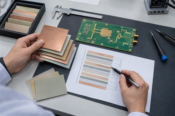
- Laminate and bonding materials: manufacturer, product family, grade, core, bondply or prepreg, and approved source where the project controls it.
- Electrical values: the Dk and Df used in design, including the data source, test method, frequency, direction, and whether the value is a design or process value.
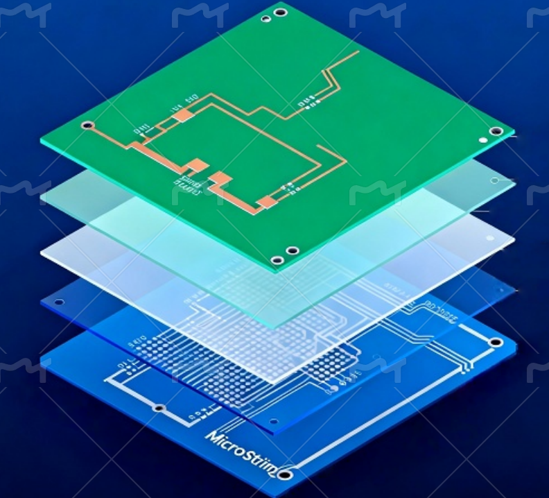
- Finished stackup: layer order, RF signal layers, reference planes, finished dielectric thicknesses, total thickness, and tolerance.
- Copper definition: foil type or profile where relevant, starting copper, plating contribution, and required finished copper on each controlled layer.
- Hybrid construction: the location of each RF and conventional material, bonding system, resin constraints, and any special sequential lamination.
- Substitution rule: the parameters that must remain equivalent and the written approval required before any alternate material is used.
Ask every bidder to return its proposed stackup with the quotation. This exposes material or thickness substitutions before they become hidden differences in impedance, loss, phase, or lead time.
How Should Controlled Impedance and RF Performance Be Specified?
Specify the electrical result separately from the method used to test it. The fabrication drawing and RF requirement should say what the board must achieve; the inspection plan can then define how that result will be verified.
- Impedance: list each single-ended or differential target, tolerance, layer, reference plane, trace structure, and controlled geometry.
- Frequency: state the operating band and any harmonics, bandwidth, or sweep range that affects material selection or acceptance.
- Loss: define insertion-loss limits, line length, frequency points or curve, fixture, connector, and de-embedding assumptions where loss is a purchase requirement.
- Matching: state return-loss, phase, delay, amplitude-balance, or length-matching limits only for the nets and conditions that require them.
- Critical transitions: identify launches, connectors, vias, layer changes, antenna feeds, filters, and reference-plane discontinuities that may control system performance.
- Change boundary: mark trace width, gap, dielectric, copper, mask, via, and finish changes that require engineering approval before production release.
Performance requirements become comparable when they identify the controlled structure, operating condition, limit, and acceptance basis. A target such as “50 ohms” without a layer, tolerance, and geometry does not provide enough information for release.
What Testing and Inspection Should You Ask the Supplier to Provide?
Choose tests that can verify the risks in the released design instead of ordering every available inspection. The scope should follow operating frequency, sensitivity to geometry and material variation, product risk, and the customer’s acceptance criteria.
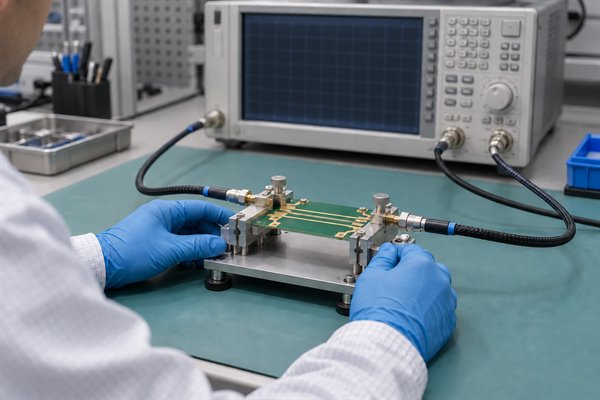
- TDR and impedance coupons: define coupon ownership, representative layers and structures, calibration, sampling, reported values, and failure disposition.
- Insertion loss, return loss, or S-parameters: request these only when the RF response is a purchase requirement, and define the test vehicle, ports, sweep, fixture, de-embedding, data format, and limits.
- Microsection: use it to check plating, dielectric, copper, lamination, and via or backdrill features selected in the inspection plan.
- Dimensional and X-ray inspection: apply these to registered layers, cavities, drilled features, hidden structures, or other RF-critical dimensions that cannot be confirmed visually.
- Bare-board electrical test: require continuity and isolation testing, while recognizing that it does not prove impedance, insertion loss, return loss, or complete RF performance.
- Material traceability: request laminate identity, lot or batch records, approved substitutes, and any storage or handling evidence required by the quality plan.
Standard bare-board electrical testing does not verify the complete RF performance of a high frequency PCB. The final plan should link each required test to a stated risk or acceptance criterion and identify whether it applies to first article, each lot, a sample, or periodic requalification.
What Files Should You Send for an Accurate High Frequency PCB Quote?
Send one revision-controlled package so every supplier prices the same board. Missing stackup, material, impedance, or test information forces each bidder to make different assumptions, which makes the returned prices impossible to compare fairly.
- Fabrication data: Gerber or ODB++, NC drill and route files, netlist if available, and a fabrication drawing with revision identity.
- Stackup: layer order, dielectric and copper targets, total thickness, controlled layers, reference planes, and allowed construction changes.
- Material callouts: exact laminate and bonding materials, thicknesses, copper type, electrical-data source, and approved alternates.
- Impedance and RF requirements: target table, tolerances, RF-sensitive geometry, operating band, loss or phase limits, and critical transitions.
- Mechanical and finish requirements: outline, tolerances, cavities, backdrill, metal backing, connector interfaces, solder mask, legend, and surface finish.
- Verification package: coupon, inspection, sampling, raw-data, report, certificate, traceability, and first-article requirements.
- Commercial inputs: prototype and production quantities, panel constraints, delivery destination, requested ship or arrival date, Incoterm, and packaging needs.
Identify unresolved items in the package rather than leaving them blank. Suppliers can then return the same open questions and quote assumptions, giving procurement a usable basis for comparison.
What Should a Useful DFM Review Tell You Before Production?
A useful RF DFM review should return the proposed build, every requested deviation, and the questions that still block release. A generic “files are manufacturable” reply does not show whether the supplier reviewed the RF-sensitive parts of the design.
- Proposed stackup: material set, dielectric targets, copper assumptions, pressed thickness, reference planes, and the geometry used for impedance calculation.
- Material status: availability, procurement time, minimum buy, shelf-life or storage concern, and any requested substitute.
- RF geometry changes: proposed trace, gap, ground clearance, mask, via, pad, launch, or coupon changes and their reason.
- Process limits: combinations of etching, registration, drilling, backdrill, filling, plating, cavity, metal backing, or panelization that need adjustment.
- Test approach: coupon design, correlation to production layers, sampling, method, fixtures, data format, acceptance limits, and unavailable measurements.
- Release questions: a short list of unresolved material, stackup, geometry, testing, documentation, or delivery decisions assigned to the responsible party.
Any proposed change that may alter RF performance should return to the customer for approval before production release. The approved DFM response then becomes part of the baseline used to review first article and repeat orders.
How Should You Compare RFQ Responses from Different Suppliers?
Compare the complete technical and delivery scope, not the unit price in isolation. For high frequency PCB in Switzerland, two offers are not equivalent if they use different laminates, stackups, test plans, manufacturing sites, or responsibility boundaries.
| RFQ Item | What Buyers Should Compare |
|---|---|
| Material | Exact laminate, bondply or prepreg, thickness, copper type, availability, and approved substitutes |
| Stackup | Returned construction, finished dielectric and copper targets, RF layers, reference planes, and deviations |
| Impedance | Targets, tolerances, calculation assumptions, coupon design, sampling, and reported data |
| RF testing | Included measurements, test structures, fixtures, frequency range, de-embedding, limits, and report format |
| Manufacturing site | Legal entity, actual plant, subcontracted operations, inspection location, and ship-from country |
| NRE | Tooling, CAM or engineering, coupons, test setup, reports, and repeat-order charges |
| Lead time | Material procurement, approval start point, fabrication, testing, shipment, customs, and partial-delivery terms |
| Change control | Material, construction, process, site, and test changes that require written customer approval |
Normalize the offers by listing every exclusion and assumption beside the quoted price. If one price omits the specified material, representative coupon, RF measurement, or approved build site, correct the scope before selecting a supplier.
If your project allows manufacture outside Switzerland, EBest Circuit can review the current design and return a proposed stackup, material options, DFM questions, and quotation. Ready to request a quote? Send your Gerber or ODB++ files, stackup, material callouts, impedance and RF requirements, quantities, test scope, and delivery destination to sales@bestpcbs.com.
FAQs About High Frequency PCB in Switzerland
Q1: Does a high frequency PCB for a Swiss project need to be manufactured in Switzerland?
A1: No, unless the contract, customer approval, data restriction, or qualification plan requires Swiss manufacture. If overseas or European production is allowed, name the approved plant and assign importing, customs, delivery, and return responsibilities before the order.
Q2: Is Rogers material always required for a high frequency PCB?
A2: No; Rogers is one group of RF laminate products, not a universal requirement. Select the material from the operating frequency, loss budget, impedance stability, thermal and mechanical needs, assembly process, supply status, and qualified electrical data.
Q3: Can PTFE and FR-4 be used in the same multilayer PCB?
A3: Yes, a qualified fabricator can build mixed PTFE/FR-4 constructions. The returned stackup must address bonding, thermal expansion, registration, resin flow, drilling, plating, finished thickness, and the RF geometry affected by the hybrid build.
Q4: Does TDR testing prove complete RF performance?
A4: No; TDR is primarily used to evaluate characteristic impedance and discontinuities. Loss, return loss, phase, launch behavior, resonance, and antenna performance may need separate test structures or system-level verification.
Q5: Can an RF PCB supplier substitute the specified laminate?
A5: Only when the RFQ permits substitution and the customer approves the proposed alternative. Compare Dk and Df under relevant methods and frequencies as well as thickness, copper, thermal, mechanical, processing, availability, and qualification effects.
Q6: Why can RF laminate availability affect lead time?
A6: Specialized cores, bondplies, thicknesses, or copper types may not be held in the required quantity. Procurement, minimum buys, lot allocation, incoming inspection, and shelf-life controls can add time before fabrication begins.
Q7: Should prototype and production boards use the same stackup?
A7: Use the production-intent stackup when prototype results will support qualification. If an early prototype uses a different material or construction, document the difference and repeat the affected electrical and reliability checks after transfer.
Q8: Can high frequency PCBs be manufactured in China and shipped to Switzerland?
A8: Yes, if the project permits Chinese manufacture and the supplier can meet the technical and documentation requirements. The buyer should define the approved factory, Incoterm, importer, customs data, VAT and clearance responsibility, packaging, delivery point, and nonconformance return route.
Q9: Does every high frequency PCB require S-parameter testing?
A9: No; the need depends on the controlled RF response and the product risk. Specify S-parameter testing when insertion loss, return loss, coupling, or another network response must be verified beyond impedance and ordinary electrical test.
Q10: What changes should trigger customer approval on repeat orders?
A10: Require approval for changes that can move the validated RF baseline. Typical triggers include laminate or bondply, dielectric or copper, impedance geometry, finish, drilling or backdrill, test method, coupon, subcontracted process, and manufacturing site.