PCB manufacturing PCB manufacturing
Home > Blog

microwave pcb design

Radio Frequency Circuit Board: Materials, Design Rules, and Cost Factors
Thursday, July 9th, 2026

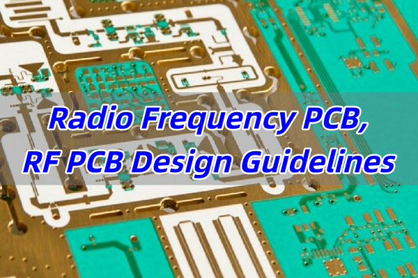
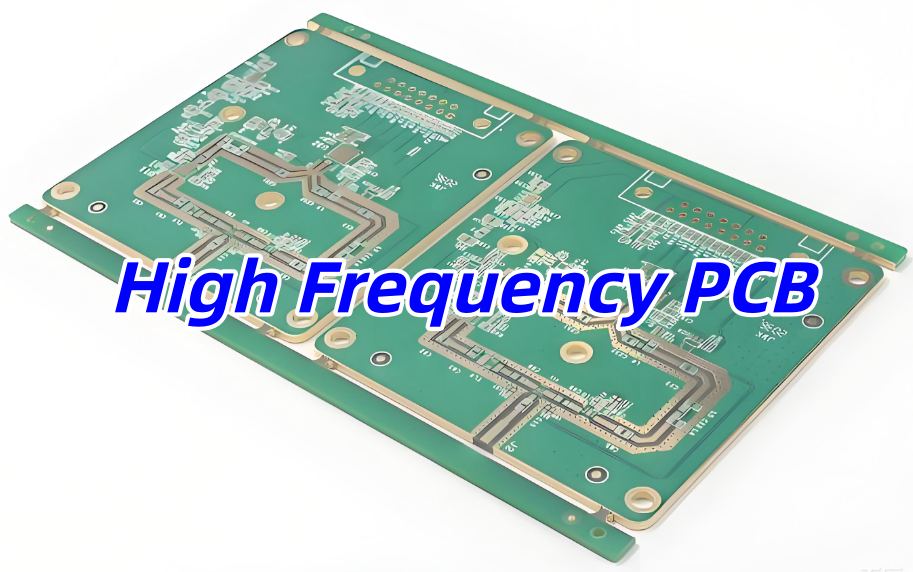
A radio frequency circuit board is a PCB designed to carry signals that are sensitive to impedance, loss, coupling, and electromagnetic behavior. In practical terms, that usually means the board layout, material choice, stackup, grounding, and connector transitions matter far more than they do on an ordinary low-speed control board.

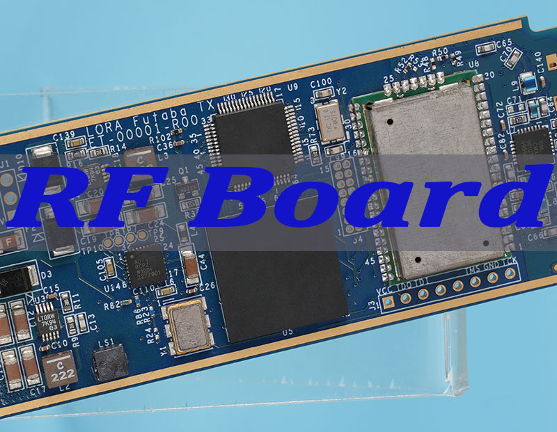
Not every board that includes a wireless module called RF PCB. The term usually applies when the board itself must support controlled high-frequency signal behavior, such as RF transmission lines, matching networks, filters, antennas, mixers, LNAs, PAs, or microwave interconnects. Once the frequency rises, the board is no longer just a mechanical carrier. It becomes part of the circuit.
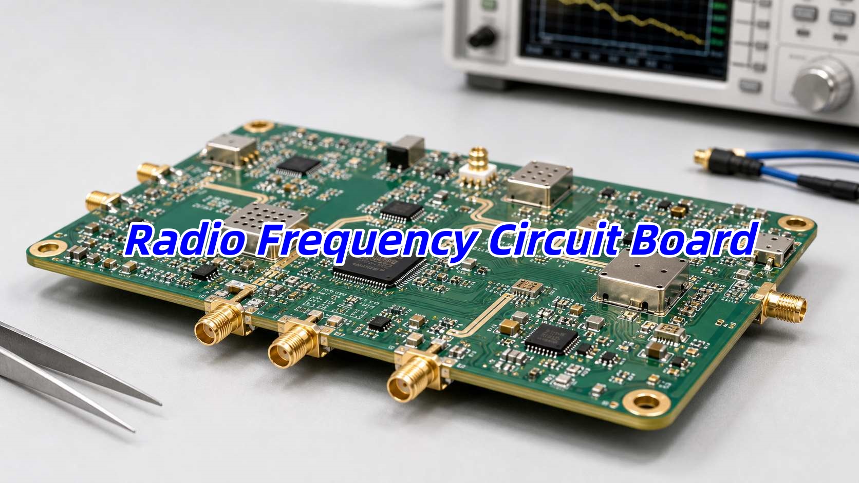
Radio Frequency Circuit Board

What Is a Radio Frequency Circuit Board?

A radio frequency circuit board, often called an RF PCB or high-frequency PCB, is a printed circuit board built for circuits that operate in the radio or microwave range. These boards are commonly used in wireless communication, radar, GPS, satellite systems, RF test equipment, automotive telematics, industrial sensing, medical devices, and IoT products.

The key difference from a standard FR-4 board is not just frequency. It is electrical predictability. An RF design needs controlled impedance, stable dielectric behavior, low insertion loss, good return paths, and a layout that limits radiation and coupling.

That is why the same schematic can behave very differently depending on the PCB material, copper geometry, via structure, and connector launch design.

When Is a Standard PCB Not Enough for RF Applications?

Many projects start on standard FR-4 because it is familiar and cost-effective. In some RF products, that is still the right choice. But once signal integrity, loss, or repeatability become tight, ordinary stackups may not be enough.

In general, a standard PCB becomes less suitable when the project includes:

  • Controlled RF transmission lines
  • High-frequency amplifiers or filters
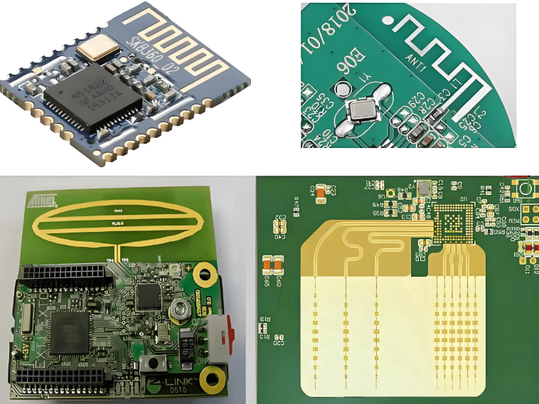
  • Antennas integrated on the board
  • Low-loss signal paths over meaningful distance
  • Tight phase or impedance consistency
  • Microwave connectors and launch structures
  • Multi-band or high-gain RF front ends

If a design only carries short RF traces between a certified module and an antenna connector, FR-4 may still be acceptable. If the board itself contains tuned RF structures, matching sections, or long controlled signal paths, material selection becomes much more critical.
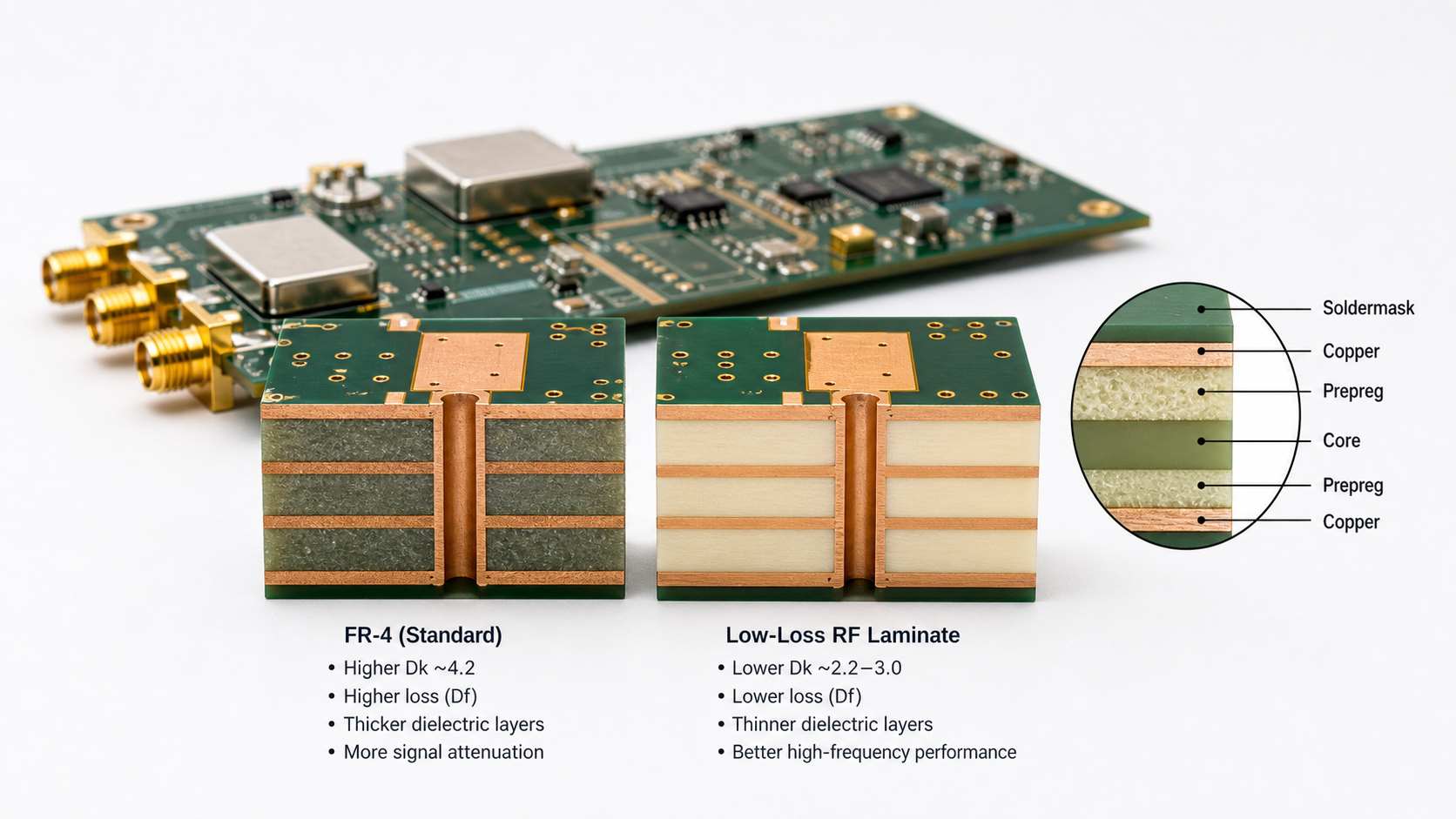
When Is a Standard PCB Not Enough for RF Applications?

Common Materials Used for RF Circuit Boards

The material decision is usually driven by dielectric constant stability, dissipation factor, temperature behavior, moisture absorption, and manufacturability.

Material TypeTypical UseMain AdvantageMain Trade-Off
Standard FR-4Lower-cost RF modules, mixed digital/RF boards, short RF tracesLow cost and easy fabricationHigher loss and less stable dielectric behavior
High-speed FR-4 / low-loss epoxyMid-range RF and mixed-signal boardsBetter loss performance than standard FR-4Still not ideal for demanding microwave designs
PTFE-based laminatesMicrowave, radar, satellite, low-loss RF pathsVery low loss and stable RF behaviorHigher material cost and more demanding processing
Hydrocarbon ceramic laminatesRF and microwave products needing a balance of cost and performanceBetter dimensional and RF stabilityMore expensive than ordinary FR-4
Hybrid stackupsMixed RF and digital boardsLets engineers control cost by using RF material only where neededLamination and DFM complexity increase

For many buyers, the important point is this: the best RF material is not always the most expensive one. It is the one that meets loss, impedance, and stability targets without adding unnecessary fabrication difficulty.

How Material Properties Affect RF PCB Performance?

At RF frequencies, the substrate is an electrical design variable, not just a base material.

The most important properties are:

  • Dielectric constant (Dk): affects trace width, signal velocity, and impedance control
  • Dissipation factor (Df): affects dielectric loss and insertion loss
  • Thickness tolerance: affects impedance repeatability
  • Copper surface profile: affects conductor loss at higher frequencies
  • Thermal stability: matters for power amplifiers and outdoor products
  • Moisture absorption: matters for frequency stability and reliability in harsh environments

If the dielectric constant shifts too much across frequency or production lots, the board can move off target even when the fabrication dimensions look correct.

RF PCB Stackup and Impedance Control

A radio frequency circuit board should be designed with the stackup settled early, not after routing is nearly done.

That is because the stackup controls:

  • Microstrip or stripline impedance
  • Reference plane continuity
  • Return current path quality
  • Trace spacing and coupling
  • Connector launch geometry
  • Via transition behavior

Most RF boards rely on microstrip or grounded coplanar waveguide structures on outer layers, because they are easier to tune and measure. Stripline can work well too, especially where shielding and coupling control matter more than easy tuning access.

Key Layout Rules for a Radio Frequency Circuit Board

At RF, a board can fail even when the schematic is correct. Layout decisions directly affect gain, noise, return loss, spurious response, and EMC behavior.

The most important layout rules usually include:

  • Keep RF traces short and direct
  • Avoid unnecessary layer transitions
  • Maintain continuous reference planes
  • Control trace width and spacing from the beginning
  • Isolate noisy digital, clock, and power-switching areas from sensitive RF paths
  • Place matching components close to the device pins they tune
  • Keep the ground via fence strategy consistent around critical RF regions
  • Minimize stubs at connectors, pads, and test access points

For higher-frequency boards, even pad shape, solder mask opening, and connector footprint transitions can noticeably change performance.

Why Grounding Matters More in RF PCB Design?

Grounding problems are one of the most common reasons RF boards behave differently in prototype, validation, and mass production.

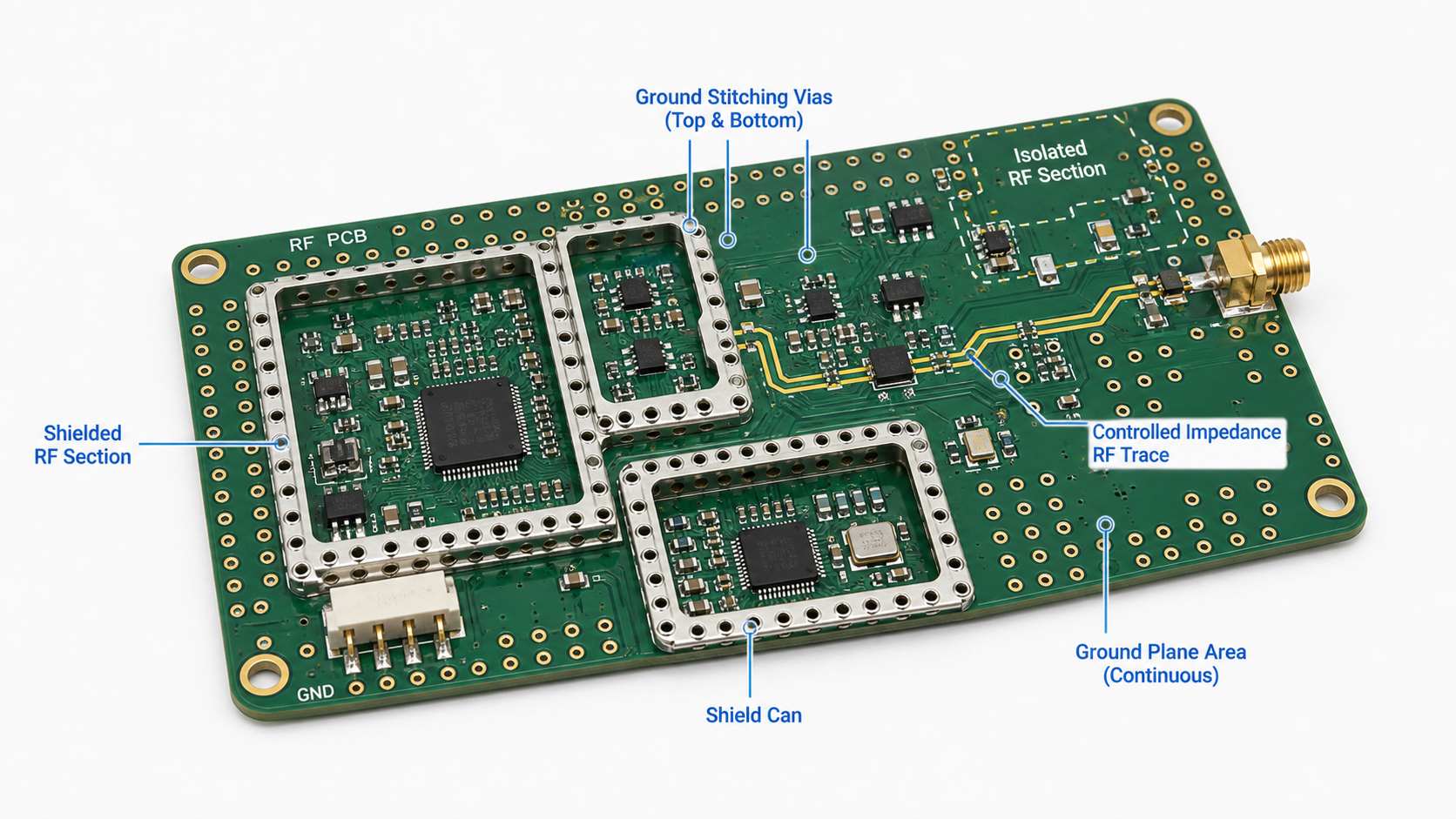
A good RF ground system is not just ā€œmore copper.ā€ It requires a predictable return path. Gaps in reference planes, poor stitching around transmission lines, and mixed return currents from digital and RF sections can all degrade performance.

In practical RF layouts, engineers often use:

  • Solid reference planes under RF traces
  • Stitching vias around RF boundaries and connector launches
  • Controlled grounding around antennas and shield cans
  • Partitioning between RF, analog, digital, and power sections

If the grounding strategy is weak, the board may show unstable tuning, increased loss, or unexpected radiation.
Why Grounding Matters More in RF PCB Design?

Vias, Connectors, and Transitions in High-Frequency Boards

At lower frequencies, vias and connectors are mostly interconnect details. At RF, they are part of the transmission path.

The decision logic is simple: every transition adds discontinuity, so transitions should be limited and designed intentionally.

RF Transition ElementMain ConcernPractical Design Focus
Signal viaInductance and impedance discontinuityReduce unnecessary transitions and optimize return path vias
Connector launchReflection and mismatchTune pad shape, anti-pad, and ground stitch pattern
Test point or stubAdded discontinuity and radiationAvoid on critical RF traces when possible
SMA or edge connector areaMechanical fit and RF continuityKeep launch geometry consistent with stackup
Board-to-board RF pathCoupling and lossShort path, controlled impedance, stable connector system

If the project includes microwave connectors, the launch region should usually be reviewed as a separate RF structure, not treated as a standard footprint.

Can FR-4 Be Used for a Radio Frequency Circuit Board?

Yes, but only within the right application boundary.

FR-4 can still be acceptable when:

  • RF frequency is modest
  • RF path is short
  • Insertion loss is not extremely tight
  • The design uses a certified RF module and the host board only carries short matched traces
  • Cost sensitivity is higher than peak RF performance

FR-4 becomes less attractive when:

  • Design includes long RF paths
  • Can be operates at higher microwave frequencies
  • phase consistency matters
  • Includes integrated antennas or distributed RF structures
  • Needs low loss and repeatable tuning across production lots

In other words, FR-4 is not ā€œwrong.ā€ It is just not universal.

Typical Applications of RF Circuit Boards

A radio frequency circuit board can appear in many industries, but the design priorities are not always the same.

Common applications include:

  • Wireless communication equipment
  • GPS and GNSS devices
  • Wi-Fi, Bluetooth, and IoT hardware
  • RF power amplifiers and front-end modules
  • Radar and sensing systems
  • Medical telemetry devices
  • Automotive RF electronics
  • Satellite and aerospace communication hardware
  • RF test and measurement equipment

For example, an IoT gateway may care most about mixed-signal integration and manufacturability, while a radar board may care more about loss, phase stability, and controlled transitions.

Manufacturing Challenges of RF PCBs

RF boards are often harder to manufacture consistently than standard digital boards because electrical behavior is tied closely to fabrication details.

The most common manufacturing challenges include:

  • Tighter impedance tolerance requirements
  • Laminate handling differences for PTFE-based materials
  • Dimensional stability during lamination
  • Copper roughness effects at higher frequency
  • Drill quality and registration around controlled transitions
  • Hybrid stackup bonding complexity
  • Solder mask influence near RF launch areas

That is why DFM review matters early. A board that works in simulation but ignores real fabrication tolerances can become expensive to debug later.

This is also where EBest Circuit (Best Technology) can be useful. For RF-related PCB or PCBA projects, the practical value is not just fabrication capacity. It is the ability to review stackup, manufacturability, material choice, and assembly fit before the project enters production.

RF PCB Assembly and Testing Considerations

RF assembly is not just ordinary SMT with different parts. Placement accuracy, connector alignment, shielding, cleaning control, and test setup can all affect final performance.

Important assembly and test concerns include:

  • Connector coplanarity and solder quality
  • Shield can placement and rework access
  • Stability of matching network components
  • Board cleanliness, especially where leakage or detuning matters
  • Cable and fixture repeatability during validation
  • Test method selection such as VNA measurement, insertion loss, return loss, or gain verification

For RF PCBA projects, buyers should also think ahead about whether they need bare-board delivery, assembly only, tuned prototype support, or functional RF test support.

What to Provide When Requesting a Quote for an RF Circuit Board

A useful RF quotation needs more than ā€œboard size and layer count.ā€

The most helpful files and notes usually include:

  • Gerber or ODB++ files
  • Layer stackup
  • Target impedance and trace type
  • Material preference or acceptable alternatives
  • Operating frequency range
  • Copper thickness
  • Connector type and launch details
  • Assembly requirement if PCBA is needed
  • RF test requirement if applicable
  • Prototype quantity and production forecast

If the board includes a special RF laminate, hybrid stackup, controlled launch area, or microwave connector, that should be stated clearly in the inquiry. Otherwise, the supplier may quote the board as if it were a standard PCB, which creates avoidable back-and-forth later.

How to Choose the Right RF PCB Manufacturer?

The right RF PCB supplier is not simply the one with the lowest laminate price. The better question is whether the supplier can support the actual engineering risk of the design.

A good evaluation checklist includes:

  • Experience with RF and high-frequency materials
  • Ability to support hybrid stackups if needed
  • Impedance control capability
  • Understanding of connector launch and grounding details
  • Assembly support for RF components and shielding
  • Test and inspection capability aligned with the product
  • Willingness to review DFM issues before build

For engineers moving from prototype into production, EBest Circuit’s one-stop PCB manufacturing, component sourcing, PCBA assembly, and technical review model can reduce handoff mistakes, especially when the design mixes RF, digital control, and power sections on one board.

Conclusion

A radio frequency circuit board is not just a normal PCB running at a higher speed. It is a board whose electrical behavior depends strongly on material properties, stackup structure, grounding, trace geometry, and transitions. The right material and layout choices depend on the actual RF function, not just the frequency number alone.

If you are evaluating an RF PCB or RF PCBA project, the most practical approach is to define the frequency range, loss target, impedance structure, material options, and assembly requirements early. For RF PCB and PCBA support, contact EBest Circuit at sales@bestpcbs.com.
You may also like

Top 10 RF Microwave PCB Manufacturers for High-Power Applications
Thursday, December 4th, 2025

High-power RF and microwave systems—such as RF amplifiers, 5G base stations, radar modules, satellite communication units, and microwave transmitters—require PCBs that can maintain stable performance under intense thermal and electrical stress. Ordinary FR-4 boards simply cannot handle the dielectric loss, heat generation, tight impedance requirements, and frequency-dependent behavior seen above 1 GHz.

In this guide, we highlight the Top 10 RF microwave PCB manufacturers for high-power applications—ideal for RF amplifiers, radar systems, 5G infrastructure, satellite communication, and other high-frequency uses.

Top 10 RF Microwave PCB Manufacturers for High-Power Applications

Why You Need a Specialized RF Microwave PCB Manufacturer?

High-power RF designs introduce challenges such as elevated heat, strict impedance requirements, and performance losses at microwave frequencies. Manufacturers must have:

  • Expertise in low-loss materials like Rogers, Taconic, or PTFE-based substrates
  • Multi-layer RF/microwave stackup engineering
  • High-precision etching and drilling for mmWave designs
  • Support for heat-sink integration, metal-backed PCBs, or thick-copper construction
  • Robust quality systems for aerospace/defense-grade reliability

Choosing the right vendor ensures stable power handling, lower insertion loss, and consistent performance across your operating frequency range.

Top 10 RF Microwave PCB Manufacturers for High-Power Applications

1. American Standard Circuits (ASC)

ASC is one of the most experienced RF microwave PCB manufacturers in North America. They specialize in complex high-power designs, including:

  • Metal-backed PCBs for heat dissipation
  • PTFE-based microwave laminates (Rogers, Taconic, Isola)
  • Tight impedance control
  • High-layer-count microwave PCBs

Best for: High-power RF, metal-backed microwave PCBs, aerospace/defense

Their engineering support for thermal-management and high-frequency performance makes them ideal for RF amplifiers and transmitters.

Top 10 RF Microwave PCB Manufacturers for High-Power Applications

2. HT Global Circuits

HT Global produces RF microwave PCBs operating up to 77 GHz and beyond. Their strengths include:

  • Multi-layer PTFE stackups
  • 2–20 layer RF/microwave builds
  • Heavy copper up to 6 oz for high-power devices
  • Hybrid stackups combining FR-4 with RF materials

They are a top choice for automotive radar, mmWave modules, and high-power RF designs.

Best for: mmWave, radar, low-loss PTFE boards, thick-copper RF PCBs

3. Summit Interconnect

Summit Interconnect is known for premium high-frequency and high-reliability microwave PCBs used in:

  • Aerospace
  • Defense
  • Telecom infrastructure

Their fabrication process emphasizes precision drilling, micro-vias, and controlled dielectric thickness—critical for high-frequency energy transfer and low insertion loss.

Best for: Mission-critical high-frequency systems

4. KKPCB

KKPCB works extensively with RF laminates such as Rogers, Isola, Taconic, and Panasonic materials. Their capabilities include:

  • Rigid, flex, and rigid-flex RF PCBs
  • Controlled impedance routing
  • Low-loss dielectric materials
  • High-density microwave layouts

A good mid-cost option for commercial RF/microwave products and 5G devices.

Best for: Telecom, 5G, RF modules

5. Highleap Electronics

Highleap supports complex microwave PCB builds requiring:

  • Hybrid materials
  • Multi-layer RF stackups
  • Cavity/RF shielding structures
  • Precise copper-weight control

Ideal for radar, satellite systems, and advanced RF sensing.

Best for: Multi-layer high-frequency and mmWave PCBs

6. RayMing Technology (RayPCB)

RayMing is widely referenced as a top microwave PCB manufacturer. Their key strengths include:

  • PTFE + hybrid dielectric combinations
  • High-frequency up to mmWave
  • ENIG, ENEPIG finishes for RF connectors
  • HDI for mixed digital + RF sections

Great for high-frequency testing equipment, RF sensors, and wireless communication modules.

Best for: Broad RF material selection, advanced stackups

7. WellPCB

WellPCB provides high-frequency PCBs up to 64 layers with:

  • Tight impedance tolerances
  • Low-loss laminates (Rogers, Isola, Taconic)
  • Quick-turn RF prototyping capability

A strong choice for R&D labs, engineering teams, and rapid iteration cycles.

Best for: Low-loss microwave PCBs and prototype runs

8. Sanmina Corporation

Sanmina serves enterprise and industrial markets requiring:

  • High-reliability RF PCB mass production
  • Telecom and infrastructure RF boards
  • Integrated assembly + testing

If your product needs scale, Sanmina is a top-tier partner.

Best for: High-volume microwave PCB production

9. TTM Technologies

TTM is one of the world’s largest PCB manufacturers with deep expertise in:

  • Microwave PCBs for defense/avionics
  • Very tight tolerance stackups
  • Hybrid laminates for both RF + digital

Perfect for mission-critical high-power RF systems.

Best for: High-reliability aerospace/defense RF PCBs

10. EBest Circuit (Best Technology) (BEST TECH)

EBest Circuit (Best Technology) stands out for its deep expertise in Rogers, Taconic, PTFE, ceramic-filled laminates, and hybrid RF stackups. Our core strengths include:

  • High-power RF PCB manufacturing with thick copper
  • PTFE microwave PCBs for >10 GHz
  • Cavity structures, tight impedance control, and controlled Dk/Df
  • RF prototype-to-production support

We are especially strong in thermal management, cost-effective PTFE processing, and mixed-material high-frequency boards used in RF amplifiers and microwave modules.

Best for: Custom high-power RF PCB manufacturing & PTFE-based microwave PCBs

What Should You Provide for High-Power RF PCBs?

When ordering high-power RF microwave PCBs, your manufacturer needs precise engineering data to ensure correct impedance, dielectric performance, and thermal stability. Below is a complete checklist.

1. Operating Frequency Range

Specify the exact frequency band, such as:

  • 1–6 GHz (RF)
  • 10–30 GHz (Microwave)
  • 24–77 GHz (mmWave)

Higher frequencies require lower-loss materials and tighter tolerances.

2. Target Impedance & Tolerance

Provide the intended impedance values such as:

  • 50Ī© microstrip
  • 75Ī© signal lines
  • Differential RF pairs

This allows the PCB manufacturer to determine trace width, spacing, copper thickness, and dielectric thickness.

3. Expected Power Handling / Heat Load

Thermal load affects stackup and material choice, especially for:

  • RF amplifiers
  • High-power transmitters
  • Power combiners/splitters

Manufacturers may include metal-backed substrates or copper coins if required.

4. Material Preferences

List materials if known:

  • Rogers 4350B, 4003C, 5880, 3006
  • Taconic TLX, TLY, RF-35
  • Isola Astra / I-Tera HT / PTFE laminates

Or request material recommendations based on your frequency and power.

5. Stackup Requirements

Specify:

  • Number of layers
  • Hybrid stackup (PTFE + FR-4)
  • Dielectric thickness
  • Copper weight (e.g., 1oz, 2oz, 3oz+)

High-power RF typically needs high-copper layers for heat dissipation.

6. RF-sensitive Structure Information

Provide details on:

  • RF cavities
  • Via fences / Ground vias
  • Via-in-pad for RF chips
  • Microstrip or stripline routing

These influence manufacturability and RF performance.

7. Connector Type & Finish

RF connectors need stable surface performance:

  • ENIG
  • ENEPIG
  • Hard gold

Let the manufacturer know if you’re using SMA, MMCX, SMP, or edge-launch connectors. Please remember, the more detailed information you provided, the fast you get your prototype.

What Should You Provide for High-Power RF PCBs?

What Should You Provide for High-Power RF PCBs?

Why EBest Circuit (Best Technology) Is Your Best Partner?

EBest Circuit (Best Technology) is one of the most leading radio frequency manufacturers in Asia, we have more than 19 years experienced in this field. Our team deeply specializing in high-power RF PCBs and PTFE-based microwave PCB fabrication. Here’s why we stand out for most years:

1. Expertise in High-Frequency Materials

BEST TECH processes complex RF materials including:

  • Rogers (4350B, 5880, 3003)
  • Taconic
  • Teflon/PTFE
  • Ceramic-filled laminates

2. Superior High-Power Handling Capability

Their thick-copper RF PCB options (2–6 oz) ensure stable thermal performance in:

  • Power amplifiers (PA)
  • High-power transmitters
  • RF power distribution networks

3. Precision Fabrication & Tight Impedance Control

With advanced drilling, lamination, and copper etching technologies, they achieve:

  • ±5% impedance tolerance
  • Excellent line width stability
  • Accurate dielectric thickness across the panel

4. RF Prototyping + Mass Production

From engineering samples to volume production, EBest Circuit (Best Technology) supports fast lead times with stable process control.

5. Competitive Pricing for PTFE & Microwave Boards

Compared with Western manufacturers, BEST TECH offers better pricing while maintaining high quality—ideal for startups, R&D teams, and cost-sensitive RF applications.

If you are interested in RF PCB design or want to get your first RF PCB prototype with fast delivery, please do not hesitate to contact us, our sales team are engineered sales, they deeply know the RF PCB, and enable to provide you the best solution and competitive price in short time.

FAQs

1. What is an RF microwave PCB?

An RF microwave PCB is a printed circuit board designed to operate at high frequencies (1–100+ GHz). It uses low-loss materials such as Rogers or PTFE to maintain stable impedance and minimize signal attenuation.

2. What causes high-power RF PCBs to fail?

Common failure causes include:

  • Excessive heat
  • Poor thermal design
  • Incorrect stackup selection
  • Impedance mismatch
  • Delamination from improper lamination of PTFE materials

Choosing the right RF PCB manufacturer greatly reduces failure risk.

3. What is the recommended copper thickness for high-power microwave PCBs?

For heat-heavy RF circuits:

  • 2 oz or 3 oz copper is common
  • 4–6 oz for very high-power amplifiers

4. Why is controlled impedance so important in RF PCB design?

Proper impedance ensures:

  • Lower insertion loss
  • Minimal signal reflection
  • Stable RF phase and amplitude
  • Accurate high-frequency performance

5. Can I use FR-4 for microwave PCBs?

FR-4 is not recommended above 3–6 GHz due to high dielectric loss. For microwave frequencies, PTFE or Rogers materials are necessary.

You may also like

What is a Microwave PCB? An Ultimate Guide 2026
Wednesday, December 3rd, 2025

A microwave PCB handles signals that run at very high frequencies, and these boards support systems that need clean, stable performance. You will find a microwave PCB in equipment such as radar modules, satellite links, high-speed wireless platforms, and precision test devices. As industries push toward higher data rates and smaller RF systems, the need for dependable microwave boards grows quickly.

Today, many engineers search for rf microwave PCB options that keep loss low and impedance steady. Others look for complete rf & microwave PCB solutions that simplify material choice, stack-up planning, and manufacturing. If you’re evaluating RF microwave PCB materials or sourcing RF & microwave PCB solutions, this article will give you a complete understanding.

What is a Microwave PCB? An Ultimate Guide 2026

What Is a Microwave PCB?

A microwave PCB is a printed circuit board designed to operate at extremely high frequencies, typically:

  • Microwave band: 300 MHz – 30 GHz
  • Millimeter-wave (mmWave): 30 – 100+ GHz

At these frequencies, PCB traces behave like transmission lines, and even tiny layout variations can impact signal loss, phase accuracy, antenna performance, and overall system reliability.

Microwave PCBs are commonly used in radar systems, satellite communication, aerospace navigation, and 5G mmWave modules. Compared with standard RF boards, microwave PCBs demand more precise materials, controlled impedance, and stricter fabrication tolerances.

What Materials Are Used for Microwave PCBs?

Material choice is one of the most important decisions in microwave design. Standard FR-4 cannot support microwave frequencies due to high loss and unstable dielectric properties. Instead, microwave PCBs use advanced materials engineered for low loss and tight dielectric tolerances.

Here are the materials most commonly used:

Material TypeExamplesFeaturesBest Use Case
PTFE (Teflon)RT/duroid 5880, Taconic TLYExtremely low loss, stable Dk, best for high GHzRadar, mmWave, satellites
Hydrocarbon CeramicsRogers RO4350B, RO4003CLow loss, easy to manufacture, cost-effective1–20 GHz microwave circuits
Ceramic-Filled PTFERogers RO3006/3010Ultra-stable Dk, low thermal expansionHigh-power microwave and phased arrays
Hybrid StackupsFR4 + RogersPerformance + lower costMixed-signal RF/microwave designs

The best material depends on target frequency, environmental exposure, and mechanical requirements. Each laminate affects loss, phase stability, and long-term reliability.

Key Design Rules and Layout for Microwave PCB Design

Designing a microwave PCB is very different from routing a standard digital or low-frequency board. At microwave frequencies, each copper trace behaves like a transmission line. Small changes in width, dielectric height, copper roughness, or via structure can shift impedance and alter the entire RF chain. Because of that, layout and stack-up design must follow strict engineering rules to keep signal quality stable.

Key Design Rules and Layout for Microwave PCB Design

Below are the core principles used by RF engineers when building reliable microwave layouts.

1. Maintain Tight Impedance Control

Stable impedance is the foundation of microwave design. Even small dimensional changes can introduce reflections or distort the waveform.

Key requirements:

  • Define target impedance early (commonly 50Ī© or 75Ī©).
  • Choose the correct structure: microstrip, stripline, or grounded coplanar waveguide (GCPW).
  • Keep trace width consistent along the entire path.
  • Maintain stable dielectric thickness and copper thickness.
  • Use field-solver tools (ADS, HFSS, CST, Polar SI, or Altium impedance calculator).
  • Keep differential pairs phase-matched if used in RF mixers or high-frequency paths.

GCPW is widely used for microwave PCB design because it offers strong field confinement and supports compact layouts.

2. Use Smooth Routing Instead of Sharp Corners

High-frequency energy does not like sudden changes. Sharp corners cause impedance shifts and increase local reflections.

Preferred routing practices:

  • Avoid 90° turns.
  • Use gradual curves (arc routing) for cleaner field transitions.
  • Use mitered 45° bends if space is limited.
  • Keep sensitive paths straight and short whenever possible.

Smooth routing helps preserve phase stability and reduces insertion loss.

3. Keep the Ground Plane Continuous

A microwave signal needs a clean, uninterrupted return path. Gaps in the ground plane cause radiation, coupling, and impedance drift.

Ground plane guidelines:

  • Maintain a solid ground layer directly under RF traces.
  • Avoid splits, voids, or cutouts beneath the signal path.
  • Do not place digital return paths through RF areas.
  • Add stitching vias around RF traces to create a ā€œvia fenceā€ barrier.

A well-designed ground structure stabilizes the electromagnetic field and reduces unwanted emissions.

4. Manage Vias Carefully

A via is not just a hole at microwave frequencies—it’s a small inductor. Too much via inductance can degrade signal quality.

Best practices for vias:

  • Avoid unnecessary layer jumps.
  • Use multiple parallel vias to lower effective inductance.
  • Keep via barrels short when possible.
  • Add grounding vias around pads and connectors to improve shielding.
  • Avoid routing RF traces directly over via fields or ground voids.

Good via strategy can significantly improve stability in PA, LNA, and filter sections.

5. Select the Right Transmission Line Structure

Different RF paths require different structures depending on frequency, isolation, and mechanical constraints.

Common options:

  • Microstrip – simple, ideal for top-layer routing.
  • Stripline – fully shielded, good for noise-sensitive circuits.
  • Grounded coplanar waveguide (GCPW) – excellent isolation, compact layout, and easy impedance tuning.
  • Wide microstrip – lower conductor loss, suitable for power amplifiers.

GCPW has become the most popular for microwave work due to its predictable behavior and high routing density.

6. Align Components with the Signal Flow

Component orientation affects load matching and return loss.

Component placement guidelines:

  • Place RF blocks (filter, LNA, PA, mixer) in the order of the signal chain.
  • Keep matching networks close to device pins.
  • Avoid unnecessary gaps between RF parts.
  • Place RF connectors, such as SMA or SMP, near the board edge for clean transitions.

When Should You Choose Microwave PCB vs. RF PCB?

Many engineers compare microwave PCBs with standard RF boards because both handle high-frequency signals. But the decision depends on frequency, performance targets, and loss tolerance.

TechnologyFrequency RangeBest For
RF PCBUp to ~6 GHzBluetooth, Wi-Fi, sub-6 GHz communication
Microwave PCB6–100+ GHz5G mmWave, radar, satellite, high-precision sensing

Choose an RF PCB when:

  • Frequencies are below 6 GHz
  • Cost is a major concern
  • FR-4 or mixed-material stackups are acceptable

Choose a Microwave PCB when:

  • You operate above 6 GHz
  • You require ultra-low loss
  • Your system needs stable phase and predictable impedance
  • Applications involve radar, mmWave, or satellite links

In short, microwave PCBs suit high-precision projects where even small layout or material changes can affect real performance. They are the preferred choice for radar, satellite links, and advanced communications.

Microwave PCBs Applications & Industries

Microwave PCBs appear in many sectors because they support stable, low-loss transmission for sensitive circuits. You’ll often see them in systems that require fast data, long-range signal paths, or precise sensing.

Common applications include:

  • 5G and 6G wireless infrastructure
  • Satellite communication systems (SATCOM)
  • Automotive radar (24 GHz, 77 GHz)
  • Military and commercial radar platforms
  • Microwave filters, couplers, and antennas
  • High-frequency power amplifiers
  • Navigation and guidance systems
  • Medical imaging devices such as MRI coils
  • Instrumentation and RF test equipment
  • Industrial microwave heating and sensing

These industries rely on microwave boards because small performance shifts can affect overall system behavior. Stable materials and predictable routing keep these systems accurate and responsive.

Microwave PCBs Applications & Industries

Does Size of a Microwave PCB Affect Its Application?

Yes, board size can influence performance because microwave signals respond to physical dimensions. At these frequencies, even a few millimeters can change how energy travels.

Board size affects:

  • Impedance stability:Longer traces add more loss and potential phase distortion.
  • Resonance behavior:Larger boards can introduce unwanted resonances.
  • Shielding structure:Compact layouts may need tighter via fences.
  • Thermal changes:Bigger boards may expand more under heat, shifting dielectric spacing.
  • Antenna performance:Antenna length and board shape affect radiation patterns.

Small boards require sharper tolerance control. Large boards demand stronger handling of expansion and material stability. The ideal size depends on whether the circuit is an antenna, filter, amplifier, or sensor.

How to Tell If a Microwave Control Board Is Bad?

Many users ask this because microwave ovens and industrial microwave systems depend on small control boards. Failures are often easy to spot once you know what to check. Common signs of a bad microwave control board include:

  • No power, no response, or blank display
  • Buttons that fail to react
  • Burning smell or visible damage
  • Unusual noises or sparking
  • Microwave stops heating while lights and fan still work
  • Random behavior such as auto-starting or shutting off
  • Relays that click repeatedly without function

If above signs occur, you can perform below visual checks safely:

  • Scorch marks or dark spots
  • Swollen capacitors
  • Cracked solder joints
  • Damaged connectors
  • Loose ribbon cables

These symptoms point to circuitry or relay failure. For home microwaves, technicians often replace the entire board rather than repair individual components.

How Much Does It Cost to Repair a Microwave Circuit Board?

Repair cost depends on equipment type, part availability, and labor requirements.

Typical consumer microwave repair ranges:

  • Basic repair: USD 80–120
  • Control board replacement: USD 120–250
  • High-end or built-in models: USD 180–350

Industrial microwave equipment repair ranges:

  • Board-level component repair: USD 250–600
  • Full board replacement: USD 400–1,200+ depending on complexity

Factors that influence cost include:

  • Part scarcity
  • Board size and layer count
  • Number of relays, sensors, or high-voltage circuits
  • Whether the board is conformal-coated
  • Testing and calibration requirements

Consumer microwaves are often cheaper to replace than repair, but industrial microwave systems usually justify board-level repair. EBest Circuit (Best Technology) can repair the microwave circuit board for free if your PCB are ordered from our company.

Where to Get RF Microwave PCB Boards with UL/CE Certification?

Many companies need microwave PCBs that meet safety and compliance standards, especially when the final product enters global markets. UL and CE certifications help confirm material reliability and safety. When sourcing certified microwave boards, a good supplier should provide:

  • UL-certified laminates (Rogers, Taconic, Arlon, Panasonic)
  • CE-compliant production and testing
  • Rogers/PTFE/ceramic microwave PCB fabrication
  • Controlled impedance testing reports
  • Hybrid laminations and multi-layer microwave stackups
  • RF & microwave PCB solutions for 1–100 GHz

EBest Circuit (Best Technology) is a strong option for RF and microwave PCB production because the company offers:

  • UL-approved material systems
  • Stable performance with PTFE, Rogers, and ceramic-filled substrates
  • Tight impedance control for microwave designs
  • Complete CE-related documentation support
  • Strong engineering assistance during stack-up and DFM review
  • Consistent production with IPC standards
  • Fast global delivery for prototypes and batches

If you are preparing a new microwave PCB or RF hardware program, welcome to contact us at sales@bestpcbs.com, our team is 24/7 hours online for you!

You may also like