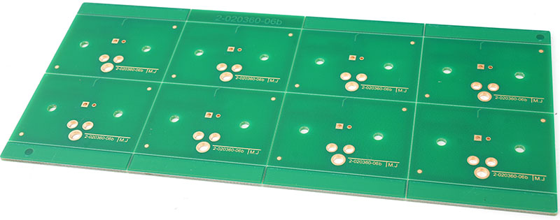
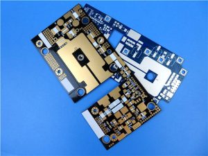
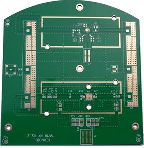
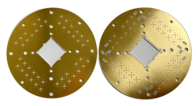
RF board, or Radio Frequency Printed Circuit Board, is engineered for circuits operating at high frequencies where signal integrity becomes highly sensitive to material properties. Typical RF designs work in the range of 300 MHz to 3 GHz, and many advanced systems extend far beyond this.
At these frequencies, standard FR4 materials often fail to maintain stable dielectric performance and low signal loss. As a result, specialized high frequency laminates are required. RF PCBs are therefore built using materials with low dielectric loss (Df) and stable dielectric constant (Dk) to ensure consistent signal transmission.
RF board is ideal for applications with higher operating frequency requirements. Right now, we normally use following material:
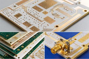
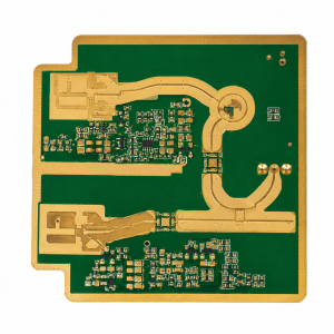
These boards are widely used in applications such as:
Wireless communication systems
RF antennas and modules
Automotive radar (ADAS)
Satellite and aerospace electronics
Microwave devices
IoT and high-speed signal systems
Why Use RF PCB Instead of Standard FR4?
FR4 is cost-effective and widely used, but its dielectric properties vary significantly at high frequencies. This leads to signal loss, impedance instability, and reduced system reliability in RF designs.
More stable dielectric constant across frequency range
Better impedance control
Reduced signal distortion
Improved phase consistency
What Materials Are Used in RF PCB?
Material selection is the core of RF PCB performance. Different applications require different dielectric properties and processing characteristics.
Common RF PCB Materials
1. Rogers Laminates
Widely used in RF and microwave circuits due to balanced performance and manufacturability.
Typical grades include:
RO4003C
RO4350B
RO4233
These materials offer:
Stable dielectric constant
Low loss tangent
Good thermal reliability
2. PTFE-Based Materials (Teflon)
Used in more demanding RF designs where ultra-low loss is critical.
Advantages:
Extremely low dielectric loss
Excellent high frequency performance
Considerations:
More complex processing
Higher manufacturing cost
Copper Thickness Range
Standard: 1/4 oz to 2 oz
Custom: based on current load and thermal design
Rogers is often the practical choice for most RF designs, while PTFE is used when performance requirements are more demanding.
Rogers Laminate Material Parameters
Choosing the right Rogers material directly affects signal integrity, impedance stability, and insertion loss. Below is a comparison of commonly used Rogers laminates for RF PCB applications.
Material
Dielectric Constant (Dk @10GHz)
Loss Tangent (Df @10GHz)
Thermal Conductivity (W/m·K)
Typical Application
RO4350B
3.48 ±0.05
0.0037
0.62
General RF, antennas, automotive radar
RO4003C
3.55 ±0.05
0.0027
0.71
RF communication, microwave circuits
RO4233
3.30 ±0.05
0.0025
0.65
High frequency, low loss applications
RT5880
2.20 ±0.02
0.0009
0.20
Ultra-low loss, aerospace, high-end RF
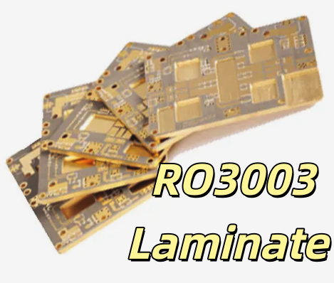
RO3003
3.00 ±0.04
0.0013
0.50
High stability circuits, precision RF
RO3010
10.2 ±0.25
0.0023
0.95
High dielectric designs, compact circuits
RF Board Capability
Base material: Rogers/Telfon
Board Thickness: 0.5mm~3.0mm(0.02″~0.12″)
Copper thickness: 0.5 OZ, 1.0 OZ, 2.0 OZ, 3.0 OZ
Outline: Routing, punching, V-Cut
Soldermask: White/Black/Blue/Green/Red Oil
Legend/Silkscreen Color: Black/White
Surface finishing: Immersion Gold, HASL, OSP
Max Panel size: 600*500mm(23.62″*19.68″)
Packing: Vacuum/Plastic bag
Samples L/T: 7~9 Days
MP L/T: 8~10 Days
RF PCB FAQs
1. What frequency requires RF PCB instead of FR4?
Typically, designs above 1 GHz or requiring strict impedance control should consider RF materials. Lower frequencies may still use FR4 depending on performance tolerance.
2. Is Rogers better than FR4?
For high frequency applications, yes. Rogers offers lower loss and more stable dielectric properties, which improves signal integrity.
3. Why is PTFE PCB more expensive?
PTFE materials are harder to process and require specialized manufacturing steps, which increases production cost.
4. Can RF PCB be used for mixed signal designs?
Yes. Hybrid stackups combining RF materials and FR4 are commonly used to balance performance and cost.
Start Your RF PCB Project Today
If you are designing RF or microwave circuits, choosing the right PCB is critical to performance.
At Best Technology, we combine material expertise, process control, and engineering support to deliver reliable RF PCB solutions.
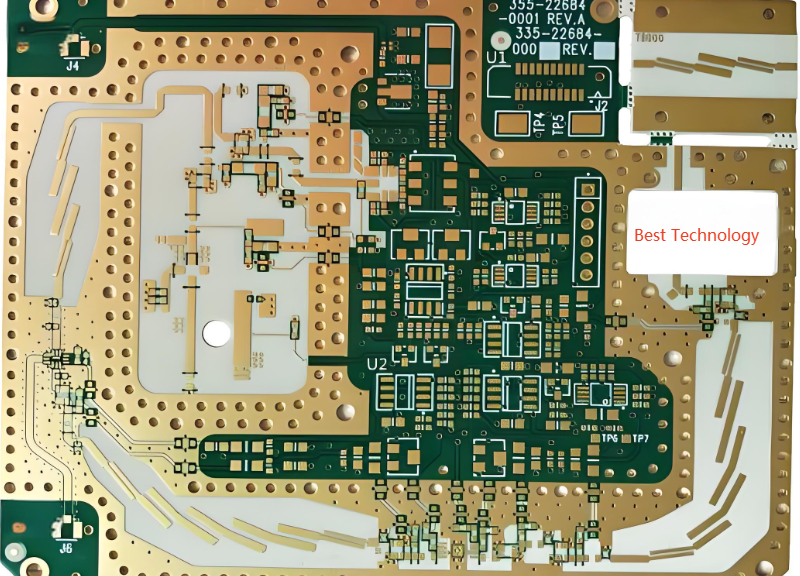
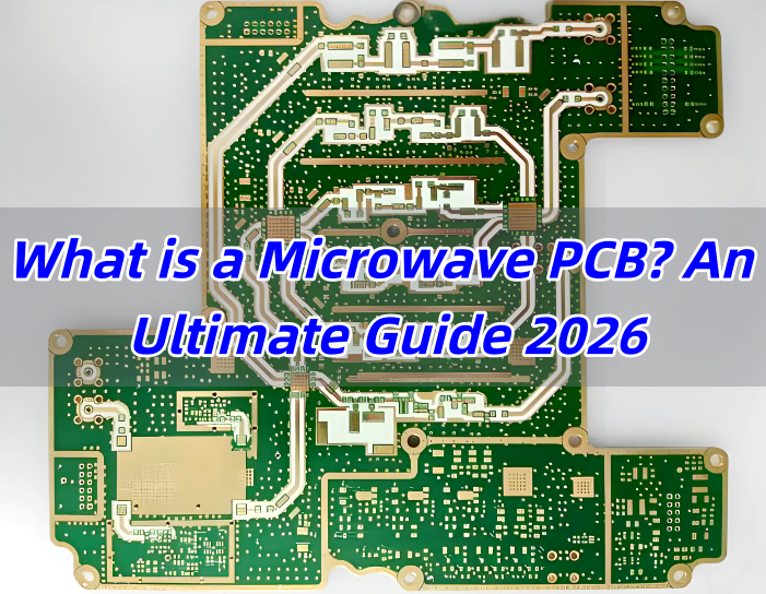
Radio frequency circuit board is a specialized printed circuit board designed to carry, process, and control high-frequency electromagnetic signals typically ranging from 100 MHz to 110 GHz. It forms the critical backbone of modern wireless and high-speed communication systems, enabling devices to transmit and receive signals with high precision and minimal loss across RF, microwave, and millimeter-wave bands.
Engineers and procurement managers often face significant hurdles when sourcing and developing high-frequency boards. Are you struggling to balance performance, cost, and speed in your RF development cycle?
Design Complexity: Small routing errors cause major high-frequency issues.
Signal Integrity: GHz signals need strict impedance and low-loss materials.
Manufacturing Gaps: Many factories lack true microwave-grade capability.
High Material Cost: Premium RF laminates increase BOM pressure.
Slow Cycles: Traditional prototype loops delay launches.
How a Specialized RF PCB Provider Delivers Solutions:
RF Design Support: Expert guidance for cleaner, correct layouts.
Better Materials: Rogers, Taconic, and proven RF options on hand.
Cost-Smart Selection: Materials matched to performance needs.
Quick-Turn PCBA: Fast PCB + assembly to speed development.
This comprehensive guide will explore the design, materials, manufacturing leaders, and best practices that define high-performance RF PCB technology, with a focus on achieving tailored solutions and rapid production. EBest Circuit (Best Technology) is a professional RF PCB manufacturer specializing in high-performance, low-loss boards for RF, microwave, and millimeter-wave applications. We hold ISO 13485medical certification and AS9100 aerospace certification, ensuring compliance with strict reliability and safety requirements.
Our PCB fabrication and SMT assembly lines are supported by a full MES system, providing complete production traceability and stable process control. Combined with expert RF design support and quick-turn PCBA services, we help customers achieve both high-frequency performance and fast development cycles. For your next RF board requirement, feel free to contact us at sales@bestpcbs.com.
What Is a Radio Frequency Circuit Board and How Does It Enable High-Frequency Performance?
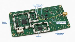
A Radio Frequency Circuit Board (RF PCB) is a specialized printed circuit board engineered to transmit, route, and manage high-frequency electromagnetic signals across the RF, microwave, and millimeter-wave spectrum, typically spanning 100 MHz to 110 GHz. At these frequencies, PCB materials, stack-ups, and routing rules must be optimized to preserve signal integrity, minimize loss, and maintain strict impedance control.
Core Enablers of High-Frequency Performance:
Controlled Impedance: Precise management of trace geometry and dielectric properties to maintain a consistent characteristic impedance (e.g., 50Ω), preventing signal reflections.
Low-Loss Materials: Use of specialized RF PCB materials with low dielectric loss (Df) and stable dielectric constant (Dk) across frequency and temperature, crucial for microwave PCBs.
Minimized Signal Path: Careful RF PCB routing to keep high-frequency traces short and direct, reducing attenuation and radiation.
Grounding & Shielding: Extensive use of ground planes and shielding techniques to contain electromagnetic fields and reduce crosstalk between the RF circuit and other board sections.
Quality of Conductors: Use of high-surface-quality copper with minimal roughness to reduce conductor loss at high frequencies.
In summary, an RF board is a carefully engineered system where every element—from laminate to layout—is optimized to guide high-frequency signals efficiently and predictably, forming the foundation of any reliable wireless device.
Why Do China Radio Frequency Circuit Board Suppliers Lead in Cost-Effective RF Manufacturing?
China-based suppliers have become dominant in the global RF PCB market by creating a powerful ecosystem that balances advanced technical capability with significant cost advantages. This leadership stems from a combination of scale, supply chain integration, and evolving expertise.
Key Drivers of Cost-Effectiveness:
Driver
Explanation
Integrated Supply Chain
Local sourcing of laminates, copper, and chemicals cuts logistics cost and shortens lead time.
Economies of Scale
High-volume RF production lowers per-unit pricing.
Skilled Engineering Talent
Mature RF design and manufacturing workforce ensures stable quality.
Advanced Manufacturing Equipment
LDI, AOI, and impedance-control systems support complex RF builds.
Government & Industry Support
Policies encourage investment, R&D, and continuous capability upgrades.
While cost is a primary factor, leading China radio frequency circuit board suppliers have moved beyond being just low-cost providers. They now compete on their ability to reliably produce complex, multi-layer radio frequency printed circuit boards with strict impedance control, making them a go-to for both cost-sensitive and performance-oriented projects.
How Do Radio Frequency Circuit Board Manufacturers Ensure Stability at High Frequencies?
Stability at high frequencies is non-negotiable for RF circuits. It ensures that a device performs consistently under varying operating conditions like temperature shifts, frequency changes, and over time. RF PCB manufacturers achieve this through meticulous control over materials, processes, and design for manufacturability (DFM).
Manufacturers ensure stability by focusing on several critical fronts:
Material Consistency: Using laminates with a stable Dielectric Constant (Dk) across temperature and frequency. Variations in Dk directly change impedance and signal velocity. Premium RF PCB materials from Rogers or Taconic offer superior stability over standard FR-4.
Precision Fabrication: Maintaining extremely tight tolerances on trace width, spacing, and dielectric thickness. A small deviation can alter the characteristic impedance, causing reflections and signal loss. This is paramount for microwave PCB performance.
Low-Loss Processing: Employing processes that minimize surface roughness of copper traces. At high frequencies, signal travel is confined to the conductor’s surface (skin effect). Rough surfaces increase the effective path length and resistance, leading to higher insertion loss.
Robust Lamination: Ensuring perfect bonding between layers without voids or delamination. Imperfections can create localized changes in the dielectric environment, harming performance.
Environmental Protection: Applying appropriate surface finishes (such as ENIG or immersion silver) that provide a solderable, flat surface and protect the copper from oxidation, which can degrade performance over time.
Through this multi-pronged approach, a reliable RF PCB manufacturer delivers boards that not only meet specifications on the test bench but also maintain their radio frequency circuit performance in the real world, ensuring the long-term reliability of the end product.
Top 10 Radio Frequency Circuit Board Manufacturers
Selecting the right manufacturer is crucial for the success of your RF PCB projects. The best partners combine technical expertise in high-frequency materials and processes with reliable execution. Here is a brief introduction to ten notable manufacturers in this space, including our own capabilities at EBest Circuit (Best Technology).
EBest Circuit (Best Technology): A specialized provider focused on quick-turn, high-mix, and prototype to mid-volume production. We excel in offering tailored RF PCB design support and rapid PCBA services, making us an ideal partner for fast-paced development cycles and specialized medical and IOT applications.
Würth Elektronik: A global leader offering high-quality PCB substrates (like their WE-series laminates) and full PCB manufacturing services, known for strong technical support and material science expertise.
Rogers Corporation: Primarily a material innovator, Rogers also offers advanced PCB fabrication services through their facilities, providing unparalleled expertise in processing their own high-performance laminates for extreme microwave PCBs.
TTM Technologies: A major volume manufacturer with extensive capabilities in advanced technologies, including RF/microwave PCBs for aerospace, defense, and high-end communications infrastructure.
Sierra Circuits: Well-known in the North American market for their proto-to-production services and strong emphasis on RF PCB design guidelines and educational resources, catering well to engineers.
Eurocircuits: A European-based manufacturer popular for prototyping and small-batch production, offering user-friendly platforms and consistent quality for various PCB types, including RF.
PCBWay / JLCPCB: These China-based giants dominate the online, low-cost, quick-turn PCB market. They offer basic RF material options (like Rogers) and are a cost-effective choice for prototypes and simple RF board designs, with JLCPCB providing deeply integrated PCBA services.
San Francisco Circuits: Specializes in complex, high-tech PCBs with a strong focus on RF/microwave and HDI boards, offering comprehensive engineering and manufacturing services.
Advanced Circuits (Now a Part of Sierra Circuits): A well-established US-based manufacturer with a broad range of capabilities, including RF and microwave production, known for reliable service.
NCAB Group: A global PCB producer and supplier that focuses on high-quality, reliable PCB series production for industrial and telecom markets, with expertise in managing complex supply chains for RF PCBs.
What RF PCB Material Options Are Commonly Used for Advanced Microwave PCBs?
Material selection is the first and most critical decision in RF PCB design, especially as frequencies climb into the microwave range (> 1 GHz). The right RF PCB material dictates the board’s electrical performance, thermal management, and mechanical reliability.
Common high-frequency laminate materials include:
Material Type
Key Properties
Typical Applications
Rogers RO4000 Series
Low loss, stable Dk, cost-effective
Automotive radar, cellular RF
Rogers RT/duroid (PTFE)
Ultra-low loss, highly stable Dk
Aerospace, defense, satellite
Taconic TLY / RF Series
Very low loss, consistent RF performance
Power amps, filters, antennas
Isola FR408HR / I-Speed
Improved FR-4, moderate loss, affordable
High-speed digital + RF sections
Panasonic Megtron 6/7
Extremely low loss, high-speed capable
Routers, servers, networking
Arlon AD Series
Ceramic-filled PTFE, strong thermal stability
High-power, high-frequency
The choice involves balancing Dielectric Constant (Dk) for size, Dissipation Factor (Df) for loss, Thermal Coefficient of Dk for stability, and cost. For advanced microwave PCBs, PTFE-based materials (Rogers, Taconic) are often mandatory, while ceramic-filled hydrocarbons (like the RO4000 series) offer an excellent balance for many radio frequency circuit board applications below 20 GHz.
How Should Engineers Apply RF PCB Design Guidelines PDF Principles to Real Projects?
A comprehensive RF PCB design guidelines PDF is an invaluable toolkit, but applying its principles to a real, constrained project requires strategic translation. The key is to prioritize guidelines based on your project’s specific frequency, power, and integration requirements.
Strategic Application of Guidelines:
Impedance Control is Non-Negotiable: Use the guide’s formulas or calculators to determine your trace geometry. Always collaborate with your RF PCB manufacturer early to understand their process capabilities and adjust your design to their controlled impedance stack-up.
Partition the Layout: Strictly follow the guideline to separate RF, analog, and digital sections. Use solid ground planes as shields between sections. In a real radio station control board, this prevents digital noise from drowning out sensitive received signals.
Optimize Component Placement & Routing: Place critical RF circuit components to minimize trace lengths. Route RF traces first, using curved bends (not 90°). Use the guideline’s suggested via fencing for shielding in dense boards.
Grounding for Real Estates: Implement a robust, low-impedance ground system. Use multiple vias to connect ground pads and pours to the ground plane, as per guidelines, to avoid ground loops and ensure stability.
Leverage Simulation: Before finalizing layout, use the design principles to set up and run electromagnetic (EM) simulations. This “virtual prototype” catches impedance discontinuities and coupling issues that static guidelines can’t predict.
In practice, engineers must treat the RF PCB design guidelines PDF as a foundation, not a rigid script. Success comes from understanding the physics behind the rules(e.g., why a shorter return path minimizes inductance) and making informed trade-offs, all while maintaining clear communication with your fabricator to ensure the design is manufacturable.
How Do RF PCB Manufacturers Optimize RF PCB Routing for Low Loss and High Signal Integrity?
RF PCB routing is an art form focused on preserving signal energy and integrity. Manufacturers, in collaboration with designers, optimize routing by enforcing a set of golden rules that minimize loss and prevent signal degradation.
Optimization Techniques for RF Traces:
Shortest Path Possible: Absolute trace length is minimized to reduce resistive and dielectric losses. This often dictates component placement.
Controlled Impedance Consistency: Trace width and spacing are maintained as calculated for target impedance (e.g., 50Ω) along the entire path, including at bends (which are curved or 45°).
Minimized Discontinuities: The use of vias on RF traces is avoided or strictly minimized, as each via introduces inductance and an impedance discontinuity. If necessary, via dimensions are carefully engineered.
Adequate Isolation: RF traces are spaced far apart (typically 3x the trace width or more) and shielded with ground planes or guard traces (via fences) to prevent crosstalk.
Continuous Reference Plane: RF traces are routed over an unbroken ground plane. Splits, gaps, or voids under the trace disrupt the return current path, increasing inductance and radiation.
By adhering to these principles, the RF PCB manufacturer ensures the physical board implements the ideal electrical pathway envisioned in the schematic. This direct, clean, and controlled routing is what transforms a good RF PCB design into a high-performance, reliable radio frequency circuit.
What Makes the Best Radio Frequency Circuit Board Suitable for RF PCB Projects?
The best radio frequency circuit board is not defined by a single attribute but by its perfect alignment with the specific demands of the RF PCB project it serves. It is a holistic product where design, materials, and manufacturing converge to meet electrical, mechanical, and economic goals.
Hallmarks of a Superior RF PCB:
Application-Specific Design: The layout is optimized for its primary function, whether it’s low-noise signal reception for an RFID board, high-power transmission for an amplifier, or wide-bandwidth operation for a radio station control board.
Correct Material Selection: It uses the most appropriate RF PCB material that provides the necessary Dk, Df, and thermal performance without unnecessary cost over-specification.
Manufacturing Precision: It exhibits flawless fabrication with exacting trace control, perfect layer alignment, and reliable plated through-holes, resulting in predictable performance.
Proven Reliability: It performs consistently across the required temperature range, voltage, and operational lifespan, with robust solder joints and surface finish.
Supply Chain Synergy: It is produced by a capable RF PCB manufacturer who can support the project from prototype through volume production, potentially offering integrated Quick PCBA to accelerate development.
Ultimately, the best board is a tailored solution. It enables the RF circuit to perform its intended function flawlessly, integrates seamlessly into the larger system, and is delivered by a partner that makes the procurement and assembly process efficient and predictable.
How Does RF PCB Design Impact Overall RF Board Reliability and System Performance?
RF PCB design is the decisive factor that determines whether a collection of high-quality components functions as a reliable, high-performance system. It directly governs electrical performance, thermal management, and long-term durability of the entire RF board.
Design’s Critical Impact Areas:
Signal Integrity & System Sensitivity: A poor layout with impedance mismatches, long stubs, or poor grounding causes signal reflections and attenuation. This degrades the signal-to-noise ratio, reducing the effective range and sensitivity of a receiver or the output power of a transmitter.
Thermal Management & Lifetime: High-power RF circuits generate heat. Inadequate thermal design—such as insufficient copper pours for heatsinking or poor via placement under components—leads to localized hot spots. This stresses components, accelerates aging (reducing MTBF), and can cause material degradation or failure.
Electromagnetic Compatibility (EMC): A well-designed RF board contains its own energy and resists external interference. Poor isolation or filtering in the design can lead to radiated emissions that fail regulatory tests (FCC, CE) or cause susceptibility to noise from other system parts.
Manufacturing Yield & Cost: A design that ignores Design for Manufacturability (DFM) rules may be difficult or impossible to produce consistently. This leads to low yields, higher costs, and potential field failures related to soldering or assembly issues.
In essence, the RF PCB design translates the theoretical radio frequency schematic symbols into a physical reality. Its quality dictates not just initial bench-top performance but the real-world reliability, regulatory compliance, and service life of the final product. Good design mitigates risk at every stage.
In a nutshell, radio frequency circuit boards are the precision-engineered foundation that makes modern wireless connectivity possible, demanding meticulous attention to design, material science, and manufacturing. This guide has explored the core aspects of RF technology—from material selection and design principles to the global manufacturing landscape—to equip you with the knowledge for your next RF connector PCB project.
EBest Circuit (Best Technology) combines deep expertise in RF PCB design and manufacturing with agile, quick-turn PCBA services to deliver tailored, high-performance solutions with no MOQ. We operate our own facilities with dedicated PCB fabrication and SMT assembly lines, enabling true end-to-end EMS support.
You can simply send us your Gerber files, BOM, and assembly drawings, and our engineering team will gladly provide a thorough, complimentary DFM review, checking for manufacturability risks such as undersized pads, inadequate spacing, or impedance deviations, together with practical optimization suggestions. We also offer one-stop component sourcing to streamline procurement and accelerate your build. For a reliable partner that understands the balance between high-frequency performance and rapid time-to-market, please feel free to contact us at sales@bestpcbs.com.
FAQs
What is the difference between RF PCB and normal PCB?
RF PCBs are designed to carry high-frequency signals from about 100 MHz up to 110 GHz, covering RF, microwave, and millimeter-wave applications such as Wi-Fi, radar, 5G, and satellite systems. To maintain signal integrity at these frequencies, they use low-loss materials (like Rogers or Taconic), require strict controlled-impedance routing, and follow enhanced grounding and shielding rules.
Normal PCBs handle low-frequency signals typically below 100 MHz, including common digital logic, microcontrollers, and low-frequency analog circuits. These applications are far less sensitive to dielectric loss, impedance deviation, and copper roughness, so standard FR-4 materials and conventional PCB design rules are usually sufficient.
Is RF signal AC or DC?
An RF (Radio Frequency) signal is a type of alternating current (AC) signal. It is characterized by its high oscillation frequency, typically in the range of 3 kHz to 300 GHz, which allows it to be radiated as an electromagnetic wave for wireless communication.
Is Wi-Fi an RF signal?
Yes, Wi-Fi is entirely based on RF technology. It uses specific RF bands (2.4 GHz and 5 GHz) to transmit and receive data wirelessly between your router and devices like laptops and smartphones.
What is an RFID board?
An RFID (Radio-Frequency Identification) board is a type of RF PCB that forms the core of an RFID system. It typically contains the transmitter/receiver circuitry, the antenna, and a microcontroller to communicate with and power RFID tags, enabling wireless tracking and data collection.
What is the purpose of the RF cabinet?
An RF cabinet (or RF shield) is a metal enclosure designed to contain the electromagnetic emissions from an RF circuit or board and to protect it from external interference. This ensures the device complies with electromagnetic compatibility (EMC) regulations and operates reliably without affecting or being affected by nearby electronics.
Choosing the right RF PCB manufacturer in the USA directly affects signal integrity, insertion loss, and long-term product reliability. In RF systems operating above 1 GHz, even a ±5% variation in dielectric constant (Dk) or ±1 mil trace deviation can cause impedance mismatch and measurable signal degradation.
For applications such as 5G base stations, radar modules, satellite communication, medical imaging, and defense electronics, RF PCBs demand more than standard multilayer fabrication. This guide reviews the top 10 RF PCB manufacturers in the USA, explains how they were evaluated, and helps buyers identify what truly defines a capable RF PCB manufacturing partner.
What Is an RF PCB Manufacturer?
An RF PCB manufacturer is a factory equipped to control high-frequency electrical behavior, not just fabricate boards using RF laminates.
Proven experience with Rogers, Taconic, PTFE, and hybrid RF stack-ups
Line width and spacing control down to ±1 mil
RF-aware stack-up and grounding validation
Process consistency between prototype and volume production
Unlike standard digital PCBs, RF designs are sensitive to copper roughness, resin distribution, and prepreg variation. Manufacturers without RF-specific process control often struggle to deliver repeatable RF performance.
Common Challenges When Choosing an RF PCB Manufacturer in the USA
Despite the strong PCB ecosystem in the USA, RF buyers frequently encounter the following issues:
Impedance drift between batches, especially in volume production
Limited experience with hybrid RF stack-ups (Rogers + FR-4)
RF performance verified only at prototype stage, not scaled production
According to industry feedback, over 30% of RF PCB project delays are caused by material handling or impedance inconsistencies rather than design errors. This highlights why RF capability must be validated beyond certifications.
How We Evaluated the Top RF PCB Manufacturers in the USA?
Manufacturers were evaluated using practical RF manufacturing benchmarks, not marketing claims.
Key evaluation criteria included:
RF material portfolio (Rogers RO4350B, RO4003C, RO5880, Taconic, PTFE)
Demonstrated impedance control capability (≤ ±10%)
Experience with multilayer RF and mixed-signal designs
Quality certifications relevant to RF applications
Ability to support prototype + mid-volume production
Factories focusing only on RF prototyping without scalable production control were ranked lower.
Top 10 RF PCB Manufacturers in USA
Rank
Company Name
RF PCB Capability
Key Advantages
Location
1
TTM Technologies
RF & microwave multilayers
Defense & aerospace expertise
California
2
Sanmina
High-reliability RF PCBs
End-to-end manufacturing
California
3
Summit Interconnect
RF multilayer & HDI
Quick-turn RF capability
California
4
Advanced Circuits
RF prototypes
Fast turnaround
Colorado
5
Sierra Circuits
High-frequency fabrication
Strong DFM support
California
6
Rush PCB
RF proto & low volume
Cost efficiency
California
7
Epec Engineered Technologies
RF & mixed-signal PCBs
Integrated PCBA
Massachusetts
8
Green Circuits
RF PCB manufacturing
EMS integration
California
9
All Flex Solutions
RF flexible circuits
Specialty RF flex
Minnesota
10
APCT
Complex RF multilayers
Advanced stack-ups
California
Are US RF PCB Manufacturers Always the Best Choice?
As a result, many OEMs now adopt a hybrid sourcing strategy, using US suppliers for early development and qualified offshore RF PCB manufacturers for volume production.
Global Alternative RF PCB Manufacturer for USA Customers
As RF projects become more globalized, many USA companies now evaluate global RF PCB manufacturers that offer comparable RF performance with better lead time, cost flexibility, and material availability. Below is a representative list of global RF PCB manufacturers serving high-frequency and microwave applications, based on manufacturing capability, RF material experience, and export readiness.
Rank
Company Name
Country / Region
RF PCB Capability
Key Strengths for USA Customers
1
EBest Circuit (Best Technology)
China / Vietnam
RF, microwave, hybrid stack-ups
Fast lead time, wide RF materials, 30–50% cost advantage
2
AT&S
Austria
RF, high-frequency, IC substrates
High-end RF technology, EU quality standards
3
Unimicron
Taiwan
RF, HDI, high-speed
Advanced multilayer RF capability
4
Compeq
Taiwan
RF & high-speed PCBs
Stable mass production for RF designs
5
Meiko Electronics
Japan
RF & automotive PCBs
High reliability, automotive RF experience
6
Shennan Circuits
China
RF & telecom PCBs
Strong telecom and RF infrastructure
7
Ibiden
Japan
RF & package substrates
Precision RF manufacturing
8
Kinwong
China
RF & mixed-signal PCBs
Cost-effective RF volume production
9
Chin Poon Industrial
Thailand
RF & automotive PCBs
Southeast Asia manufacturing flexibility
10
Dynamic Electronics
Taiwan
RF multilayer PCBs
Mature RF fabrication processes
Why Global Buyers Choose EBest Circuit (Best Technology) as an Experienced RF PCB Manufacturer?
EBest Circuit (Best Technology) supports RF PCB programs with a focus on repeatability and manufacturability, not just RF materials.
Our RF PCB capability includes:
Rogers, Taconic, Isola, and hybrid RF stack-ups
Controlled impedance down to ±8%
RF trace width control to ±1 mil
Multilayer RF boards up to 20+ layers
ISO 9001, ISO 13485, IATF 16949, and AS9100D certified systems
MES-based traceability for materials and process control
This enables USA customers to transition smoothly from prototype to volume production without RF performance drift.
FAQs
1. What materials do RF PCB manufacturers typically use?
Common materials include Rogers RO4000/RO5000 series, Taconic, PTFE, and selected low-loss FR-4.
2. Is FR-4 suitable for RF PCB applications?
FR-4 is generally suitable below 1 GHz; higher frequencies benefit from low-loss laminates.
3. How do RF PCB manufacturers control impedance?
Through stack-up modeling, dielectric thickness control, copper roughness management, and process calibration.
4. What is the typical lead time for RF PCB prototypes?
Most RF PCB prototypes ship within 7–12 working days, depending on material availability.
5. How can I verify an RF PCB manufacturer’s RF capability?
Review impedance data, RF material history, similar project experience, and quality certifications.
An RF PCB manufacturer specializes in the design and fabrication of printed circuit boards used in radio-frequency, microwave, and high-frequency electronic systems. As operating frequencies increase, PCB performance is no longer determined only by connectivity, but by electromagnetic behavior, material stability, and manufacturing precision.
This pillar page provides a comprehensive, engineering-focused overview of RF PCB manufacturing. It covers what an RF PCB manufacturer does, how RF PCBs differ from standard boards, RF frequency definitions, materials, stackup design, manufacturing processes, common mistakes, and how to evaluate RF PCB manufacturing capability.
What Is an RF PCB Manufacturer?
An RF PCB manufacturer is a PCB supplier with specialized expertise in producing circuit boards for applications operating at radio frequencies, typically above 30 MHz. At these frequencies, PCB traces act as transmission lines, and small variations in geometry or material properties can significantly affect signal integrity.
Compared with standard PCB manufacturers, RF PCB manufacturers must control:
Dielectric constant (Dk) stability across frequency and temperature
Dissipation factor (Df) to minimize insertion loss
Tight impedance tolerance, often ±5% or better
Copper surface roughness, which directly affects high-frequency loss
Stackup symmetry and lamination consistency
These requirements mean RF PCB manufacturing is as much an electromagnetic discipline as a mechanical one.
What Is an RF PCB Manufacturer?
RF PCB vs Standard PCB (Quick Comparison)
Although RF PCBs and standard PCBs may look similar in appearance, they are fundamentally different in design philosophy, material selection, and manufacturing control. As frequency increases, even small variations that are acceptable in standard PCBs can cause severe performance degradation in RF designs.
Key Differences Between RF PCB and Standard PCB
Comparison Item
RF PCB
Standard PCB
Typical operating frequency
>30 MHz up to GHz/mmWave
DC to low-speed digital
Signal behavior
Transmission-line dominated
Lumped-circuit dominated
Primary design concern
Impedance, loss, phase stability
Connectivity and routing
Core materials
Rogers, PTFE, Taconic, RF laminates
FR-4
Dielectric constant (Dk)
Tightly controlled, frequency-stable
Wider tolerance
Dissipation factor (Df)
Low-loss required
Less critical
Copper surface roughness
Strictly controlled
Usually not critical
Impedance tolerance
±5% or tighter
±10% common
Stackup complexity
High, often hybrid
Relatively simple
Manufacturing difficulty
High
Moderate
Cost sensitivity
Performance-driven
Cost-driven
In short, standard PCB manufacturing prioritizes manufacturability and cost, while RF PCB manufacturing prioritizes electrical performance and consistency. This is why RF PCBs must be produced by a qualified RF PCB manufacturer rather than a general PCB supplier.
What Frequency Range Is Considered RF in PCB Manufacturing?
In PCB manufacturing, RF generally refers to frequencies above 30 MHz, where wavelength becomes comparable to trace dimensions and transmission-line effects dominate.
Typical frequency classifications include:
30 MHz – 300 MHz: VHF
300 MHz – 3 GHz: UHF and microwave
3 GHz – 30 GHz: Microwave and millimeter-wave
As frequency increases, the impact of dielectric variation, copper roughness, and impedance mismatch becomes more severe, requiring stricter manufacturing controls.
Common RF PCB Materials
Material selection is one of the most important responsibilities of an RF PCB manufacturer. RF materials are chosen for predictable dielectric behavior and low signal loss across frequency.
Typical RF PCB Materials
Rogers RO4003C / RO4350B – Widely used RF laminates with stable Dk
Rogers RO3003 / RO3006 – Microwave and millimeter-wave applications
Lack of RF-specific design-for-manufacturing review
Experienced RF PCB manufacturers reduce these risks through upfront engineering validation and strict process control.
Why Choose EBest Circuit (Best Technology) as Your RF PCB Manufacturer?
When evaluating RF PCB manufacturing capability, EBest Circuit (Best Technology) is often selected due to its strong focus on RF and high-frequency PCB production. With experience in RF materials, controlled impedance manufacturing, and RF-focused engineering support, EBest Circuit (Best Technology) demonstrates the core capabilities expected from a professional RF PCB manufacturer.
By choosing EBest Circuit (Best Technology), customers benefit from:
Proven RF and microwave PCB manufacturing experience
Tight impedance and material control
Engineering-driven process validation
Reliable performance for high-frequency applications
For projects involving RF, microwave, or high-speed communication systems, selecting EBest Circuit (Best Technology) as your RF PCB manufacturer helps reduce technical risk and improve overall product reliability.
FAQs About RF PCB Manufacturing
1. What does an RF PCB manufacturer do?
An RF PCB manufacturer produces printed circuit boards optimized for high-frequency performance, focusing on impedance control, low signal loss, and material stability.
2. Can FR-4 be used in RF PCB manufacturing?
FR-4 may be acceptable for low-frequency RF designs, but at higher frequencies it suffers from higher loss and unstable dielectric properties.
3. Why are RF PCBs more difficult to manufacture?
RF PCBs are sensitive to small variations in materials, geometry, and processing, making manufacturing control critical.
4. Are RF PCBs more expensive than standard PCBs?
RF PCBs typically cost more due to specialized materials, tighter tolerances, and additional process controls.
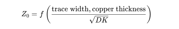
In any RF PCB material used for wireless modules, radar systems, or 5G designs, few parameters influence performance as strongly as DK, or dielectric constant. When engineers talk about controlled impedance PCB structures, DK sits at the heart of every decision. It shapes signal speed, impedance behavior, and even how your RF transmission line behaves at microwave frequencies.
If your goal is stable, predictable high-frequency PCB design, understanding why DK matters will help you choose better laminates and avoid costly tuning steps.
DK Directly Determines the Impedance of RF Transmission Lines
Every RF microstrip impedance calculation depends on DK. The material’s dielectric constant feeds into the formula that sets the final impedance for 50Ω microstrip lines, 75Ω video lines, and many custom RF structures.
The relationship is simple:
Higher DK → lower impedance
Lower DK → higher impedance
This is why RF PCB stack-up design can only be accurate when the underlying DK is consistent. Even a small DK shift, such as ±0.1, can move the impedance by several ohms. At microwave frequencies, that difference influences return loss, matching accuracy, and the stability of filters or antennas.
To reduce this variation, engineers often choose Rogers RF materials such as RO3003, RO4003C, and RO4350B, which maintain tighter DK tolerance than conventional FR4.
DK Stability Protects RF Circuits From Impedance Drift
Standard materials, such as FR4, show large DK swings at different frequencies and temperatures. But advanced high-frequency laminate materials are engineered for stability across environmental changes, humidity, and frequency ranges.
Stable DK provides stable impedance, which leads to:
cleaner signal flow
predictable matching in RF front-end circuits
stable phase length for microwave structures
consistent RF PCB routing performance
For microwave builds, especially above 2–3 GHz, DK tolerance becomes one of the clearest indicators of high-quality RF PCB material selection.
DK Controls RF Signal Propagation
Impedance is not just a number—it reflects how electromagnetic energy moves across the PCB. DK defines the relationship between the electric field in the trace and the dielectric beneath it. When DK is stable, signal propagation speed stays stable too.
This affects many RF structures:
microstrip antennas
transmission lines for mixers, LNAs, and PAs
VCOs and PLL circuits
bandpass filters and couplers
phased-array elements
radar transceiver lines
With stable DK, these structures behave closer to their modeled performance, reducing the risk of frequency drift or unexpected resonance shifts.
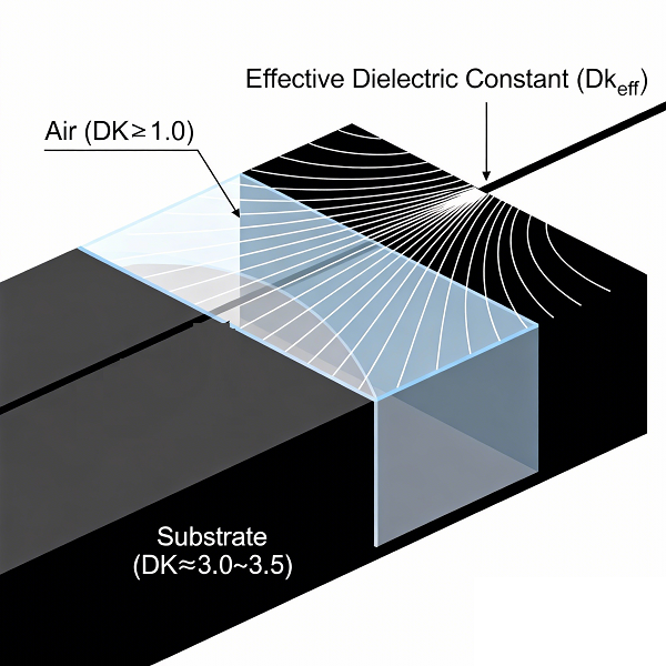
DK Influences Effective Permittivity (Dk_eff)
Most RF layouts use microstrip or grounded CPW traces, where only part of the electromagnetic field flows inside the substrate. The remaining field propagates through the air. The combined effect is called the effective dielectric constant (εeff) or Dk_eff.
Because Dk_eff sits between the substrate DK and air’s DK (≈1.0), any movement in the substrate DK shifts the effective value.
That creates changes in:
impedance
phase velocity
electrical length of the line
signal wavelength on the PCB
coupling between adjacent structures
For this reason, impedance-controlled PCBs for RF applications require laminates with tight DK tolerance across the panel and across the entire RF stack-up.
Tight DK Tolerance Reduces Prototyping Time
When using predictable materials, simulation models match real PCB results more closely. Designers experience fewer tuning cycles, fewer redesigns, and faster production.
Consistent DK helps:
improve RF yield
reduce tuning in power amplifier bias lines
support repeatable RF PCB manufacturing
make stack-up calculations more accurate
This is especially valuable in industries like automotive radar, satellite communication, low-noise amplifier design, and compact 5G modules.
DK Variation Increases Reflection and Mismatch Loss
Loss tangent (Df) defines dielectric loss, but DK variation introduces mismatch loss. When impedance deviates from the intended value, part of the RF signal reflects back toward the source, reducing forward transmission.
Effects include:
higher insertion loss
increased ripple in filters
degraded VSWR
phase errors in antenna arrays
unwanted standing waves
Stable DK helps avoid these issues by keeping impedance as close as possible to its original design target.
DK and RF PCB Stack-Up Selection
A high-performance RF PCB stack-up design always begins with DK. Engineers set copper thickness, dielectric thickness, and trace geometry around it. RF stack-ups with predictable DK behave consistently across production batches, which keeps high-volume runs stable.
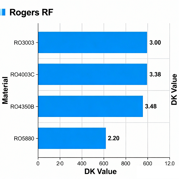
Popular RF materials selected for stable DK include:
Rogers RO3003 (DK ≈ 3.00 ± 0.04)
Rogers RO4350B (DK ≈ 3.48 ± 0.05)
Rogers RO4003C (DK ≈ 3.38 ± 0.05)
Rogers RO5880 (DK ≈ 2.20 ± 0.02)
Taconic RF-35, TLY, and other PTFE-based laminates
These laminates are widely used in microwave designs because they give designers the confidence that impedance and electrical length stay predictable across builds.
Why DK Matters Even More Above 10 GHz?
As frequencies extend toward mmWave ranges, minor DK deviations introduce major impedance shifts. The higher the operating frequency, the more sensitive impedance becomes to dielectric constant variations.
For example:
At 1–2 GHz, DK tolerance of ±0.05 produces measurable but manageable impact.
At 10–24 GHz, the same DK deviation causes more dramatic impedance changes.
Above 28–39 GHz (5G FR2 bands), DK control becomes one of the most essential parameters in RF material selection.
This is why mmWave PCB manufacturing overwhelmingly relies on PTFE-based or ceramic-filled laminates with extremely tight DK tolerance.
EBest Circuit (Best Technology) – Your Trusted Partner for RF PCB Manufacturing
For designers working on high-frequency and microwave projects, precise DK control is only the starting point. You also need a PCB manufacturer with strong RF engineering experience, stable processes, and a deep understanding of controlled impedance PCB builds. At EBest Circuit (Best Technology), we support global RF teams through:
1. Advanced RF PCB materials – RO3003, RO4350B, RO4003C, RO5880, Taconic, and other high-frequency laminates.
2. Tight impedance tolerance – ±5% impedance control with certified test reports.
3. Professional RF stack-up design assistance – Our engineers help calculate trace widths, dielectric thicknesses, and Dk_eff models for accurate impedance.
5. Rigid quality control – ISO9001, ISO13485, AS9100D, IATF16949, and full MES traceability for all builds.
When your RF design demands precise signal behavior, stable impedance, and reliable material performance, EBest Circuit (Best Technology) provides the expertise and manufacturing strength needed to support advanced RF and microwave innovation.
In RF and microwave PCB materials, DK means Dielectric Constant, also known as relative permittivity (εr).
Designing an RF or microwave PCB involves far more than routing traces—you must understand how materials behave at high frequencies. One of the most critical parameters is DK. Whether you are building a 1 GHz RF amplifier, a 10 GHz radar board, or a 77 GHz millimeter-wave automotive sensor, DK directly affects signal integrity, impedance, and loss.
This guide covers what DK means, why it matters, how it affects impedance, common RF PCB materials and their DK values, and how to choose the right laminate for RF, microwave, and mmWave designs.
Used in ultra-high-frequency and high-reliability applications:
stable DK
low CTE
excellent thermal stability
Applications: Space, military RF systems, phased-array radar.
Here is a summarized RF material parameter:
Material Category
Typical DK
Frequency Use
Notes
FR-4
4.2–4.8
<1 GHz
High loss, unsuitable for RF/microwave
Rogers RO4000 Series
3.27–3.55
1–20 GHz
Cost-effective, stable DK
Rogers RO3000 Series
3.0, 3.38
10–40 GHz
Low loss, mmWave-ready
PTFE (Teflon) laminates
2.17–2.6
up to 60 GHz+
Very low loss, used for 5G & radar
Ceramic-filled laminates
2.2–6.0
up to 77 GHz
Good CTE, stable DK
Typical DK Values of Popular RF PCB Materials
Rogers RO3000 Series
Material
DK @ 10 GHz
Notes
RO3003
3.00 ± 0.04
Excellent for mmWave, 5G, radar
RO3006
6.15
Compact RF components
RO3010
10.2
Miniaturized RF circuits
Rogers RO4000 Series
Material
DK
Notes
RO4003C
3.38
Low-loss, cost-effective
RO4350B
3.48
High-power RF, stable performance
RO4835
3.48
High reliability, PIM stability
PTFE (Duroid) Materials
Material
DK
Notes
RT/duroid 5880
2.20
Super low DK, radar & aerospace
RT/duroid 5870
2.33
Low loss for satellite comms
Why RT5880 is Important for High-Frequency Designs?
RT5880 is especially favored for:
77 GHz automotive radar
Ka-band satellite communications
High-end phased-array antennas
Microwave lenses & radomes
Low-loss RF feed networks
Its ultra-low DK and extremely low loss tangent make it one of the best choices for millimeter-wave and low-loss RF applications.
RF PCBDesign
PCB Material Selection for RF, Microwave & Millimeter-Wave Designs
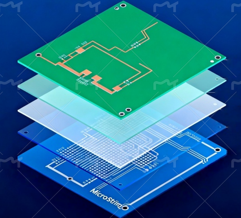
Choosing the right PCB material is one of the most important steps in designing an RF, microwave, or millimeter-wave circuit. At high frequencies, the dielectric constant (DK), dissipation factor (DF), copper type, and thermal stability directly affect signal loss, impedance, and long-term reliability. Below is a practical guide to help you choose the most suitable RF PCB laminate for your frequency and performance requirements.
1. DK Stability Over Frequency and Temperature
In RF systems, DK accuracy and stability are more important than the DK number itself. Materials with unstable DK can cause:
impedance drift
phase delay variation
poor antenna radiation efficiency
frequency shifting in filters and resonators
Choose materials with:
tight DK tolerance (±0.02–±0.04)
low TCDk (temperature coefficient of dielectric constant)
stable DK from 1 GHz up to 40+ GHz
Best choices: Rogers RO3003, RO4350B, RT/Duroid 5880.
2. Loss Performance (Dissipation Factor / DF)
Loss increases rapidly as frequency goes higher. A low DF is essential for maintaining signal integrity at:
Using the right material ensures correct impedance, low loss, and predictable electrical behavior.
So in summary:
To choose the ideal RF PCB substrate, evaluate:
DK accuracy & stability
DF (loss)
copper roughness
CTE & thermal performance
fabrication difficulty
operating frequency
your budget vs performance
For most RF applications (1–20 GHz), RO4003C / RO4350B provide the best balance. For millimeter-wave (24–80 GHz), RT/duroid 5880 or RO3003 deliver superior performance with extremely low loss.
EBest Circuit (Best Technology) provides strong support for RF, microwave, and millimeter-wave PCB production. Our team works with Rogers, Taconic, PTFE, ceramic-filled PTFE, hydrocarbon laminates, and hybrid stack-ups.
Customers value our service because:
We hold ISO9001, ISO13485 for medical, IATF16949 for automotive, and AS9100D for aerospace
We manage full production through MES systems to keep real-time traceability
We support impedance control with stable processes
We produce many RF board types, including RO3003, RO4003C, RO4350B, and RT5880
Our engineers review stack-ups and provide DFM to reduce risk
We offer competitive pricing with consistent quality
EBest Circuit (Best Technology) works closely with RF designers worldwide. We help convert a concept into a stable, manufacturable board. For teams that need stable performance, reliable impedance control, and smooth communication, EBest Circuit (Best Technology) provides a trusted path for RF PCB manufacturing.
FAQs
1. What DK value works well for millimeter-wave PCB design?
Materials like RO3003 or RT/duroid 5880 work well because they keep a steady DK and low loss at high frequencies, which helps the circuit stay stable.
2. Does DK affect RF and microwave filter design?
Yes, DK affects impedance and phase along the line, so a small DK shift can change a filter’s response. A stable DK keeps the filter closer to its intended shape.
3. Why do many antennas use low-DK materials?
Low-DK materials spread the field more evenly and support wider bandwidth, which helps antennas keep stable resonance and steady radiation patterns.
4. Can FR4 work for RF designs?
FR4 can support low-frequency RF work, but its DK drifts with temperature and humidity. Higher-frequency circuits need RF laminates with better DK stability.
5. How does DK influence microstrip impedance?
DK shapes how fast signals move and how fields sit in the dielectric, so higher DK lowers impedance and lower DK raises it. Designers adjust trace width based on this behavior.
Not exactly. All RF PCBs fall under the high-frequency PCB category, but not all high-frequency PCBs qualify as RF PCBs.
RF PCB work sits at the center of many wireless systems, and an RF PCB often looks similar to a high frequency pcb. Many designers ask if they are the same board. They are related, yet each one handles different needs in signal flow, layout control, and material behavior.
As we move deeper into 5G, radar modules, and clean wireless designs, the differences become more visible. This article explains those differences in simple, clear language. More importantly, it guides engineers, buyers, and project teams on how to choose the right board for their next product.
What Is an RF PCB?
An RF PCB full name is Radio Frequency PCB, which is specifically handles signals in the radio frequency range: typically 300 MHz to 300 GHz, including microwave and millimeter-wave designs.
RF PCBs involve much stricter engineering constraints:
Tight impedance (<±5%) on microstrip, grounded CPW, stripline
Precise feature control (trace width tolerance around ±0.01–0.03 mm)
Stable dielectric properties across temperature
Very low-loss materials such as RO3003, RO4350B, RO5880, Taconic RF-35, PTFE woven/non-woven
Specialized stackups to avoid parasitic radiation
Careful via design to avoid stubs and resonance
Applications include:
Radar systems
Satellite communication
LNBs
RF front-end modules
Power amplifiers
Filters, couplers, antennas
RF PCB is wider use of 5G, IoT, and compact antennas has created strong demand for high-grade rf pcb builds. Because the signals travel along microstrip or CPW structures, the board behaves like part of the RF device, not only a carrier.
What Is a High-Frequency PCB?
A high-frequency PCB is any printed circuit board operating above roughly 500 MHz to 10 GHz+, depending on the design community.
Low dissipation factor (Df) for reduced signal loss
Good impedance control across long traces
Suitable materials like Rogers RO4003C, RO4350B, RO3003, PTFE, Isola I-Tera MT40, etc.
High-frequency PCBs serve applications such as:
5G modules
Wi-Fi devices
GPS receivers
High-speed digital layouts (DDR4/DDR5, SerDes)
High frequency boards focus on clean rise times, controlled impedance, and manageable dielectric loss. They support Wi-Fi, Bluetooth, high-speed digital lines, and mixed-signal designs. The design margin is wider than rf pcb work because the board deals with digital pulses, not pure RF energy.
High Frequency PCB
Key Differences Between RF PCB vs. High Frequency PCB
Aspect
High-Frequency PCB
RF PCB
Definition
Boards operating at high digital or analog frequencies
Boards designed specifically for RF signal transmission
The board contains microstrip, CPW, filters, or antennas
For example, a 2.4 GHz RF transceiver board using RO4350B is simultaneously:
a high-frequency PCB, because frequency is high
an RF PCB, because it processes RF signals
Thus, overlap exists, but they are not inherently identical.
Which One Should You Specify to Your PCB Supplier?
If your project handles RF transmission, always specify RF PCB so the manufacturer focuses on:
surface roughness control (Ra < 2 µm for low loss)
uniform dielectric thickness
controlled resin flow during lamination
tighter etching tolerance
Dk matching for microstrip/CPW accuracy
If it is only high-speed digital (e.g., PCIe, SerDes), then choose high-frequency PCB.
Why Do RF PCBs Need Special Materials Compared with High Frequency PCBs?
Material behavior influences both categories. Yet an rf pcb is more sensitive to the dielectric constant and copper profile.
RF units run energy through transmission lines. If the copper roughness increases loss, the system sees reduced range or gain shift. If the Dk drifts, the phase response moves. Because of this, the most common materials for rf pcb work include RO3003, RO4350B, RO5880, and PTFE blends.
In contrast, high frequency pcb materials can include Megtron series or Rogers 4000 series because the signal shape is less sensitive to phase stability. They still target low loss, but their working window is wider.
What Frequencies Define RF PCB Work vs High Frequency PCB Work?
Both ranges relate to how the signal behaves. RF work usually starts at 300 MHz and goes up to millimeter-wave. This includes radar, satellite, GPS, 24 GHz and 77 GHz systems, and many short-range radios.
High frequency ranges start from about 500 MHz to beyond 10 GHz. These support fast digital buses, Wi-Fi, and mixed-signal designs.
However, the frequency alone does not decide the board’s category. The final system function does.
Do RF PCBs Always Cost More Than High Frequency PCBs?
Actually yes when under the same design. RF boards use premium materials. These materials cost more because they hold stable Dk, low loss, and a smooth copper surface. They also require strict process control during drilling, plating, and lamination.
High frequency boards may use moderate-cost materials such as RO4003C or Megtron 4. They also need controlled lamination, yet the window for yield is wider.
Costs also rise when an rf pcb uses fine lines, tight impedance, or stacked microstrip structures. That said, skilled manufacturers can keep RF costs under control by optimizing stackup and process flow.
What Problems Occur When Designers Use the Wrong PCB Type?
If a design intended for RF is built on a standard high frequency pcb, several issues may appear:
Reduced communication range
Higher insertion loss
Unstable gain
Incorrect antenna tuning
Phase delay changes
EMC issues
Although not every situation is severe, these issues waste time in testing and rework.
When a high frequency digital board is produced using strict RF rules, the design remains stable. Yet the cost often rises without a visible performance gain.
What Tests Are Important for RF PCBs Compared with High Frequency PCBs?
RF boards often need tests beyond regular PCB checks. These include:
Dielectric thickness check
Dk variation review
Copper profile check
TDR impedance scan
S-parameter review after assembly
High frequency boards may also use TDR scans, yet the tolerance is wider. For RF, every shift affects the final device.
How Does EBest Circuit (Best Technology) Support RF PCB and High Frequency PCB Projects?
EBest Circuit (Best Technology) offers full material guidance, stackup review, transmission line advice, and strong quality assurance for both rf pcb and high frequency pcb builds. We handle small prototype lots and volume orders with the same care. Each rf pcb passes a detailed review, so the final product meets the performance target.
Our strengths include:
ISO9001, ISO13485, IATF16949, and AS9100D systems
Complete MES traceability
Tight impedance control
Fine etching for RF lines
Skilled process teams for PTFE and hybrid stackups
Smooth copper profile management
Fast prototype to mass build for global clients
We support antenna work, radar modules, filters, amplifiers, and mixed-signal boards. Our engineering team reviews each design before production to catch layout risks early to speed up product launches. For your next RF or high frequency project, our team stands ready to guide you from concept to delivery!
FAQs
1. Is an rf pcb the same as a high frequency pcb?
No. All RF boards are high frequency boards, but not all high frequency boards meet RF conditions.
2. Can I use RO4003C for both RF and high frequency PCB use?
Yes. However, many RF systems still need lower-loss materials such as RO3003 or RO5880.
3. Are RF boards harder to build?
Yes. They need tighter process control, smoother copper, and stable lamination.
4. How do I know if my design needs an rf pcb?
If your design uses antennas, filters, couplers, or PA modules, you need an RF board.
5. Does EBest Circuit (Best Technology) support RF and high frequency PCBA work?
Yes. We handle full assembly, tuning, connector installation, and testing.
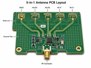
When it comes to wireless systems—WiFi, Bluetooth, cellular IoT, radar, GPS, or any RF module—the performance of the radio frequency PCB (RF PCB) directly determines signal integrity, radiation efficiency, and product stability. A radio frequency PCB operates in high-frequency environments where small layout changes may shift impedance, weaken gain, or create unwanted noise. Because of this, a radio frequency PCB requires strict engineering rules, carefully selected materials, and a routing method that protects signal quality.
This article explains what an RF PCB is, the characteristics you must consider, the right FR PCB materials, the correct RF PCB routing rules, and a complete RF PCB design guideline you can follow for your next high-frequency design. Hope this guide is helpful and give you a best solution to design your RF PCB.
What Is a Radio Frequency PCB?
A radio frequency PCB, or RF PCB, refers to a board used to transmit and receive signals at high frequencies—from hundreds of megahertz to multiple gigahertz. These boards are widely used in wireless modules, IoT devices, GPS systems, consumer electronics, radar sensors, and communication infrastructure.
Unlike standard FR4 boards, RF PCBs involve dedicated dielectric materials, controlled impedance structures, and strict layout rules to keep signal integrity stable. The entire PCB—from stack-up to routing—must support predictable propagation velocity, stable loss characteristics, and smooth energy flow.
RF PCBs are used in:
Wireless modules
GPS receivers
Sub-GHz transmitters
5G communication units
Radar sensors
IoT devices
RF amplifiers and mixers
Antenna feed circuits
Their performance depends on trace geometry, ground stability, and how cleanly the RF path is designed.
What Is a Radio Frequency PCB?
Characteristics of an RF PCB
RF PCBs typically have the following characteristics:
Controlled impedance routing for RF signal paths
Low-loss PCB materials to minimize attenuation
Stable dielectric constant (Dk) over temperature and frequency
Special treatment around matching networks and antenna feeds
Because RF energy behaves like waves rather than simple electrical current, the PCB becomes part of the RF system itself—meaning the layout, stack-up, and materials must be engineered for high-frequency behavior.
What Is the Frequency Range of RF PCB?
RF PCBs typically operate in the following ranges:
Frequency Band
Range
Typical Applications
Low RF
300 MHz – 1 GHz
ISM band, sub-GHz transmitters
Mid RF
1 GHz – 6 GHz
Wi-Fi, Bluetooth, GPS
High RF
6 GHz – 30 GHz
5G, radar
Millimeter Wave
30 GHz – 80 GHz
Automotive radar, high-speed links
Most IoT devices today (BLE, WiFi, Zigbee, Sub-GHz RF) fall between 433 MHz – 6 GHz.
What Is the Best PCB Material for RF?
Choosing the right laminate affects signal quality, trace accuracy, and overall loss.
FR4 PCB Material
FR PCB material, typically FR4, works for low-frequency RF designs below 2.4 GHz. It offers low cost and good mechanical strength. However, its dielectric properties vary with temperature and frequency. Loss tangent is higher than PTFE, so it works best for short RF paths or low-power consumer wireless modules.
Rogers RF Materials
Rogers laminates such as RO4350B, RO4003C, and RO5880 are widely used for RF designs due to:
Low loss tangent
Very stable dielectric constant
Smooth copper surface
High processing consistency
These materials are ideal for GPS, radar, Wi-Fi 6, UWB, sub-6G, and millimeter-wave applications.
PTFE / Teflon Laminates
PTFE offers excellent RF performance, especially for microwave and radar. It has very low loss and highly stable characteristics. Fabrication needs tight process control due to soft substrate behavior.
Ceramic Substrates
Ceramics substrate provide strong thermal stability and high dielectric precision. They work well in high-power RF amplifiers, satellite communication modules, and advanced radar systems.
Here is a common radio frequency PCB material table:
Substrate
Tg (°C)
Td (°C)
Dk
Loss Tangent
Band
FR4
~135
~295
< 4.4
~0.022 (parasitic ignored)
X–K
Isola MT40
200
360
3.38–3.75
0.0028–0.0035
W
IS680 AG-348
200
360
3.48
0.0029
W
IS680 AG
200
360
3.00–3.48
0.0020–0.0029
W
IS680
200
360
2.80–3.45
0.0025–0.0035
W
Isola MT77
200
360
3.00
0.0017
W
Rogers 3003
NR
500
3.00
0.0013
W
Rogers 3006
NR
500
6.15
0.0022
X–Ka
Rogers 4360
>280
407
6.15
0.0038
X–Ka
RT Duroid 6010.2LM
NR
500
10.70
0.0023
X–Ka
RT Duroid 6202
NR
500
2.90
0.0015
X–Ka
RT Duroid 6006
NR
500
6.45
0.0027
X–Ka
RT Duroid 6035
NR
NR
3.50
0.0013
X–Ka
(Note: NR means Not Reported)
PCB Design Guide for Radio Frequency RF Boards
Designing RF PCBs involves stack-up planning, controlled impedance, grounding, spacing, matching networks, and EMI reduction. Below are the recommended RF PCB guidelines and routing rules you can apply to achieve stable wireless performance.
1. Start With Complete RF Design Information
Successful RF PCB design begins long before the first trace is drawn. Engineers must collect all essential RF parameters to avoid redesigns later. This includes:
Functional description and operating frequency band
Current and voltage requirements of each RF stage
RF component list and package dimensions
PA gain, receiver sensitivity, and system isolation targets
Planned PCB stack-up structure
Controlled impedance values
Mechanical constraints and enclosure limits
Shielding frame or metal-can dimensions
Matching network reference designs
Simulation results for power amplifiers and LNAs
Gathering this information early ensures that layout decisions align with system-level RF performance.
PCB Design Guide for Radio Frequency RF Boards
2. Physical Zoning of the RF PCB
Physical zoning organizes the board according to how RF signals flow.
RF Signal Flow Placement
Place RF components in the exact order of the signal chain. A short, direct, and linear path minimizes insertion loss, improves impedance stability, and preserves gain.
RF Component Orientation
Rotate filters, PAs, LNAs, couplers, and mixers so their input/output pins align with the straightest possible RF path. Avoid unnecessary detours or bends.
Isolation Through Ground Structures
To prevent RF coupling and cross-interference, isolate RF sections using:
Ground shielding walls
Via-fence structures
Shield cans over sensitive circuits
Copper barriers or partitions
These structures keep RF and digital noise apart, improving overall stability.
3. Electrical Zoning
Electrical zoning separates different circuit domains so they cannot interfere with each other.
Power section: Power management ICs, regulators
Digital control section: MCUs, logic circuits, clocks
Analog RF section: LNAs, PAs, filters, mixers, antennas
These zones should not overlap in routing. Digital switching noise or PLL jitter can easily couple into RF paths if the layout is not properly divided.
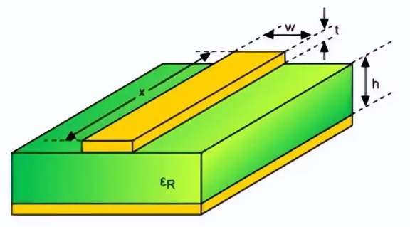
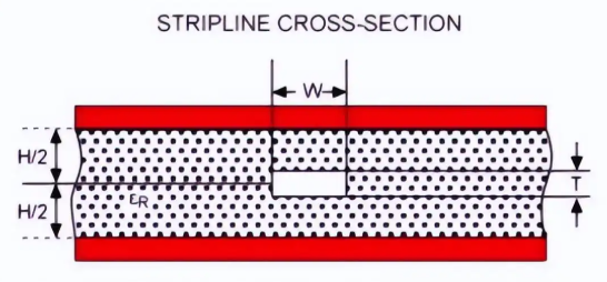
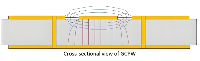
4. RF Transmission Line Structures
RF PCBs commonly use one of three controlled-impedance transmission line types:
Impedance determined by trace width and dielectric height
Ideal for simple and low-to-mid–frequency RF designs.
Stripline
RF trace routed on an inner layer
Sandwiched between two solid ground planes
Provides superior isolation and uniform impedance
Useful in compact or high-frequency designs where shielding is critical.
Grounded Coplanar Waveguide (GCPW)
Top-layer trace with ground on both sides
Ground plane below the trace
Excellent isolation and impedance control
Often preferred when space is tight or when multiple RF lines run in parallel.
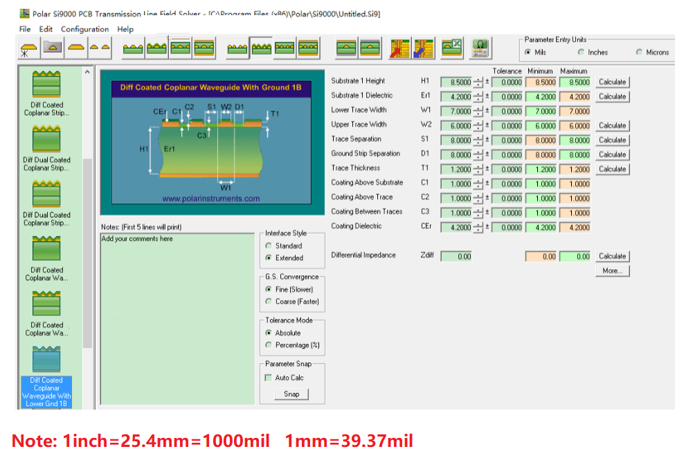
5. Impedance Selection and Calculation
Achieving the correct characteristic impedance (typically 50Ω) requires considering:
Trace width
Copper thickness
Dielectric constant (Dk)
Dielectric height between layers
Use tools such as Polar SI9000 or your PCB manufacturer’s impedance calculator.
6. RF Trace Bending Rules
Straight RF traces are ideal, but bends are sometimes unavoidable.
Follow these rules:
Minimum bend radius ≥ 3× trace width
Avoid 90° bends (cause impedance discontinuity)
Use 45° bends or smooth arc/bowed shapes
Apply mitering to compensate for impedance changes
For critical RF links, simulate bends in an EM solver to validate performance.
7. Layer Transitions for RF Traces
RF traces should stay on one layer. If a layer change is unavoidable:
Use two vias at minimum
Via diameter should match the RF trace width
When space is tight, use three smaller vias in parallel
Multiple vias reduce via inductance and minimize impedance mismatch.
8. Signal Isolation Rules
Isolation is as important as impedance control in RF design.
a)RF Lines
Keep RF traces well separated
Avoid long parallel runs
Use GCPW for noisy or densely packed areas
Keep sensitive microwave lines away from high-power circuits
b)High-Speed Digital Signals
Route digital clocks on different layers
Avoid crossing beneath RF paths
Switching noise can modulate RF signals if not isolated
c) Power Lines
Use a dedicated power layer for stable distribution
Place bypass capacitors close to RF IC power pins
Keep power traces away from RF transmission lines
9. Ground Area Design
Ground integrity determines the quality of RF performance.
Use solid, continuous ground planes
Avoid slots, gaps, and return-path interruptions
Do not route signals across RF ground regions
Add abundant ground stitching vias
Reduce inductance in ground loops
In RF PCB design, a 4-layer RF PCB design is widely considered the most balanced structure for modern wireless modules because it provides stable impedance, strong isolation, and efficient routing without dramatically increasing manufacturing cost. While 2-layer boards are cheaper and 6-layer boards offer more routing space, the 4-layer stack-up delivers the best performance-to-cost ratio for most RF applications under 6 GHz.
Layer 3 (Power Plane): Power routing + local shielding below RF areas
Layer 4 (Bottom Layer): Non-critical routing or power distribution
RF PCB Routing Rules You Must Follow
1. The length of the RF traces should be kept as short as possible, and ensure that the surrounding densely arranged holes are shielded. The intervals should be approximately 50 mils.
2. RF traces must not have vias, meaning they cannot cross layers. It is preferable to use 135° angle traces or circular traces.
3. Near the RF traces, there should be no high-frequency signal lines. Pay attention to the UART signal line being shielded by a ground layer, and add ground holes around it for protection.
4. The RF traces should be as close as possible to the size of the pads.
5. For the RF traces, matching networks and the area around the antenna socket > 0.8mm, copper cannot be laid; they need to be hollowed out.
6. The RF traces should be kept as far away from the battery holder as possible, with a distance of at least 5mm or more.
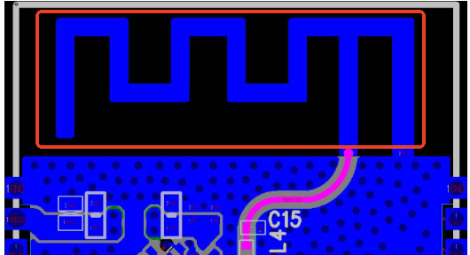
7. A π-type matching circuit needs to be reserved on the RF path, and this π-type matching circuit should be placed close to the chip end like below diagram show:
IPC Standards for Radio Frequency PCB
The following IPC standards are typically referenced for RF PCB and high-frequency designs:
IPC-6018 – Qualification and Performance Specification for High Frequency (Microwave) PCBs
IPC-2221/2222 – General & rigid PCB design rules
IPC-2141 – Controlled impedance design
IPC-TM-650 – Test methods for dielectric materials
IPC-4103 – High-frequency base materials
These standards help ensure reliability, board performance, and manufacturability for RF and microwave applications.
Your Reliable RF PCB Manufacturer – EBest Circuit (Best Technology)
Best technology is an experienced RF PCB manufacturer in China, we offer stack-up consultation, material selection, transmission line simulation, and impedance guidance for complex RF modules. Our production lines use SI9000 modeling, fine etching control, and well-controlled lamination parameters. Our radio frequency PCB manufacture capability including:
Rogers, SY, Isola, PTFE, and hybrid RF PCB materials
Tight-tolerance controlled impedance
4–10 layer high-frequency stack-ups
Laser drilling, buried/blind vias
Ceramic-filled dielectric PCB options
Full DFM & design support for RF modules and antennas
In addition to this, we offer one-stop PCB & PCBA service covers RF tuning, antenna matching, shielding assembly, coaxial connector installation and final functional RF tests.
Whether you’re building Bluetooth modules, RF front ends, radar circuitry, or custom antennas, our engineering team ensures high yield and reliable RF performance—helping you bring your wireless product to market faster.
FAQs about RF PCBs
1. What materials are recommended for radio frequency PCB?
Rogers RO4350B, RO4003C, RO5880, PTFE, and high-stability ceramics work best for RF or microwave applications.
2. Can I use FR4 for RF PCB?
Yes, if the operating frequency is low and the RF path is short. Many 433 MHz and 2.4 GHz consumer modules still use FR4.
3. Why should RF traces avoid vias?
A via adds inductance and disrupts impedance. RF energy prefers a continuous layer.
4. What routing structure is most common?
Microstrip and grounded coplanar waveguide are widely used due to predictable impedance.
5. Does EBest Circuit (Best Technology) support RF PCBA assembly?
Yes, including antenna tuning, shielding, coaxial connector mounting, and final RF testing.
This website uses cookies to enhance your experience, remember your preferences, and help us understand how visitors use our site. You can accept all cookies, reject non-essential cookies, or manage your settings.
This website uses cookies to improve your experience while you navigate through the website. Out of these cookies, the cookies that are categorized as necessary are stored on your browser as they are essential for the working of basic functionalities of the website. We also use third-party cookies that help us analyze and understand how you use this website. These cookies will be stored in your browser only with your consent. You also have the option to opt-out of these cookies. But opting out of some of these cookies may have an effect on your browsing experience.
Necessary cookies are absolutely essential for the website to function properly. These cookies ensure basic functionalities and security features of the website, anonymously.
Cookie
Duration
Description
cookielawinfo-checkbox-analytics
11 months
This cookie is set by GDPR Cookie Consent plugin. The cookie is used to store the user consent for the cookies in the category "Analytics".
cookielawinfo-checkbox-functional
11 months
The cookie is set by GDPR cookie consent to record the user consent for the cookies in the category "Functional".
cookielawinfo-checkbox-necessary
11 months
This cookie is set by GDPR Cookie Consent plugin. The cookies is used to store the user consent for the cookies in the category "Necessary".
cookielawinfo-checkbox-others
11 months
This cookie is set by GDPR Cookie Consent plugin. The cookie is used to store the user consent for the cookies in the category "Other.
cookielawinfo-checkbox-performance
11 months
This cookie is set by GDPR Cookie Consent plugin. The cookie is used to store the user consent for the cookies in the category "Performance".
viewed_cookie_policy
11 months
The cookie is set by the GDPR Cookie Consent plugin and is used to store whether or not user has consented to the use of cookies. It does not store any personal data.
Functional cookies help to perform certain functionalities like sharing the content of the website on social media platforms, collect feedbacks, and other third-party features.
Performance cookies are used to understand and analyze the key performance indexes of the website which helps in delivering a better user experience for the visitors.
Analytical cookies are used to understand how visitors interact with the website. These cookies help provide information on metrics the number of visitors, bounce rate, traffic source, etc.
Advertisement cookies are used to provide visitors with relevant ads and marketing campaigns. These cookies track visitors across websites and collect information to provide customized ads.