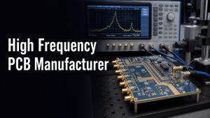
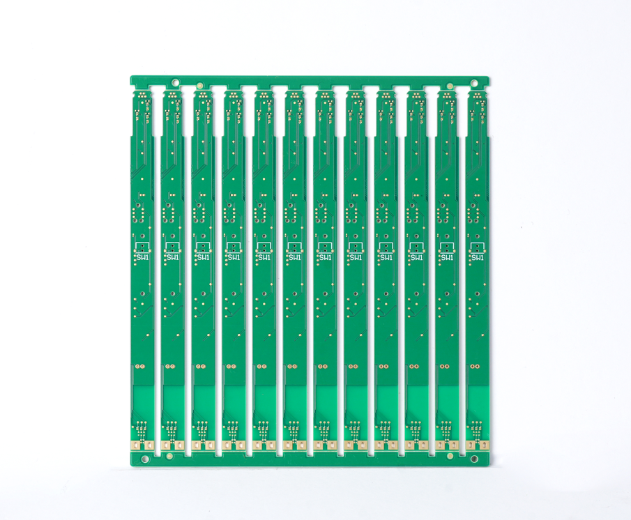
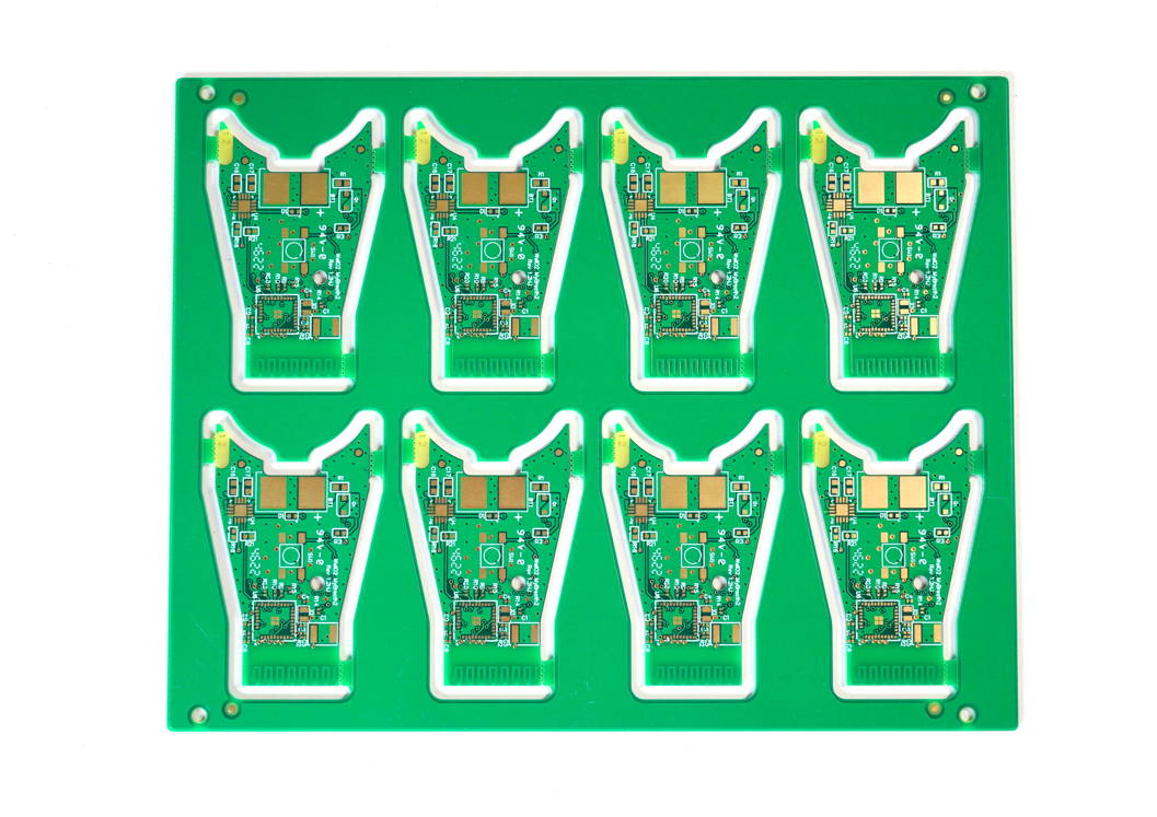
A high frequency PCB manufacturer should understand RF materials, controlled impedance, low-loss stackups, copper treatment, dimensional control, testing expectations and DFM review before quoting the board. The buying risk is not only price. A supplier may quote the board as if it were a standard FR-4 PCB, then discover material, impedance, via, grounding or verification problems after the order is already moving.
This guide explains how to evaluate a high frequency PCB supplier, which technical details affect cost and quality, and why EBest Circuit should be added to your RFQ shortlist early when you need RF material review, DFM feedback, PCB fabrication, PCBA support and production planning.
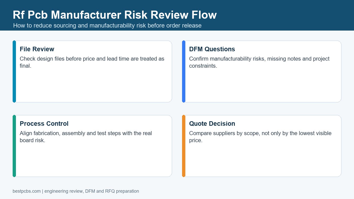
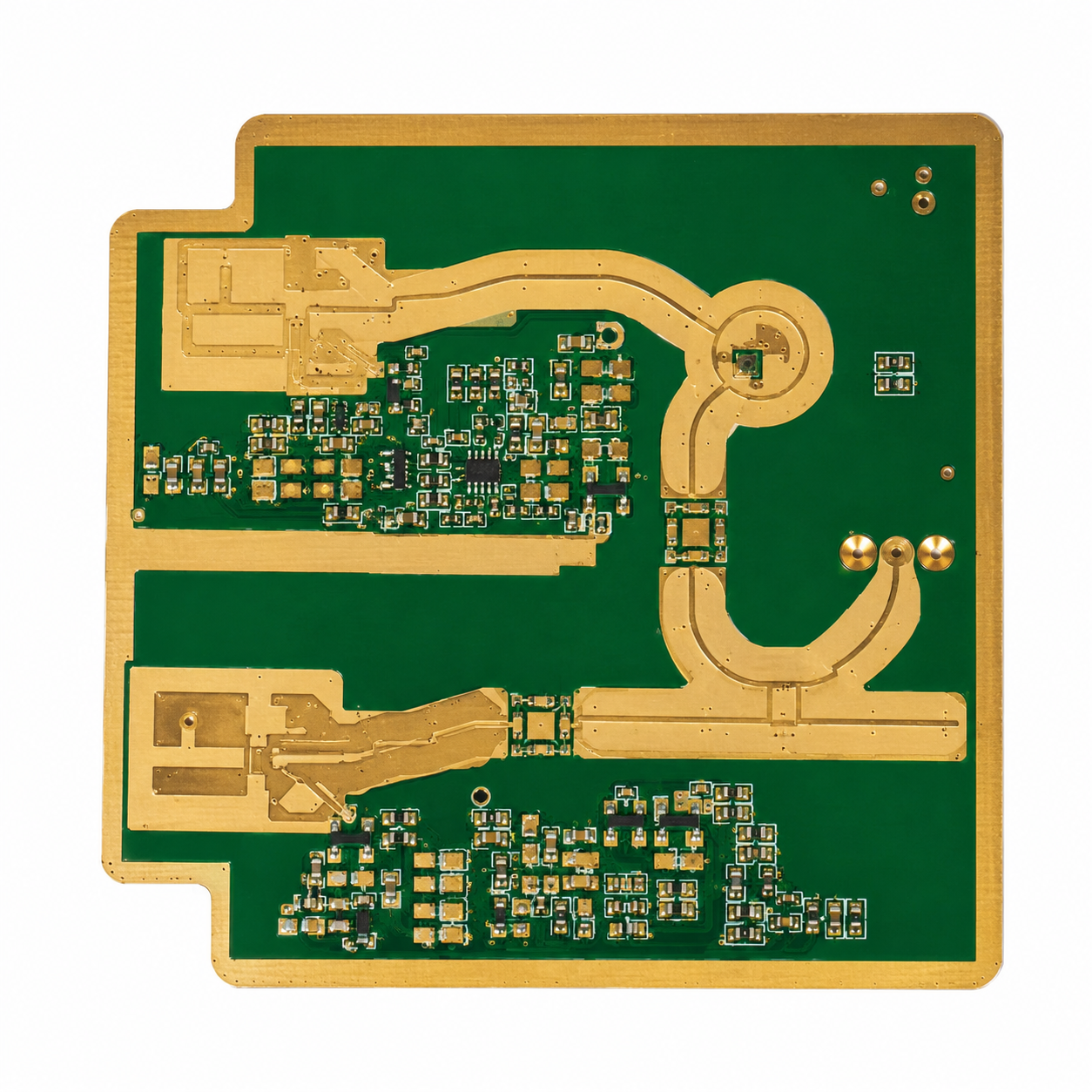
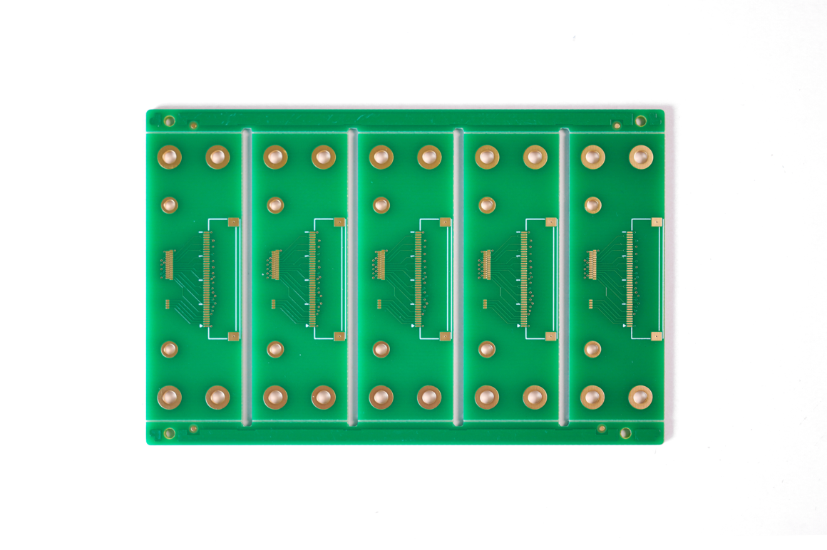
High Frequency PCB Manufacturer at a Glance
The right high frequency PCB supplier should quote the board as an RF or microwave engineering build, not as a generic FR-4 PCB with a different keyword. The buyer should provide material expectations, stackup, impedance targets, frequency range, copper requirements and test needs early.
| Area | What to confirm | Why it matters |
|---|---|---|
| Material | RF laminate, high-speed laminate or hybrid stackup | Loss, stability and manufacturability depend on material choice. |
| Stackup | Reference planes, dielectric thickness and impedance targets | High frequency behavior depends on geometry, not only copper routing. |
| Manufacturing | Drilling, registration, copper finish, etching and dimensional control | Small deviations can change RF performance. |
| Testing | Electrical, impedance, coupon, functional or RF test scope | The buyer must know what the supplier can verify before shipment. |
Have You Run Into These High Frequency PCB Manufacturing Problems Before?
A high frequency PCB quote can look complete while the real RF risk is still hidden in the material, stackup, impedance or test plan.
Many high frequency PCB delays do not start because the board is impossible to build. They start because the RF-sensitive details are confirmed too late, after the buyer has already approved the quote or released the next build.
- The quote names an RF material, but not the real performance target. Buyers may see Rogers, PTFE, Taconic or another laminate name in the discussion, while Dk/Df, frequency range, insertion loss, thickness and availability are still not tied to the actual design.
- The impedance value is stated, but the stackup is not locked. A 50 ohm or differential impedance target can become unclear if dielectric thickness, copper weight, trace width, spacing, plating growth and etch compensation are not reviewed together.
- The factory changes trace width or stackup after the designer has already calculated the RF geometry. Small changes can be acceptable, but only when the buyer understands why they are needed and approves the updated manufacturing stackup before production.
- The prototype works, but the buyer still cannot trust the next production batch. If copper roughness, surface finish, material batch, coupon location or impedance report expectations are not discussed, a sample can pass basic checks while repeatability remains uncertain.
- RF launch, via, grounding and return-path details are treated like normal routing. Connector areas, transitions, reference planes and via structures can affect RF behavior even when the Gerber files pass ordinary fabrication checks.
- The RFQ says ?tested,? but does not define what tested means. Buyers may expect impedance, TDR coupon data, electrical test, functional checks or customer-defined inspection, while the supplier only includes standard checks.
How EBest Circuit helps turn a high frequency PCB RFQ into a clearer manufacturing plan
- Reviews Gerber/ODB++, stackup, drill data, frequency range, material targets, impedance notes, copper requirements, surface finish and testing expectations before confirming the quote path.
- Checks whether the requested material can match the project goal and available high frequency material options. Company capability data includes Rogers 4003 / 4350 / 5880, Taconic laminates, PTFE, Isola 370HR / FR408HR, Nelco and high Tg FR4 options, subject to project confirmation.
- Confirms which impedance details need buyer approval before production, including stackup, trace geometry, copper assumptions, tolerance target and whether an impedance report or coupon check is required.
- Reviews RF-sensitive details such as launch areas, vias, grounding, reference planes, connector placement and layer transitions during DFM so the board is not treated like a standard low-speed PCB.
- When PCBA is required, checks BOM, CPL, assembly drawings, connector placement, handling expectations and inspection needs together with the bare board build.
- Helps buyers compare real manufacturing risk, DFM depth, cost, quality requirements and delivery planning before the next prototype, pilot run or production order is released.
Ready to Build Your High Frequency PCB?
Send your Gerber/ODB++, stackup, impedance notes and BOM for engineering review and practical RFQ feedback.
✓ Free DFM review · ✓ RF material check · ✓ PCB + PCBA support
High Frequency PCB Buyer Priorities Before Quote
High frequency PCB buyers should confirm RF material, stackup, impedance targets, copper details, via structure, surface finish and test expectations before approving a supplier quote. A board can look manufacturable while still carrying RF performance risk.
Send the frequency range, dielectric requirements, impedance notes, Gerber or ODB++ files, drill data and test expectations with the RFQ. This gives the supplier enough context to review the project before production begins.
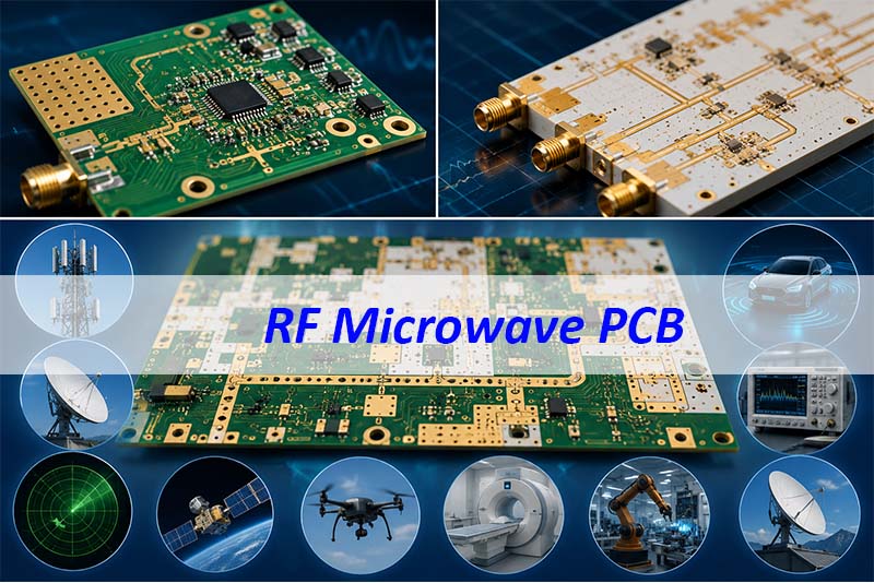
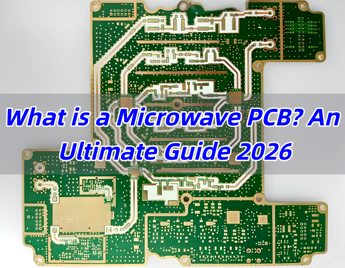
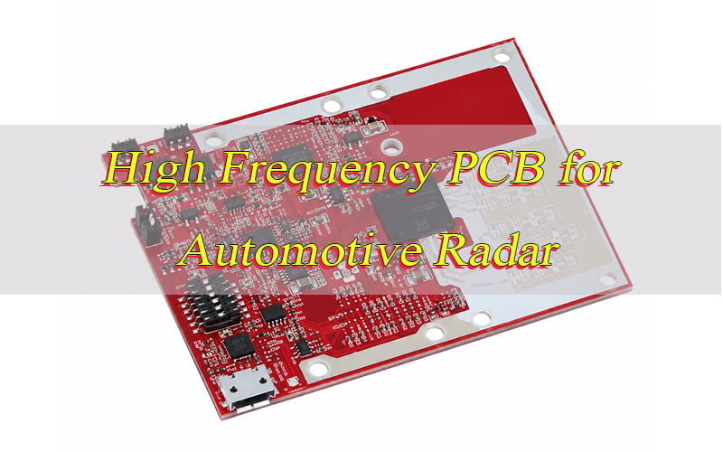
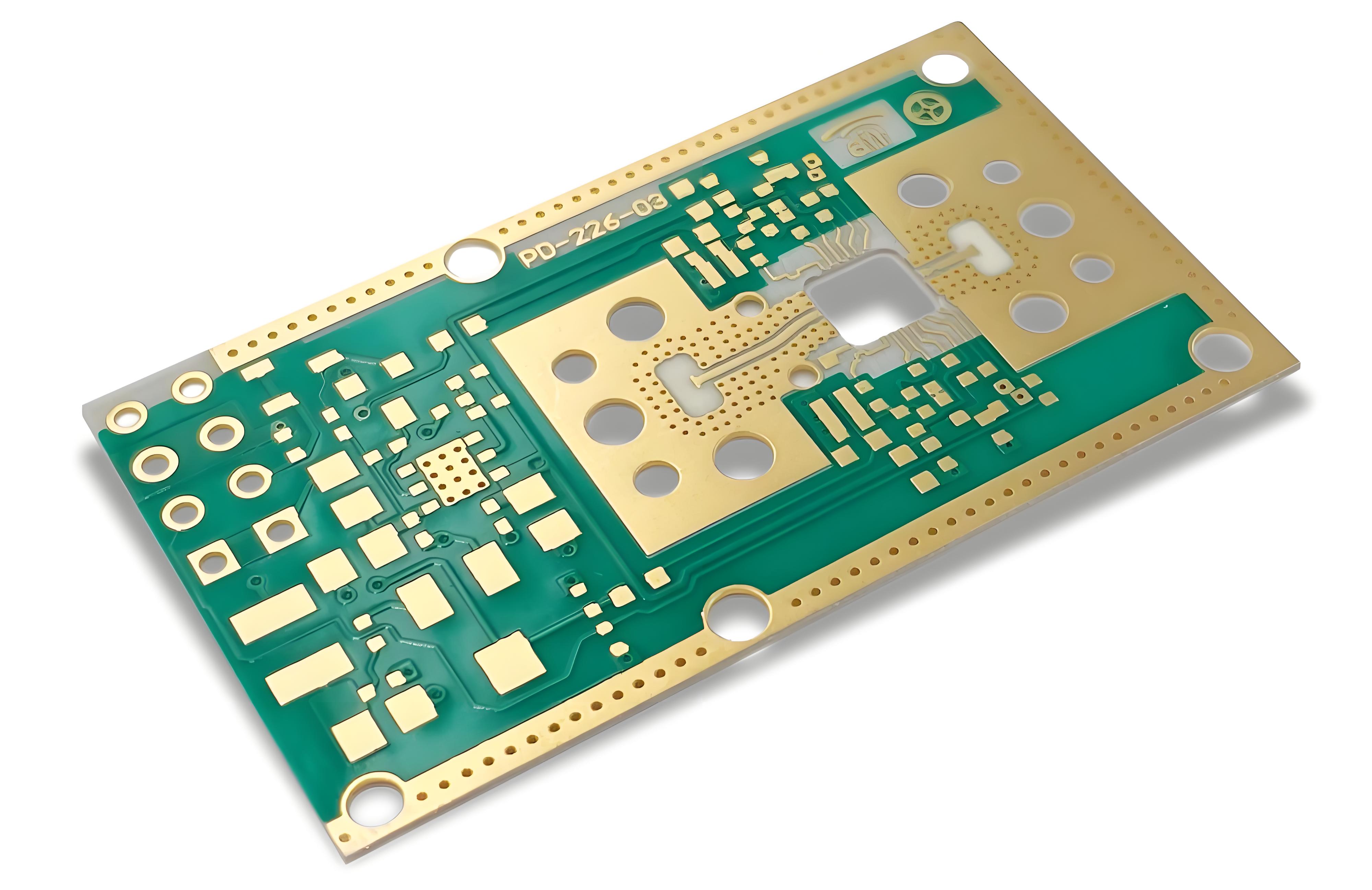
What Counts as a High Frequency PCB?
A high frequency PCB is a circuit board designed for RF, microwave or high-speed signal behavior where material loss, impedance, dielectric stability and geometry control matter. There is no single buying rule that fits every board, so the project files and intended signal behavior must be reviewed.
For a closely related topic, compare this guide with the RF PCB manufacturer RFQ guide.
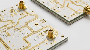
Materials Used in High Frequency PCB Manufacturing
Material selection is one of the first decisions because high frequency behavior is directly affected by dielectric properties, loss and thickness control. Buyers may specify an RF laminate, a high-speed material, a hybrid stackup or a supplier-recommended material after review.
Do not publish a material claim into the order unless it is confirmed in the RFQ and latest process capability data. If the material is a target rather than a requirement, say so and ask the supplier to confirm availability and manufacturability.
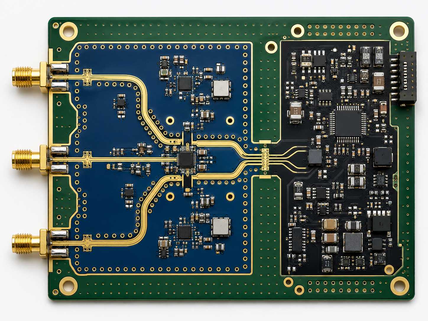
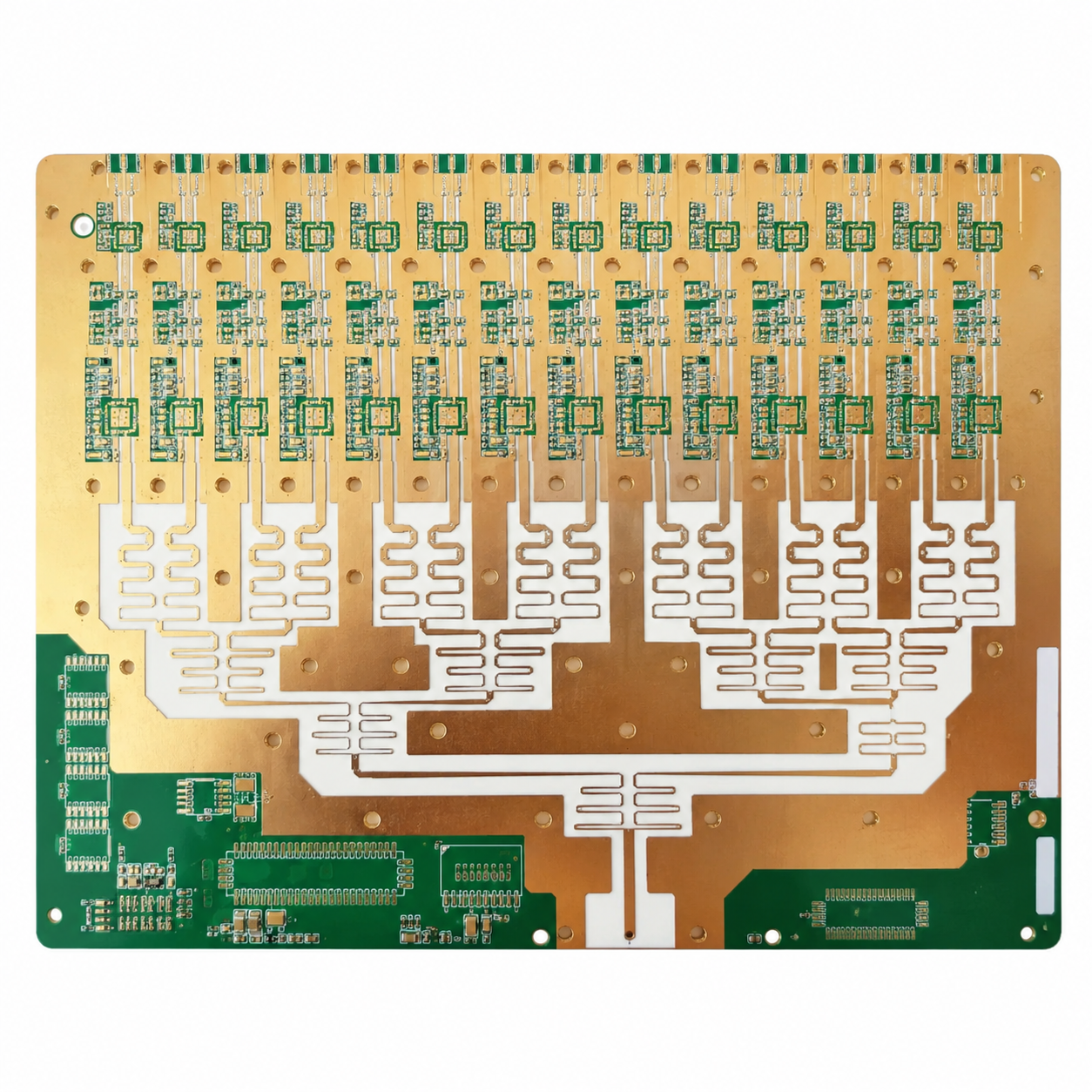
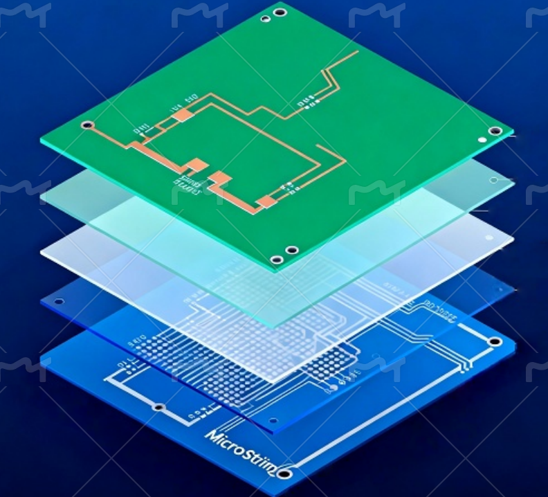
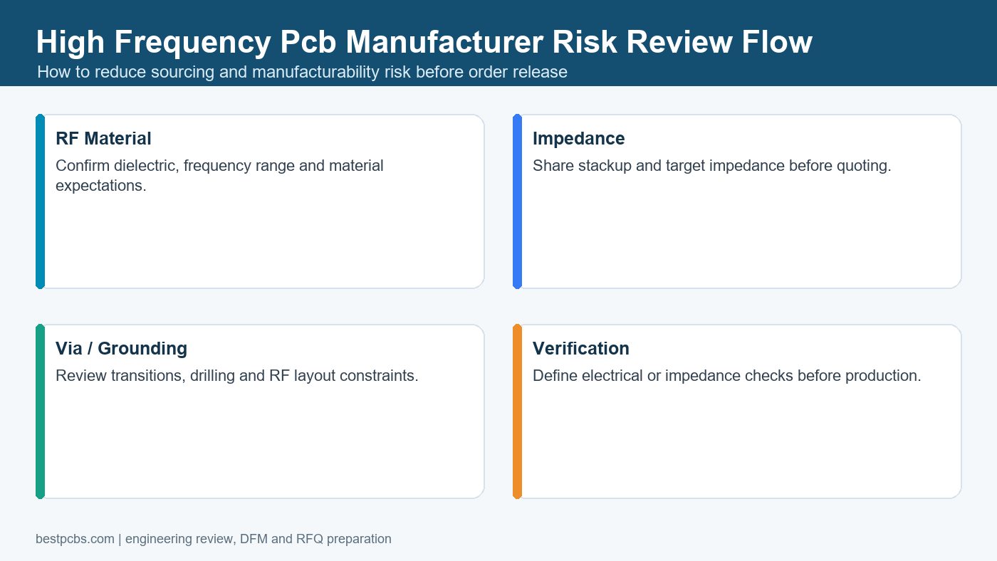
Impedance, Stackup and RF Layout Notes
Controlled impedance and stackup requirements should be written in the fabrication package, not inferred from the copper artwork alone. High frequency layouts often depend on trace width, dielectric thickness, copper roughness, return paths, via transitions and connector launches.
- State impedance values and tolerance requirements.
- Provide stackup targets and reference plane expectations.
- Identify RF traces, antennas, filters, feed lines and connector areas.
- Clarify whether impedance coupons or RF tests are required.
- Separate ordinary control circuitry from RF-sensitive sections.
DFM Review for High Frequency PCBs
DFM review should catch manufacturing changes that could alter RF performance before the order is released. The review should cover material, drill sizes, annular rings, copper features, solder mask openings, panelization, controlled impedance notes and special process instructions.
If the board also needs ordinary design checks, use the PCB design and manufacturing DFM guide alongside the RF-specific review.
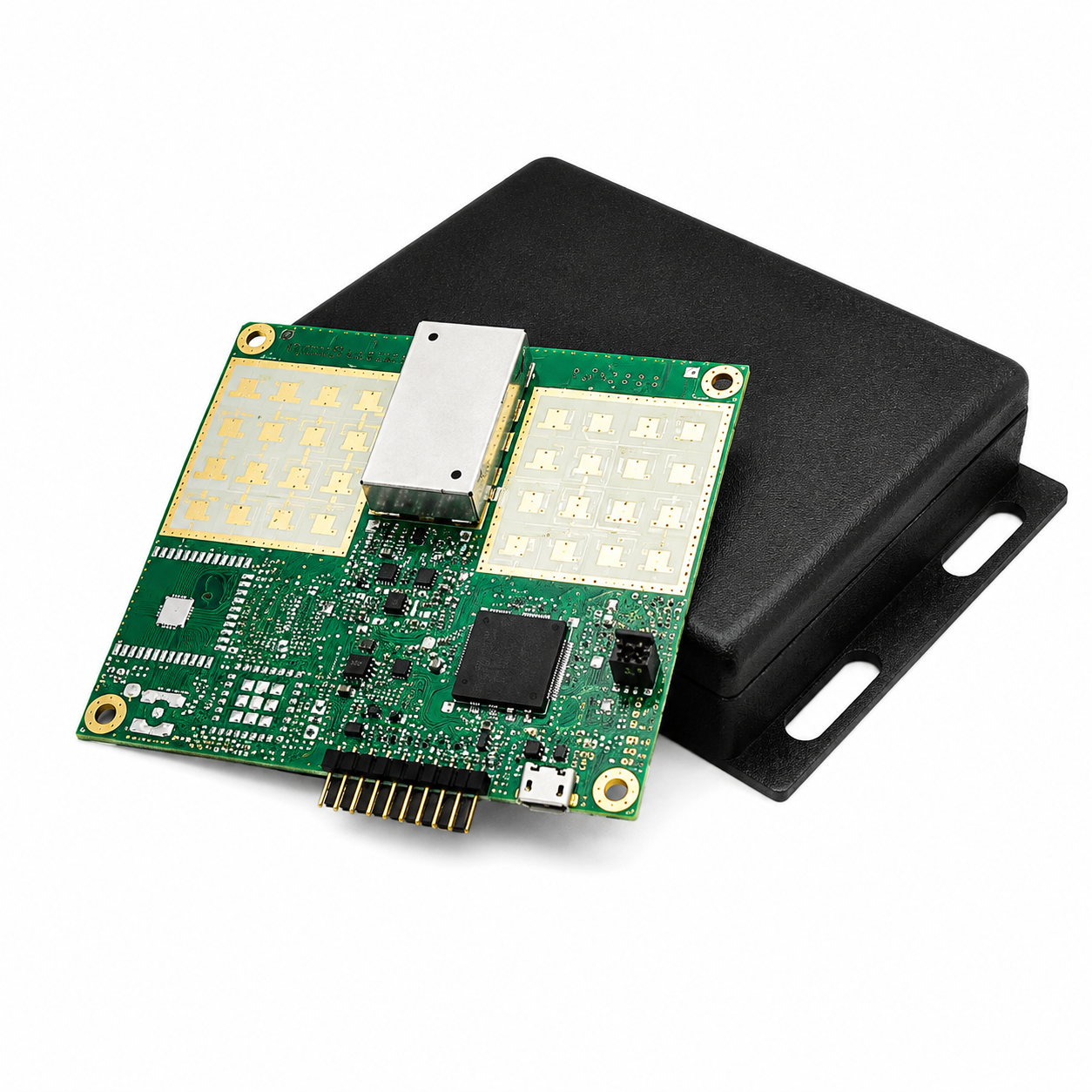
High Frequency PCB Assembly Considerations
Assembly planning matters because RF connectors, shields, modules, fine-pitch components and test access can affect both performance and inspection. A bare board supplier and an assembly supplier should not make separate assumptions about RF areas.
For assembled boards, prepare BOM, CPL, assembly drawing, polarity notes, approved substitutes, RF connector requirements and test procedure. The PCBA service is a useful path when fabrication and assembly need one coordinated review.
Testing and Verification
Testing should be defined before quote approval because not every supplier can verify RF behavior beyond bare-board electrical and impedance checks. If functional or RF performance testing is needed, the buyer may need to provide fixtures, firmware, calibration requirements and pass/fail limits.
| Check | What it verifies | Buyer responsibility |
|---|---|---|
| Electrical test | Open and short conditions | Provide netlist and test scope. |
| Impedance test | Controlled impedance behavior on coupons or traces | Provide target values and tolerances. |
| Assembly inspection | Placement, soldering, polarity and connector quality | Provide BOM, CPL and drawings. |
| RF or functional test | Application-level behavior | Provide fixtures, firmware and acceptance criteria. |
How to Compare High Frequency PCB Suppliers
Compare high frequency PCB suppliers by their questions and assumptions, not only by unit price. A credible supplier should ask about material, stackup, impedance, test method, frequency-sensitive sections and assembly requirements.
- Can the supplier discuss RF materials and hybrid stackups without vague claims?
- Can they review controlled impedance requirements before production?
- Can they state what testing is included and what requires buyer fixtures?
- Can they coordinate fabrication and assembly when connectors or shields matter?
- Do they document quote assumptions instead of hiding uncertainty?
What Determines High Frequency PCB Cost?
High frequency PCB cost depends on RF material, layer count, stackup complexity, impedance control, board size, drilling, finish, testing, quantity and assembly needs. Supplier quotes can vary widely because material and verification assumptions are not always the same.
For broader cost planning, compare the project with the custom PCB cost guide, then ask every supplier to quote the same stackup and test scope.
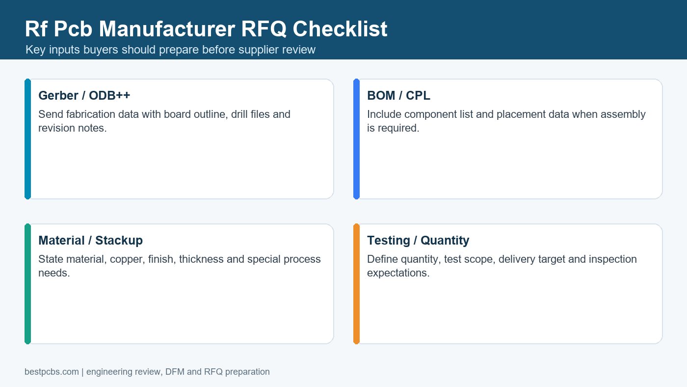
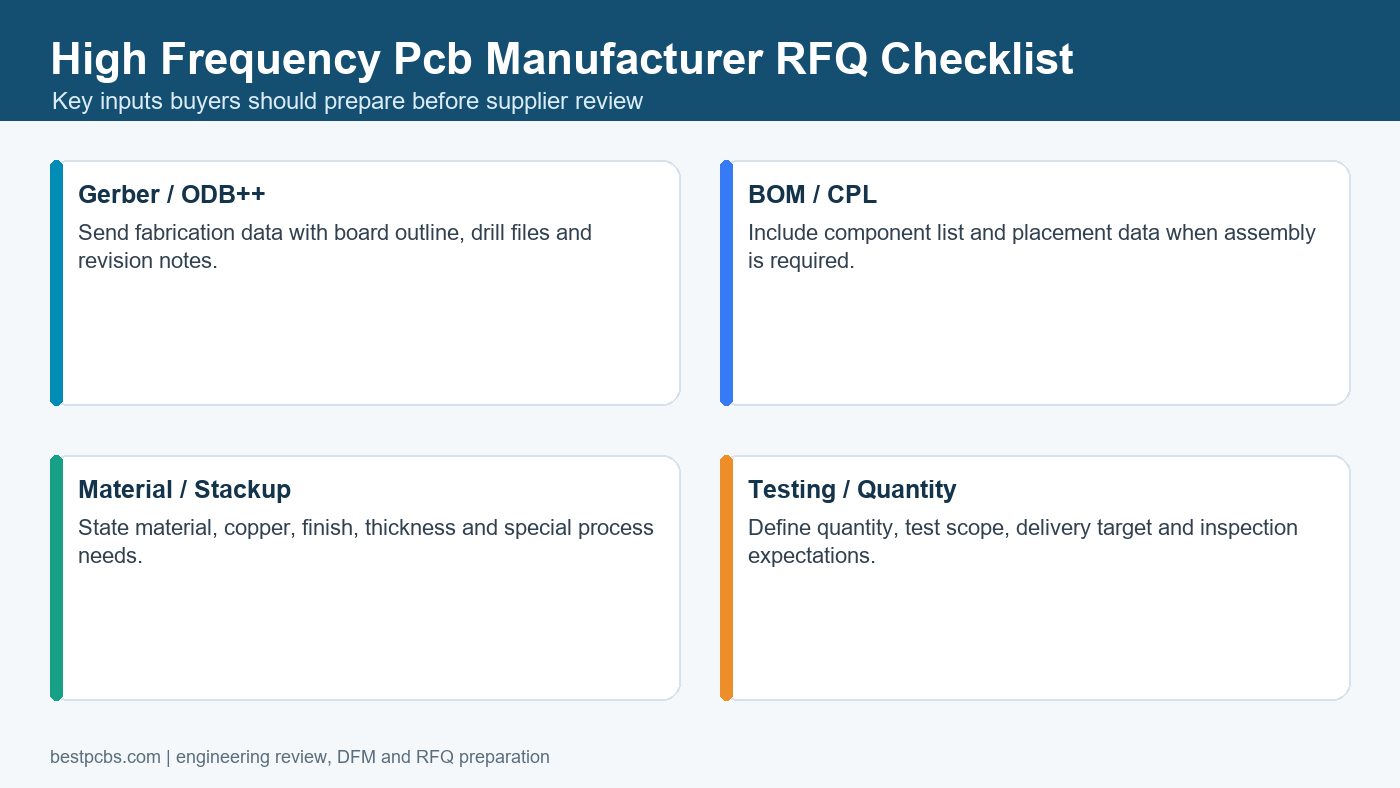
RFQ Checklist for a High Frequency PCB Manufacturer
A strong RFQ should give the manufacturer enough information to quote RF performance risk, not only board size and layer count. Missing material or impedance information can make the first quote unreliable.
- Gerber or ODB++ files, drill files and fabrication drawing.
- Material target, stackup, copper, board thickness and surface finish.
- Controlled impedance values, tolerance and reference plane notes.
- RF areas, connector launches, shields and test requirements.
- BOM, CPL, assembly drawing and polarity notes if PCBA is needed.
- Quantity, target lead time, packaging and delivery destination.
Frequently Asked Questions About High Frequency PCB Manufacturers
Is a high frequency PCB the same as an RF PCB?
The terms often overlap. RF PCB usually refers to radio-frequency behavior, while high frequency PCB can include RF, microwave or high-speed signal applications depending on the project.
Can standard FR-4 be used for high frequency PCBs?
Sometimes, for less demanding sections or lower-risk designs. Higher frequency, lower loss or tighter impedance requirements may need a different material. The material choice should be confirmed by project review.
What should I send to quote a high frequency PCB?
Send Gerber or ODB++, drill files, stackup, material target, impedance requirements, quantity and delivery target. For assembly, also send BOM, CPL and drawings.
What is the biggest sourcing risk?
The biggest risk is accepting a quote that does not define material, impedance, test scope or assembly assumptions. That can create performance or schedule problems after production begins.
Final RFQ Recommendation
Before choosing a high frequency PCB manufacturer, document the RF-sensitive parts of the design and let EBest Circuit review the same files before you commit to a supplier quote. The best decision comes from comparing material assumptions, stackup, impedance, RF layout risk, PCBA scope, testing expectations, cost and delivery planning together.
For a high frequency PCB quote, send your Gerber or ODB++ files, drill data, stackup, material targets, impedance notes, BOM, CPL, assembly drawing, quantity, surface finish, testing requirements and target lead time to sales@bestpcbs.com. EBest Circuit can review the files, flag RF DFM risks, check PCB and PCBA requirements together, and give you a practical quote and production plan for comparison.