PCB manufacturing PCB manufacturing
Home > Blog

Via Stitching: Placement, Spacing, Return Paths, and PCB Design Rules

August 5th, 2026

via stitching is the deliberate use of plated vias to connect copper regions on the same net across PCB layers. It is often applied to ground pours and planes so high-frequency return current can change layers with a signal. The same technique can contain board-edge fields, connect isolated copper to a reference plane, and spread heat through more copper. A useful stitching pattern is driven by current path, frequency, stackup, copper geometry, and fabrication limits—not by filling every open area with holes.

Via stitching test coupon with plated ground vias on a PCB inspection bench

What Is Via Stitching in PCB Design?

Via stitching connects two or more copper areas that belong to one electrical net, usually GND, with repeated plated through holes. A via is itself an interlayer electrical connection; “stitching” describes how multiple vias are placed to make separated copper behave more like one three-dimensional conductor. The term overlaps with via fence, but the design task differs. General stitching distributes connections through pours or planes. A fence places a line or perimeter of vias to constrain fields near a board edge, RF trace, shield boundary, or noisy functional block.

The purpose determines whether a via is useful. A ground via beside a signal transition can shorten the return-current detour. A perimeter row can reduce the length of an electrically open board edge. Vias beneath a grounded thermal pad may also spread heat while bonding ground layers. The same-looking via grid placed far from every relevant current path may deliver little electrical benefit and consume routing area, drill capacity, and inspection effort.

Return via placement beside a signal via changing PCB layers

What Are Stitching Vias Used For?

Stitching vias are used to control return paths, lower interplane connection inductance, contain electromagnetic fields, connect copper pours, support shielding, and sometimes improve heat spreading. These functions are related but not interchangeable, so the drawing should identify the reason for each local pattern.

  • Signal-layer transition: place a ground return via near a signal via when the signal changes reference layers. This lets high-frequency return current follow the transition instead of circulating around a remote plane connection.
  • Ground-pour connection: tie top or bottom copper pours to a solid internal ground plane so the pours do not become floating or weakly connected islands.
  • Board-edge containment: use a via fence along selected edges to reduce parallel-plate and edge-field propagation, especially near connectors, clocks, switching nodes, or RF structures.
  • Functional shielding: surround a sensitive or noisy region with grounded copper and a compatible via fence, while checking openings, connector penetrations, and enclosure bonds.
  • Thermal spreading: create parallel copper paths through the board when the stitched net and land geometry also support heat flow. Thermal-via design still needs its own current, solder-wicking, assembly, and temperature analysis.

How Does Via Stitching Control the Return Current Path?

Via stitching controls return current by providing a nearby connection between the reference conductors used before and after a signal transition. At low frequency, current distribution is influenced mainly by resistance and available copper area. As edge rate increases, return current concentrates near the signal path because the lowest-impedance path is the one that minimizes loop inductance. If the signal changes layers but its reference connection is remote, the return path spreads out, enlarges the loop, and increases coupling and radiation risk.

A return via should therefore be placed according to the signal via and its reference planes, not according to a decorative grid. For a single-ended transition between layers referenced to connected ground planes, one nearby ground via may be the essential connection. For a differential transition, symmetric ground vias can reduce field imbalance, but their location must preserve pair symmetry and avoid narrowing the escape channel.

Texas Instruments interface guidance provides a device-specific example that calls for ground stitching vias symmetrically within 200 mil center-to-center of signal transition vias. This is evidence for that interface context, not a universal rule for every PCB.

If a trace changes from a layer referenced to ground onto a layer referenced to power, a ground via alone cannot directly connect two different nets. The return-transfer method may require a carefully placed decoupling capacitor between the reference planes, a stackup change, or rerouting so the signal retains one reference. Review the complete field path rather than treating “add a via” as a universal cure.

Where and When to Place Stitching Vias?

Place stitching vias where the electromagnetic or thermal path must cross layers. Priority locations include signal transitions, relevant board edges, ground-pour necks, connector returns, shield perimeters, and unavoidable ground discontinuities. Start with the highest-risk current loops and only then fill lower-priority copper regions.

  1. Trace the reference: identify the plane or pour beneath each high-speed segment and note every layer change, split, slot, void, connector, and reference-plane change.
  2. Place transition returns: add the shortest manufacturable ground connection beside each important signal transition. For differential pairs, keep the return structure symmetric.
  3. Close copper bottlenecks: add connections at narrow ground necks and around antipad fields where a pour may otherwise connect through a long path.
  4. Define fence boundaries: place edge or shielding rows only where the field-containment objective, enclosure, and copper geometry support them.
  5. Recheck clearances: confirm antipads do not cut a power or ground plane into a perforated slot, and verify drill-to-copper, hole-to-hole, solder-mask, and component courtyard rules.

Avoid placing vias inside RF transmission structures, antenna keep-outs, creepage paths, flex bend zones, or assembly access areas unless the relevant design rules explicitly allow them. Also inspect via clusters near connectors and BGA escapes; a dense pattern can block routing or weaken the intended plane connection through oversized antipads.

How to Choose Via Stitching Spacing and Fence Pitch?

Via stitching spacing should be calculated from the highest frequency of concern and then checked against stackup geometry, field-containment goals, available copper, and fabrication rules. There is no single pitch that works for every digital, power, RF, or mixed-signal board.

PCB via fence spacing diagram showing repeated ground stitching vias around a guarded region

For a fence intended to suppress propagation, designers often begin with a fraction of wavelength. The wavelength in a PCB structure is shorter than in free space and depends on effective permittivity. A screening calculation can use λ = c/(f√εeff), followed by a conservative fraction such as λ/10 or λ/20.

That result is only a starting ceiling. Transitions, enclosure openings, via diameter, row offset, copper width, and the actual field mode can demand a tighter pattern. The “frequency of concern” must include fast harmonic energy associated with signal rise time, not only the data rate or clock fundamental.

For return vias beside signal transitions, wavelength pitch is not the main decision variable. Minimize the loop and keep the return connection close to the signal via while respecting antipad and routing constraints. For low-frequency copper-pour bonding, use enough vias to avoid long narrow current paths and isolated islands; simulation or impedance measurement may be more useful than a wavelength formula. For thermal or high-current stitching, calculate current sharing and temperature rise separately because current crowding, barrel resistance, copper spreading, and uneven heating prevent ideal equal sharing.

Via Size, Stackup, and Fabrication Rules to Confirm

A stitch pattern is manufacturable only when its hole, pad, annular ring, aspect ratio, drill spacing, copper clearance, and mask treatment fit the selected process. Do not copy a software default without comparing it with the fabricator’s capability table and the project’s reliability class.

Design item What engineering must define What the fabricator must confirm
Finished hole Electrical, thermal, and routing objective Finished-hole tolerance and drill class
Pad and annular ring Required connection and breakout risk Minimum production annular ring after registration tolerance
Board thickness Stackup and via span Allowed through-hole aspect ratio and plating process
Via pitch Return-path or shielding need Minimum hole-to-hole and pad-to-pad spacing
Plane antipad Reference continuity and impedance Etch and registration allowance
Via treatment Open, tented, filled, or capped requirement Compatible fill, mask, planarization, and inspection route

Dense stitching increases drill hits and can add cost or lead time, especially when it introduces a smaller drill class, via fill, sequential lamination, or stricter registration. It can also create unintended copper perforation because every nonconnecting plane needs an antipad around the barrel. Review those voids in every plane layer.

If a pattern sits beneath a component, decide whether tenting or filling is needed to control solder wicking and assembly cleanliness. A procurement package should state the via span, finished hole, pad diameter, treatment, net, and applicable acceptance class rather than relying on appearance alone.

Via Stitching for Differential Pairs and High-Speed Transitions

For differential pairs, stitching vias should preserve a balanced reference transition while limiting return-loop area and discontinuity. Place ground vias symmetrically around the pair where feasible and keep the signal-via geometry matched. Avoid a fence arrangement that forces one conductor to take a different escape path.

Review the transition as a three-dimensional structure. Signal-via barrel length and stubs, pad and antipad dimensions, connector launch, reference-plane separation, and nearby ground vias all influence impedance and mode conversion. Treat impedance control as part of the complete transition, not as a trace-width calculation alone. A pair can remain length matched yet become unbalanced if one signal via sees a different ground-via distance or antipad environment.

At multi-gigabit rates, use the connector or IC vendor layout guide first. Then validate the transition with a field solver, channel simulation, or test coupon when the loss and reflection budget demands it.

Do not place ground vias between the two members of a tightly coupled pair unless the transmission-line design explicitly calls for that topology. The inserted conductor changes coupling and impedance. A via fence alongside a coplanar waveguide is also part of the transmission-line geometry. Include its row offset, pitch, pad diameter, and substrate thickness in the impedance model instead of adding it after routing.

Via Stitching for High-Current and Thermal Paths

High-current and thermal via arrays may look like ground stitching, but they require separate sizing. Use current density, temperature rise, copper spreading, and assembly constraints. Increasing via count reduces the ideal parallel resistance, yet real vias do not share current equally when their approach copper, barrel length, pad geometry, or plane connection differs.

For a power path, calculate the current distribution through the complete copper system: surface trace, neck-down, pads, barrels, internal planes, and exit geometry. Check the hottest corner vias rather than dividing total current by via count. For thermal transfer beneath an exposed pad, evaluate the device datasheet pattern, copper area, board stackup, solder paste aperture, voiding risk, and whether open vias can wick solder. Filled or capped vias can improve assembly behavior but add process steps and must be explicitly specified.

Ground-stitching vias should never bridge nets or defeat an intentional isolation boundary. In safety-spaced regions, a via barrel and its internal-layer pads affect clearance and creepage. In analog layouts, stitching cannot compensate for an uncontrolled common-impedance path. The correct action may be to move the current loop, widen the return, change the stackup, or separate noisy power conversion from a sensitive reference region.

How to Add Stitching Vias in Altium, KiCad, and EasyEDA?

EDA tools can generate stitching arrays, but the operator must first select the correct net, layers, keep-outs, spacing, and via template. Automation accelerates placement; it does not decide whether the pattern supports the real return path.

  • Altium Designer: define a legal via template and select the intended ground net before using the via-stitching or shielding command. Set grid or fence geometry, clearances, and object boundaries, then repour polygons and run the DRC. If Altium cannot add stitching vias or locate an area, confirm that the target polygons are poured and share the selected net. They must also overlap the chosen layers and leave enough room for the via pad plus clearance.
  • KiCad: use the version-appropriate stitching or placement workflow, assign the correct net, and verify that the vias actually connect filled zones on the required layers. Refill zones and inspect connectivity; visually present holes can remain unconnected if a zone excludes them or the net is wrong.
  • EasyEDA: place or array vias with the GND net assigned, then rebuild copper areas and run design-rule and connectivity checks. Confirm exported Gerber and drill files, because a screen view alone does not prove the intended plane connections.

After any automated operation, inspect three outputs: the connectivity report, the plane geometry with antipads, and the fabrication files. Remove orphan vias, vias that land only on isolated copper, and dense groups that block escapes. Lock the approved pattern or document regeneration settings so a later polygon edit does not silently remove its purpose.

How to Verify Via Stitching Before Fabrication?

Verify via stitching with connectivity, geometry, electromagnetic intent, fabrication review, and—when risk justifies it—simulation or measurement. A DRC pass proves only that encoded rules were satisfied; it does not prove the return path is short or the fence suppresses the relevant mode.

  1. Net and layer audit: confirm every stitching via is on the intended net and intersects useful copper on each required layer.
  2. Reference-path audit: trace return continuity through signal transitions, connectors, plane changes, slots, and split boundaries.
  3. Plane-integrity audit: view antipads on all nonconnecting layers and check that via rows do not form a slot or narrow a current path.
  4. Manufacturing audit: compare finished holes, pads, pitch, aspect ratio, mask, fill, and drill classes with the selected process capability.
  5. Fabrication-output audit: inspect Gerber or ODB++ copper, NC drill data, netlist, and a cross-section view before release.
  6. Risk-based validation: use 2D/3D field simulation for sensitive transitions and conduct pre-compliance EMI scans, TDR, VNA, or thermal testing when design margins are limited.

Define pass/fail evidence before testing. For a transition, that may be return loss, insertion loss, mode conversion, or eye margin. Plan EMI/EMC testing in PCBs around the applicable limit, detector, bandwidth, antenna geometry, test method, operating mode, and baseline. For thermal performance, record load, ambient condition, stabilization time, and measurement location. Without these controls, a before/after image or single spectrum peak can mislead.

Common Via Stitching Mistakes and Diagnostic Actions

The most common mistake is treating via count as performance. Diagnose the current path and the failure mechanism before adding more holes.

Observed problem Likely mechanism Next engineering action
EMI changes little after adding a grid Vias are remote from the dominant loop or enclosure opening Locate the source and return path with probing or simulation; move stitching to the coupling boundary
High-speed transition shows excess reflection Signal-via stub, antipad, or reference discontinuity dominates Model the complete transition and adjust stackup, backdrill, pad, antipad, and return vias together
Ground pour remains isolated Wrong net, zone priority, keep-out, or unfilled polygon Repour, run connectivity checks, and inspect exported copper
Plane impedance increases near a via row Antipads perforate or neck down the plane Change pitch, pad stack, row position, or layer routing to restore copper width
Solder is pulled from a thermal pad Open via barrels wick solder Review via fill/cap, tenting, hole size, and paste aperture with the assembler
Fabricator flags drill density or annular ring Pattern exceeds the selected process window Use the approved drill class and spacing or request a documented process exception

FAQs About Via Stitching

Q1: What is the difference between via stitching and a via fence?
A1: Via stitching broadly connects same-net copper across layers. A via fence is a deliberately aligned boundary used for field containment, shielding, or edge control. A fence is one application of stitching, but a general ground grid is not automatically an effective fence.

Q2: Does every signal via need a ground stitching via?
A2: No; prioritize signals whose return current changes reference layers and whose edge rate makes the discontinuity important. Low-speed signals over a continuous reference may not need a dedicated adjacent return via.

Q3: What net should stitching vias use?
A3: Most use GND, but the correct choice is the same net shared by the copper regions being connected. Never stitch different power or ground domains together unless the schematic and isolation plan explicitly requires that connection.

Q4: Can stitching vias cross a split ground plane?
A4: A ground via can only connect copper of the same ground net. It cannot repair a signal crossing between intentionally isolated nets. Reroute the signal or design an approved reference-transfer network.

Q5: Is λ/20 always the correct via spacing?
A5: No; it is only a conservative starting concept for some shielding or fence problems. The relevant frequency, effective permittivity, mode, enclosure, row geometry, and manufacturing constraints determine the final pitch.

Q6: Why is Altium unable to add stitching vias to GND?
A6: Common causes include an unpoured polygon, no overlapping same-net copper on selected layers, a wrong via template or net, and insufficient space after clearance rules. Repour, verify net assignment, and inspect the rule conflict.

Q7: Should stitching vias be tented?
A7: Tenting depends on assembly location, hole size, solder-wicking risk, cleanliness, and fabricator capability. Specify the treatment instead of assuming the solder-mask generator will choose correctly.

Q8: Can stitching vias reduce PCB temperature?
A8: They can improve heat transfer when they connect thermally useful copper, but temperature depends on copper area, barrel geometry, interface resistance, airflow, load, and component package. Validate the complete thermal path.

Q9: Do more stitching vias always reduce EMI?
A9: No; vias help only when they shorten the dominant return path or constrain the relevant field. Poorly positioned vias may add cost, consume routing space, and perforate planes without addressing the emission source.

Q10: What fabrication files should be checked?
A10: Inspect copper layers, NC drill files, netlist, solder mask, fabrication drawing, stackup, and any via-fill or cap notes. Confirm finished hole and pad definitions with the supplier before release.

Conclusion

Effective via stitching begins with a specific job: transfer high-frequency return current, connect useful ground copper, contain an edge field, support a shield, or move heat. Place vias where that path crosses layers, choose pitch from frequency and geometry rather than habit, and verify both the three-dimensional electrical structure and the fabrication outputs. A smaller, well-justified pattern can outperform a dense decorative grid while preserving routing space and process margin.

For a manufacturability review or PCB quotation, send your stackup, Gerber or ODB++ data, NC drill files, netlist, via table, impedance requirements, and via-fill notes to sales@bestpcbs.com. The engineering team can review the proposed stitching geometry against the selected board process.

You may also like

Analog Input vs Digital Input: Which One Fits Your PCB Control System?

July 29th, 2026

Analog input vs digital input comes down to what the controller must learn from a field device. An analog input measures a continuously changing value, such as pressure or temperature. A digital input detects a defined ON/OFF state. Select the channel from the sensor output, required information, timing, noise, diagnostics, and PCB interface.

Analog Input vs Digital Input circuits on a mixed-signal control PCB test bench

Analog Input vs Digital Input: What Is the Main Difference?

An analog input preserves magnitude; a digital input decides between defined states. A 4–20 mA pressure transmitter can report where pressure lies within a calibrated span. A 24 V proximity switch reports whether a target is present, not its distance.

The comparison includes the sensor, cable, connector, protection, filter, isolation, converter or threshold circuit, power, grounding, firmware, and test limits. A pin labeled “analog” or “digital” may still be unsafe for a field signal.

Comparison Dimension Analog Input Digital Input Engineering Impact
Information Magnitude across a range One of two defined states Measurement versus state detection
Common field signals 4–20 mA, 0–10 V, bridge, thermocouple 24 V discrete, dry contact, PNP/NPN, logic level Determines range, loading, and wiring
Receiving hardware Signal conditioning and ADC Threshold detector, buffer, comparator, or optocoupler Changes BOM, area, calibration, and test coverage
Key performance limits Accuracy, resolution, bandwidth, sample rate, drift Thresholds, hysteresis, delay, debounce, switching rate Requires different specifications and tests
Typical failure Noisy, shifted, saturated, or drifting reading False transition, missed state, or indeterminate level Requires different diagnostic paths
Best fit Variable process measurement Events, interlocks, presence, and status Matches the channel to the required information

How Does an Analog Input Measure a Continuous Signal?

An analog input measures a continuous signal through six conversion stages. Each stage must preserve the required range, bandwidth, and accuracy.

  1. Identify the signal. Define the source type, range, impedance, common-mode voltage, return path, cable resistance, and fault voltage. Voltage, current, RTD, thermocouple, and bridge sensors require different front ends.
  2. Protect the connection. Limit ESD, surge, reverse polarity, overvoltage, and fault current. Check protection leakage and capacitance because they can shift high-impedance signals or reduce bandwidth.
  3. Convert and scale. Use a divider or amplifier for voltage, a burden resistor for current, controlled excitation for an RTD, cold-junction compensation for a thermocouple, or an instrumentation amplifier for a bridge. Verify component tolerance, common-mode range, output swing, and power dissipation.
  4. Filter and settle. Set the anti-alias filter from the required bandwidth and response time. For multiplexed ADCs, verify settling after each channel change, especially with high source impedance.
  5. Convert the signal. The ADC produces a code relative to its reference. A 12-bit ADC has 4,096 nominal codes, but offset, gain, nonlinearity, reference drift, noise, grounding, and layout reduce effective accuracy.
  6. Scale and verify. Convert the code into engineering units, build a channel error budget, and test minimum, midpoint, maximum, overrange, settling, and temperature behavior. Averaging reduces random noise but cannot correct clipping or systematic error.

How Does a Digital Input Detect ON/OFF States?

A digital input detects ON/OFF states through six decision stages. The channel must deliver a valid, protected signal to the controller without losing legitimate transitions.

  1. Define the source. Identify PNP, NPN, dry contact, open collector, push-pull, or logic-level output. Document polarity, normally open/closed behavior, logic meaning, and fail-safe state.
  2. Match voltage and current. Compare guaranteed source levels with guaranteed receiver ON/OFF ranges. Include loading and leakage; open-circuit voltage alone does not prove compatibility.
  3. Protect and translate. Add current limiting, polarity protection, transient clamping, level translation, buffering, or isolation. A 3.3 V GPIO is not a protected 24 V industrial input.
  4. Apply thresholds. Use a comparator or Schmitt trigger with adequate hysteresis. Verify threshold margin across supply, temperature, leakage, and ground shift.
  5. Filter invalid transitions. Set hardware filtering or debounce from the shortest valid event. Excess filtering can suppress encoder, flowmeter, or counter pulses.
  6. Capture and verify. Include isolation, comparator, sampling, PLC scan, capture hardware, and software delays. Test minimum HIGH/LOW time and ON, OFF, transition, power-off, and fault states at the controller logic point.

Which Analog Input vs Digital Input Examples Best Explain the Difference?

The clearest examples compare a measured value with a state from the same physical process. A tank may use an analog level transmitter for 0–100% measurement and a digital float switch for a high-level alarm. A motor may use analog current feedback for load trending and a digital overload contact for trip status. A cylinder may use an analog position sensor for travel and digital limit switches for endpoint confirmation.

Application Analog Input Example Digital Input Example Decision Value
Temperature RTD or transmitter value Overtemperature contact Control value versus alarm state
Machine position Linear position sensor Limit switch Travel feedback versus endpoint
Fluid system Pressure or flow transmitter Pressure or flow switch Trend versus interlock
Motor monitoring Current or vibration level Run, fault, or overload contact Condition versus operating state
Operator control Speed potentiometer Start/stop pushbutton Setpoint versus command

Choose by electrical interface and required information. Analog measurement supports control and trending; a switch provides a direct alarm or interlock. Encoders and PWM use digital pulses to encode variable information, while IO-Link, CAN, and RS-485 are digital communication interfaces rather than discrete inputs.

What Hardware Blocks Separate Analog Inputs from Digital Inputs?

An analog path scales and converts magnitude, while a digital path protects and resolves state. The analog chain normally uses protection, a burden resistor or divider, amplification or buffering, an anti-alias filter, optional isolation, an ADC, and a stable reference. Component tolerance, leakage, source impedance, and settling affect the measured value.

A digital path normally uses current limiting, transient and polarity protection, optional isolation, a comparator or Schmitt trigger, and a logic buffer or controller input. Threshold margin, hysteresis, leakage, input current, delay, and minimum pulse width determine whether the state is dependable.

  • Analog interface definition: signal range, common-mode range, source impedance, return path, shield connection, cable resistance, and differential or single-ended behavior.
  • Digital interface definition: ON/OFF voltage and current, PNP/NPN or dry-contact behavior, wetting current, pulse width, debounce, and fail-safe state.
  • Shared checks: connector pinout, fault voltage, surge environment, isolation boundary, field ground, and power dissipation.

Isolation can appear in either chain, but its implementation differs. An isolated analog channel may use an isolation amplifier, isolated ADC, or converter plus digital isolator and isolated power. An isolated digital channel may use an optocoupler, digital isolator, isolated comparator, or relay interface. The isolation component alone is insufficient: the PCB must maintain the required separation, and any shield, test point, copper pour, mounting hardware, or power converter crossing the boundary must be reviewed.

Mixed-signal control PCB with separate analog front-end and isolated digital input component regions

How Do 4–20mA and 0–10V Analog Inputs Compare with 24V Digital Inputs?

4–20 mA and 0–10 V carry proportional measurements; a 24 V digital input carries a state. A current loop tolerates cable resistance provided that the loop has sufficient compliance voltage. A voltage input depends more directly on reference differences, loading, leakage, and voltage drop. A discrete input depends on valid ON/OFF current and voltage margins.

Comparison Dimension 4–20 mA Analog 0–10 V Analog 24 V Digital Selection Check
Information Proportional measurement Proportional measurement ON/OFF state Magnitude or state?
Receiver Burden resistor and ADC path Divider/buffer and ADC path Limiter and threshold/isolation path Range, impedance, and dissipation
Wiring sensitivity Loop compliance limits series drop Reference and loading affect voltage Threshold margin dominates Cable, returns, and grounding
Diagnostics Live zero may identify some faults 0 V may be valid or faulty OFF may be valid or faulty Define detectable failures
Typical use Industrial transmitters Local controls and instrumentation Switches and interlocks Match the field-device data sheet

For 4–20 mA, verify the loop voltage budget before choosing the burden resistor. The supply must cover the transmitter’s minimum operating voltage, cable and barrier drop, receiver drop, and other series elements at the highest expected current. A 250 Ω burden produces 1–5 V at 4–20 mA and dissipates 0.1 W at 20 mA, but component rating must also consider overrange and fault conditions. The value is an example, not a universal requirement.

For 0–10 V, verify the reference-to-ground difference, input impedance, common-mode range, rail linearity, shielding, and possible negative voltage. For 24 V digital inputs, verify guaranteed ON/OFF regions, source type, leakage, input current, hysteresis, and voltage drop across the protection circuit. A general-purpose PLC input is not automatically safety-rated.

How Do Analog Input Resolution and Sampling Rate Compare with Digital Input Switching Speed?

For analog input vs digital input performance, resolution and sampling rate describe analog measurement, while switching speed describes digital state detection. They are not interchangeable specifications and must be verified with different stimuli.

Comparison Dimension Analog Resolution Analog Sampling Rate Digital Switching Speed Design and Verification
Primary purpose Defines the smallest nominal code step Defines how often conversions occur Defines how fast transitions can be recognized Start from required measurement change or event timing
Key calculation Ideal code size = VFS/2N Per-channel rate depends on ADC rate, channel count, and settling Maximum rate depends on minimum HIGH/LOW time and total delay Calculate the complete channel, not one component rating
Practical example 0–10 V at 12 bits gives about 2.44 mV per nominal code A multiplexed ADC may provide less usable rate per channel A filtered 24 V input may reject a valid short pulse Use actual range, filtering, topology, and controller timing
What it does not prove Resolution does not prove accuracy or noise-free bits Sample rate does not equal usable signal bandwidth Fast device delay does not prove system event capture Check sensor, front end, reference, filter, scan, and software
Main error or loss Noise, offset, gain, reference error, drift, or clipping Aliasing, incomplete settling, or channel-to-channel memory Missed pulses, chatter, excessive latency, or indeterminate states Test minimum, maximum, boundary, and dynamic conditions
Filter trade-off Lower noise can improve stable readings Narrower bandwidth increases response and settling time Longer debounce rejects noise but reduces event rate Preserve the fastest valid signal or pulse
Selection rule Choose bits from meaningful change and the total error budget Choose rate from bandwidth, channels, acquisition, and latency Choose speed from pulse width, delay, filtering, capture, and scan time The slowest stage sets usable system performance
Verification method Inject calibrated increments and measure noise-free response Apply timed steps and verify settling on every channel Apply worst-case pulse trains at minimum valid amplitude Test at supply and temperature limits with real firmware timing

Why Do Analog Input vs Digital Input Circuits Respond Differently to Noise and Interference?

In analog input vs digital input circuits, noise changes the analog reading directly but affects the digital result mainly when it crosses a threshold or corrupts timing. Digital inputs still fail when interference crosses a threshold, ground shift moves the signal outside its valid range, or filtering removes a legitimate short pulse.

Analog interference appears as variation, offset, ripple, or saturation; narrow bandwidth reduces noise but increases settling time. Digital inputs tolerate disturbances inside their noise margin, but slow edges, insufficient hysteresis, ground shift, or threshold-crossing transients can cause chatter or false states.

  • Connector disturbance: Quantify the normal signal and credible interference at the connector.
  • Digital margin: Verify threshold margin across supply, temperature, leakage, and ground shift.
  • Analog bandwidth: Set bandwidth from the required response, then measure settling.
  • PCB separation: Keep relays, converters, clocks, gate-drive loops, and high-current traces away from sensitive analog paths.
  • Immunity validation: Test immunity to ESD, burst, surge, cable transients, and common-mode disturbances against the end-product requirements.

What Signal Conditioning and Protection Does Each Input Type Require?

Analog conditioning must preserve magnitude, while digital conditioning must preserve state and timing. Select the divider or burden resistor for range and dissipation, keep amplifier common-mode and output swing within limits, set filter cutoff from signal bandwidth and ADC settling, and include reference and tolerance errors in the budget. Protection leakage and capacitance must not corrupt the source.

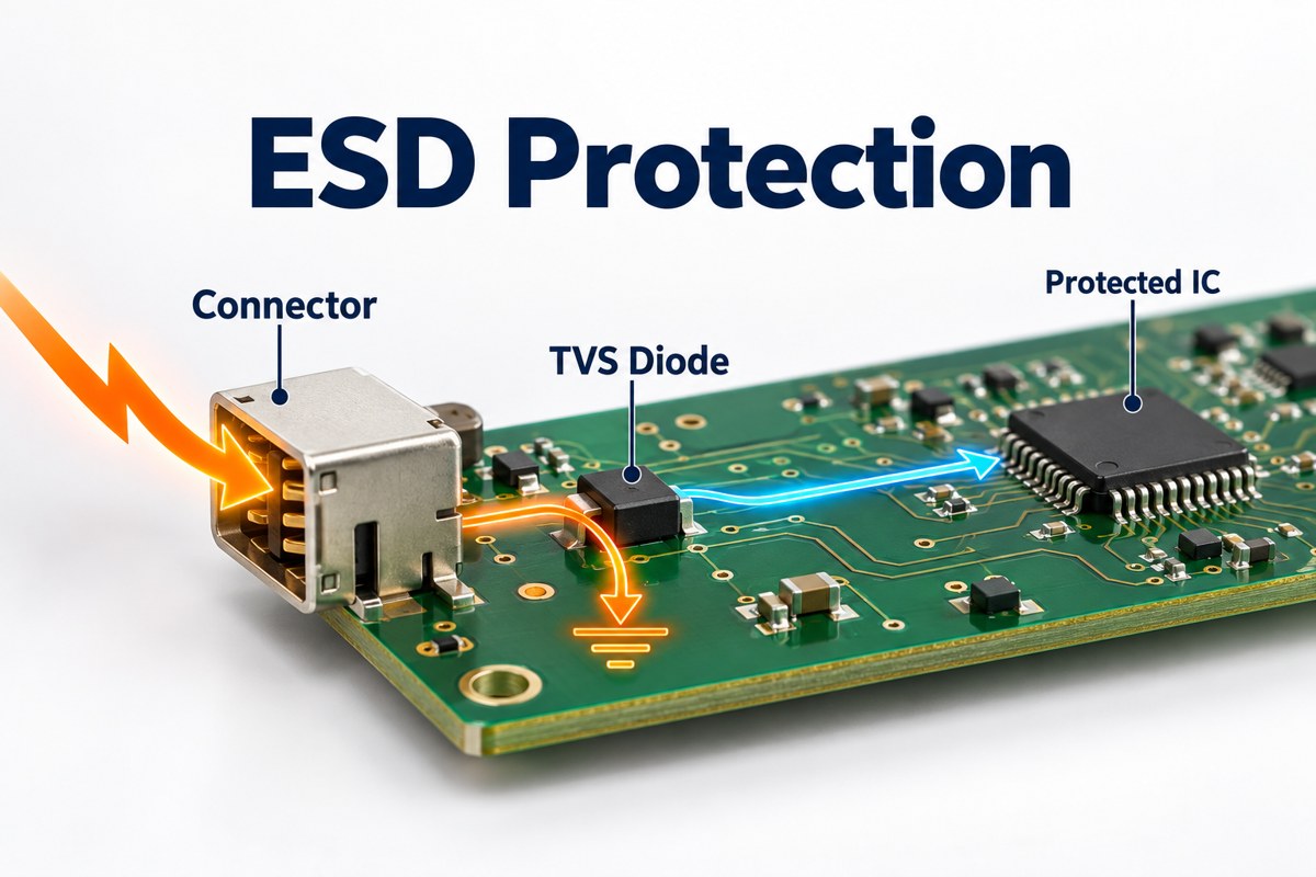
Protection must survive the fault without invalidating normal measurements or states. A TVS diode must be coordinated with series impedance and downstream absolute maximum ratings; its dynamic clamp voltage, leakage, and capacitance matter. A resistor must be checked for working voltage, pulse energy, temperature rise, and fault dissipation, not only nominal resistance. Where sustained overvoltage is credible, a fuse, resettable protector, current limiter, or disconnect device may be necessary.

  1. Define normal and fault ranges. Include source impedance, cable, grounding, and power-off states.
  2. Select protection. Coordinate current limiting, clamps, TVS devices, fuses, and isolation with the available fault energy.
  3. Set the analog transfer path. Calculate scaling, gain, bandwidth, settling, and error contribution.
  4. Set the digital decision path. Calculate ON/OFF current, thresholds, hysteresis, delay, and minimum pulse width.
  5. Verify at temperature and supply limits. Nominal bench behavior does not prove boundary margin.

How Are Analog and Digital Inputs Used in PLC Systems?

A PLC digital module reports states, while an analog module reports scaled measurements. The digital input evaluates field voltage or current against ON/OFF thresholds and places the state in process data. Input filtering can suppress bounce and short noise pulses, but it adds delay. High-speed counters require channels specified for the pulse frequency and minimum HIGH/LOW time.

Match the module to two-, three-, or four-wire transmitters; PNP or NPN sensors; shared or isolated returns; and required wire-break or overrange diagnostics. Check isolation, input impedance, update time, accuracy over temperature, terminal wiring, and fuse requirements in the module data sheet.

PLC configuration must match the physical module and field wiring. For an analog channel, select current or voltage mode, engineering-unit scaling, filtering, update behavior, and diagnostic limits. If a 4–20 mA transmitter is scaled as 0–20 mA, the value and fault interpretation will be wrong even when the wiring is correct. For a digital channel, confirm input polarity, filtering time, normally open or normally closed logic, and whether the application needs a standard, interrupt, counter, or safety input.

At commissioning, compare the terminal signal, raw module value, and scaled PLC tag. This separates field, module, and program faults. Review individual, group, or backplane isolation before combining commons; software forcing does not verify field wiring or protection.

How Should You Choose Between Analog and Digital Sensor Inputs for Automation?

Choose the required information first: measurement, state, event, or a combination. Then match the receiving channel to the sensor’s electrical output and to normal, boundary, and fault conditions. This keeps the choice between analog and digital sensor inputs tied to the control task rather than the connector label.

  1. Define the control task. Specify the range, alarm, event, or interlock.
  2. Read the sensor output specification. Identify 4–20 mA, 0–10 V, bridge, thermocouple, dry contact, PNP, NPN, open collector, or logic level.
  3. Match electrical limits. Check voltage, current, impedance, common-mode range, leakage, thresholds, and fault exposure.
  4. Set performance. Define analog accuracy, bandwidth, sample rate, and drift or digital delay, pulse width, debounce, and switching rate.
  5. Assess installation conditions. Include cable length, shielding, grounding, nearby switching, temperature, moisture, and isolation.
  6. Define diagnostics. Decide how the system distinguishes a valid minimum or OFF state from open wire, short circuit, or lost sensor power.
  7. Verify the complete channel. Test the sensor, cable, PCB, scaling or logic, and fault response together.

Prefer analog when control quality depends on how much; prefer digital when the decision depends only on whether. A proportional valve controller needs position or pressure magnitude, while an emergency stop, guard switch, or end limit needs an unambiguous state. If the process needs an alarm threshold that may change in software, an analog measurement provides flexibility. If the threshold must remain independent of the controller, a separate switch can provide a distinct hardware signal.

For procurement, specify the signal standard, range, sourcing or sinking behavior, supply, pinout, isolation, cable, environment, accuracy or timing, and fault diagnostics. Analog channels may add calibration and shielding costs; several digital switches may be needed to represent multiple operating points.

How Should Mixed Analog and Digital Input Data Acquisition Hardware Be Designed on a PCB?

Design mixed-input PCBs from voltage domains, current paths, timing, and fault containment. The hardware must protect field connections without allowing switching current, ground shift, or shared conversion resources to corrupt analog results or digital events.

  1. List channel roles and domains. Identify measurements, states, triggers, interlocks, field power, chassis, isolated supplies, analog ground, and digital ground.
  2. Place protection at each connector. Keep ESD, surge, polarity, and current-limiting components near the entry point.
  3. Keep input chains compact. Group analog scaling, amplification, filtering, reference, and ADC components; group digital protection, isolation, threshold, and buffer components.
  4. Control return currents. Maintain a continuous reference where appropriate and prevent fast digital returns from crossing sensitive analog paths.
  5. Allocate conversion and timing resources. Account for ADC multiplexing, per-channel settling, digital timestamp needs, shared clocks, processor load, and simultaneous operation.
  6. Separate noisy nodes. Increase distance from relays, switching regulators, gate-drive loops, clocks, memory buses, and high-current traces.
  7. Implement real isolation boundaries. Check creepage, clearance, slots, copper keepouts, component ratings, and isolated power against working voltage and applicable safety conditions.
  8. Provide diagnostics and test access. Include safe test points, range status, wire-break or overrange handling, calibration storage, and production-test access.
  9. Review before release. Verify connector pinout, fault paths, shields, return paths, isolation-domain labels, and simultaneous analog/digital operation.

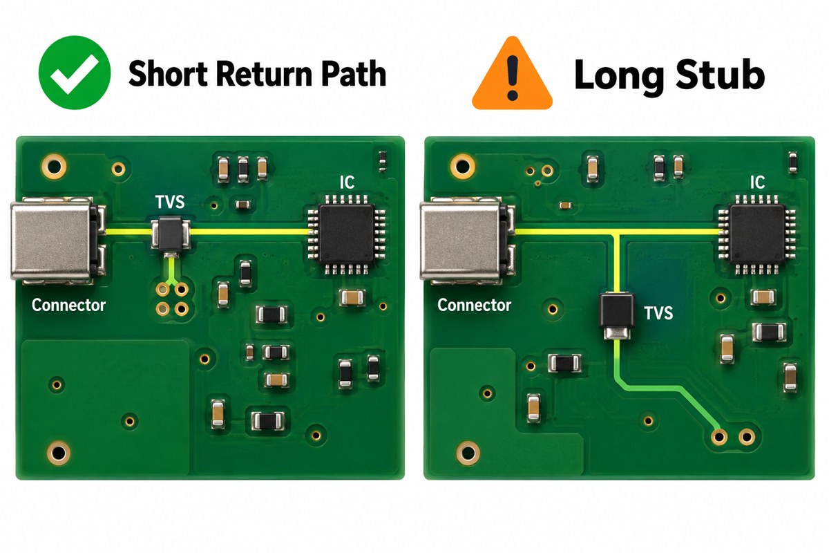
Partition placement by current flow and fault energy, not by labels alone. Put connector protection first, then scaling or current limiting, isolation where required, and finally sensitive conversion or logic. Keep a short, low-inductance return for transient clamps to the intended chassis or reference node. Do not route surge current through the analog ground used by the ADC reference.

Review analog and digital tolerances as channel-level stacks, including scaling, offset, reference, thresholds, leakage, delay, and fault dissipation. Keep test points on the correct side of each isolation barrier and define how production fixtures stimulate, identify, calibrate, and record every channel.

How Can Analog Input vs Digital Input Circuits Be Tested, Calibrated and Troubleshot?

Analog input vs digital input testing must cover boundaries and faults, not only nominal operation. Use calibrated sources and define acceptance limits before testing.

  1. Inspect the unpowered assembly. Verify polarity, values, spacing, connector mapping, solder quality, shorts, and resistance to ground.
  2. Power each domain with current limiting. Check rails, references, isolated supplies, and unexpected heating.
  3. Test digital thresholds and timing. Sweep rising and falling levels; verify hysteresis, OFF leakage, ON current, minimum pulse width, debounce, and fail-safe state.
  4. Test analog endpoints and midpoints. Inject calibrated minimum, midpoint, and maximum values; check offset, gain, linearity, saturation, and channel consistency.
  5. Calibrate where required. Calculate coefficients from traceable stimuli, store them with channel identity and revision, and verify the corrected result independently.
  6. Measure dynamic response. Apply analog steps and digital pulses; record settling, latency, missed events, and filter effects.
  7. Inject credible faults. Test open wire, safe shorts, reversal, overrange, and loss of field power.
  8. Evaluate interference. Operate nearby relays, motors, converters, and communications while monitoring readings and transitions.
  9. Correlate hardware and software. Compare connector signal, conditioned node, ADC code or logic state, scaling, alarms, and displayed value.
  10. Define production limits. Convert results into fixture stimuli, pass/fail windows, calibration records, and traceable functional tests.
Engineer testing analog and digital input channels on a mixed-signal PCB at a validation bench

Trace the signal stage by stage instead of replacing components by guesswork. Disconnect or simulate the field source, inject a known value at the connector, and follow it through each accessible node. If the conditioned voltage is correct but the reported value is wrong, investigate the ADC reference, channel selection, calibration, and scaling. If the connector signal is correct but the conditioned node is wrong, check for damaged protection components, incorrect component values, leakage, loading, common-mode violations, or solder defects.

Capture intermittent digital faults at the field and receiver nodes to check bounce, ringing, thresholds, delay, and pulse width. For analog drift, log sensor output, reference, supply, temperature, and converted data. Set production limits from design tolerance and measurement uncertainty, then record revision, stimulus, calibration, result, and status.

What Are the Most Common Questions About Analog Input vs Digital Input?

Q1: Can one universal input channel accept both analog and digital sensors?

A1: Yes, but only when hardware provides selectable protection, range, analog-conversion, and digital-threshold paths. Firmware selection cannot make one fixed front end safe for every source. Treat it as multiple validated electrical modes.

Q2: What happens if 24 V is connected directly to an MCU input?

A2: A typical low-voltage MCU pin can be overstressed or destroyed. Use current limiting, clamping, level translation, or isolation designed for the fault voltage, duration, and source impedance.

Q3: Is a pulse or frequency signal a digital input?

A3: Usually, because the receiver counts threshold crossings. Check frequency, minimum HIGH/LOW time, delay, and counter capability before using a high-speed digital or counter channel.

Q4: How should unused inputs be terminated?

A4: Do not leave a high-impedance input floating. Apply the receiver’s recommended bias or termination and configure a defined, safe, and detectable state.

Q5: Can analog and digital inputs share one connector?

A5: Yes, after reviewing pin assignment, spacing, returns, shielding, and miswiring. Use a keyed, documented pinout and protect an analog pin from credible digital-supply faults.

Q6: Is an I2C, SPI, CAN, or RS-485 sensor a digital input?

A6: It provides digital data but is not a discrete ON/OFF input. It needs protocol handling and the correct logic interface or transceiver. Classify it as a digital communication interface.

Q7: What should an input do when the controller is powered off?

A7: The field source must not back-power an unpowered controller through protection diodes or interface components. Check current paths for every power sequence and use suitable blocking, limiting, buffering, or isolation so the channel enters a defined power-off state.

Q8: Can one sensor provide both an analog value and a digital alarm?

A8: Yes. Some sensors provide a proportional output plus a configurable switch output. Treat them as two electrical interfaces: verify each output type, reference, loading, timing, and fault behavior before connecting them to separate compatible input channels.

Q9: When is a ratiometric analog measurement useful?

A9: Ratiometric conversion is useful when the sensor output and ADC reference change with the same excitation voltage. The shared variation can cancel in the calculated ratio, provided the excitation and reference remain properly related and within their operating ranges.

Q10: How can input impedance be checked without disturbing the circuit?

A10: Measure the voltage change produced by a known source resistance or apply a small, controlled test signal within safe limits. Include instrument loading and protection leakage in the calculation; use a buffered method when the source is too sensitive for direct probing.

Send your schematic, Gerber files, BOM, input ranges, channel count, isolation requirements, operating environment, and test criteria to EBest Circuit at sales@bestpcbs.com for a PCB and PCBA quotation.

You may also like

How It Works Grounding Bus: PCB Return Paths and Layout Rules

July 24th, 2026

The phrase how it works grounding bus usually refers to how a shared conductor provides a common reference and return-current path. In a PCB, the grounding bus may be a wide copper trace, copper region, or connection to a ground plane. Its effectiveness depends on impedance, geometry, frequency, and where each current enters and leaves the shared path.

How a PCB grounding bus works as a low impedance return path

What Is a PCB Grounding Bus?

A PCB grounding bus is a shared copper conductor used to connect multiple circuit returns to a common ground node. At DC it carries return current with a voltage drop determined mainly by resistance. At higher frequency, inductance and current-loop geometry can dominate, so a conductor that looks wide enough for DC may still create noise.

The term should not be confused with the ground bar in a building service panel. A PCB ground bus belongs to the electronic signal and power-return structure; its design is governed by circuit current paths, signal bandwidth, isolation, EMC, and board construction.

How Does a PCB Ground Bus Work?

Current always returns to its source. A grounding bus gives several circuit branches a shared route back to the supply, converter, driver, or signal source. If the bus impedance were zero, all connection points would remain at the same potential. Real copper has resistance and inductance, so current from one branch can create a voltage difference seen by another branch.

The resulting error is approximately the return current multiplied by the relevant impedance. Slow, low-current circuits may tolerate a shared trace. Fast switching or high-current circuits can create ground bounce, common-impedance coupling, timing errors, ADC offset, audio hum, or radiated emissions.

PCB ground bus showing shared return current and voltage drop

Why Must Ground Impedance Stay Low?

Ground is a reference node, not a perfect physical zero. A return path with resistance R and inductance L develops both an IR drop and an L × di/dt voltage. The inductive term becomes important when current changes rapidly, even if the average current is small.

For example, a switching edge with high di/dt can create hundreds of millivolts across a short inductive return path. That disturbance may be comparable with the noise margin of a logic interface or several least-significant bits of a precision converter. Low impedance therefore requires more than sufficient copper cross-section; it requires a short, continuous path with a small loop area.

Ground Bus vs Ground Plane vs Star Ground

Structure Current path Best use Main limitation
Ground bus trace Current follows a defined shared conductor Low-frequency, controlled branch returns, single-layer constraints Common impedance and trace inductance
Ground plane Return current uses a broad continuous copper layer High-speed, mixed-signal, multilayer and EMC-sensitive boards Slots and splits can interrupt the path
Star ground Branches meet at one selected node Separating noisy power returns from sensitive analog returns Poor physical placement can create long loops

A modern multilayer board normally uses a continuous circuit board ground plane for high-frequency return current. A bus or star point may still be useful for controlling how high current, chassis current, or low-frequency analog current joins that plane.

When Should a PCB Use a Ground Bus?

A defined ground bus can work in low-frequency power distribution, simple analog circuits, single-sided prototypes, LED drivers, relay controls, and boards where branch currents need an intentional connection order. It can also connect several local copper regions to a selected star point.

It is a weak choice when fast signals cross the board, switching currents share the same narrow return, or connectors create several remote ground entry points. In those cases, a plane or wider copper region generally provides lower impedance and a more predictable return path.

How Should Analog, Digital and Power Grounds Connect?

Start by tracing current loops rather than assigning ground names alone. Keep high-current switching loops local to their power stage. Give precision analog inputs a quiet reference path. Place decoupling capacitors so their return current closes directly to the relevant IC ground and plane.

Analog and digital regions may share one solid plane when placement keeps noisy currents away from sensitive paths. If separate regions are required, connect them at a deliberate point that matches the converter or isolation architecture. Do not route a high-speed signal across a ground split, because its return current must detour around the gap.

Analog digital and power ground return paths on a PCB

How Do Current and Frequency Change the Layout?

DC voltage drop depends on copper resistivity, length, width, and thickness. Higher current may require wider traces, heavier copper, multiple vias, or a busbar connection. At high frequency, return current concentrates near the signal path because that geometry minimizes loop inductance.

Rise time is often more important than nominal clock frequency. A low-frequency signal with a fast edge can still require a continuous reference plane. Connector pinout, via transitions, plane changes, cable shields, and chassis bonds must be included in the complete loop.

What Grounding Bus Mistakes Cause Noise and EMI?

  • Routing sensitive analog return current through a high-current switching segment.
  • Using a long narrow ground trace for MOSFET, relay, motor, or converter pulse current.
  • Splitting a ground plane beneath a high-speed signal.
  • Connecting local grounds at several uncontrolled points and creating a PCB ground loop.
  • Placing decoupling capacitors far from the power and ground pins they serve.
  • Using too few vias between ground regions or layers.
  • Treating chassis, protective earth, shield, analog ground, and power return as interchangeable nodes.

Correcting the schematic symbol without changing the physical return path will not solve these problems. Grounding performance is determined by copper geometry and current flow on the finished board.

How Can a Ground Bus Be Checked on a Prototype?

Measure DC voltage drop along the bus under representative load, then observe noise between selected ground points with a short ground spring or differential probe. A long oscilloscope ground lead can add enough loop inductance to create a misleading waveform.

Test the board during worst-case switching, load steps, communication activity, and cable connection. Near-field scanning, conducted-emissions tests, thermal imaging, and current probes can reveal return paths that are not obvious from the schematic.

PCB ground bus prototype testing with differential probing

How Does PCB Construction Support a Low-Impedance Ground?

Layer stack-up should place critical signal layers next to a continuous reference plane. Copper thickness, via count, drill size, plane clearance, isolation requirements, and solder-mask openings affect the manufactured return structure. A 2 layer PCB ground plane needs careful component placement and routing to preserve copper continuity.

EBest Circuit (Best Technology) supports multilayer PCB fabrication, controlled stack-ups, impedance control, heavy copper, via structures, and PCB assembly. Engineering review can identify plane splits, insufficient copper connections, manufacturability conflicts, and assembly features that would alter the intended current path.

FAQ About PCB Grounding Buses

How exactly does grounding work on a PCB?

Grounding provides a reference potential and closes current loops back to their sources. It does not make current disappear; it controls where return current flows and how much unwanted voltage develops along that path.

Is a ground bus the same as a ground plane?

No. A bus is usually a defined shared conductor, while a plane is a broad copper layer or region. A plane normally provides lower high-frequency impedance, but both can be part of one grounding system.

Can ground and neutral be on the same bus bar?

That question normally concerns building service panels, not PCB layout. Neutral and protective-earth bonding must follow the applicable electrical code and installation point; it should not be inferred from PCB grounding rules.

Should analog and digital ground always be split?

No. A solid plane with controlled placement and return paths is often better. Split grounds are justified only when the architecture and current paths require them, and signals must not cross the split without an intentional return path.

How many ground vias should be used?

The answer depends on current, frequency, layer transition, via geometry, and EMI requirements. Use enough vias to avoid creating a narrow inductive neck, and place them close to the current transition rather than far away.

Conclusion

How it works grounding bus becomes clear when the design is treated as a current-return problem. A useful PCB ground bus provides a short, low-impedance shared path without allowing noisy branch currents to disturb sensitive references. At higher frequency, a continuous ground plane and controlled loop geometry usually outperform a narrow shared trace.

For PCB stack-up, grounding, fabrication, or assembly support, contact EBest Circuit (Best Technology) at sales@bestpcbs.com.

You may also like

Intercom Circuit Board Design, Manufacturing and Assembly Services for Wired and Wireless Systems

July 10th, 2026

An intercom circuit board integrates voice capture, audio processing, wired or wireless communication, power management and access-control functions. Reliable operation depends on circuit architecture, PCB layout, component quality, firmware and production testing. EBest Circuit provides custom PCB manufacturing and assembly services for door-entry systems, wireless intercoms, building communication panels and industrial talkback equipment.

Are you worried about these problems in intercom circuit board projects?

  • Design challenges: Poor grounding, incorrect gain settings or unsuitable antenna placement may cause noise, echo, weak audio and unstable wireless communication.
  • Production risks: Incomplete files, material shortages and uncontrolled impedance may delay prototypes or affect batch consistency.
  • Assembly difficulties: Fine-pitch parts, microphones, wireless modules and hidden solder joints require precise placement and reliable inspection.

As a one-stop PCBA service provider with more than 20 years of industry experience, EBest Circuit provides the following solutions:

  • Design optimization: We review audio circuits, power distribution, grounding, RF routing and antenna layout to reduce noise and communication failures.
  • Controlled production: We verify manufacturing files, materials, impedance and component availability before fabrication to reduce delays and redesigns.
  • Reliable assembly and testing: We provide SMT and THT assembly, SPI, AOI, X-ray, programming and functional testing to verify product performance.

Send your Gerber files, BOM and test requirements to EBest Circuit via sales@bestpcbs.com for a quotation.

Intercom Circuit Board, https://www.bestpcbs.com/blog/2026/07/intercom-circuit-board/

What Is an Intercom Circuit Board?

An intercom circuit board is the electronic platform that receives, processes, transmits and reproduces voice and control signals between communication stations. It is used in analog door-entry units, digital building systems, wireless handsets, IP intercoms and industrial communication terminals.

The board connects microphones, speakers, call buttons, displays, relays, power inputs and communication interfaces. A basic intercom PCB may use analog amplifiers and switching circuits, while an advanced design can include an MCU, DSP, audio codec, wireless module, Ethernet PHY and access-control output.

The circuit architecture depends on audio quality, communication distance, network type, enclosure size, power source and operating environment.

What Functions Does an Intercom PCB Control?

An intercom PCB controls audio capture, signal processing, communication, user commands and power distribution. The exact functions depend on whether the product is analog, digital, wired, wireless or IP-based.

Common functions include:

  • Capturing voice through an electret or MEMS microphone
  • Filtering and amplifying microphone signals
  • Converting audio between analog and digital formats
  • Driving speakers, handsets or headsets
  • Supporting half-duplex or full-duplex communication
  • Processing buttons, keypads and status indicators
  • Controlling electric locks, relays and alarms
  • Managing WiFi, Bluetooth, RF, Ethernet or two-wire connections
  • Regulating input power into separate voltage rails
  • Storing firmware, addresses and operating settings
  • Protecting external interfaces against ESD and voltage surges

Stable performance requires these functions to operate without introducing noise, distortion or communication interference.

What Are the Main Components of an Intercom Circuit Board?

An intercom circuit board normally includes audio input, signal processing, communication, speaker output, power and protection circuits. The actual configuration depends on the system architecture and product functions.

ComponentTypical SelectionMain Function
MicrophoneElectret, analog MEMS or digital MEMSCaptures voice
Microphone front endBias circuit, low-noise amplifier and filterConditions weak microphone signals
Audio codecADC, DAC and I²S interfaceConverts analog and digital audio
ProcessorMCU, DSP or application SoCControls audio, communication and system logic
Program memorySPI NOR, EEPROM, NAND or eMMCStores firmware and configuration
Working memoryInternal SRAM or external DDRBuffers audio and processing data
Audio amplifierClass AB or Class DDrives the speaker or handset
Speaker interfaceFilter, protection and connectorConnects and protects the speaker output
Wireless circuitSub-GHz, Bluetooth or WiFi moduleProvides wireless communication
RF networkMatching components, RF feed and antennaTransfers RF energy to the antenna
Wired interfaceTwo-wire line interface or RS-485 transceiverSupports wired communication
Ethernet interfacePHY, magnetics and RJ45 connectorSupports IP communication
PoE circuitPoE PD controller and DC-DC converterReceives power through Ethernet
Access-control outputRelay, MOSFET or transistor driverControls locks, alarms or gates
User interfaceButtons, keypad, LEDs or display driverProcesses commands and status
Clock and resetCrystal, oscillator and reset ICControls timing and startup
Power supplyBuck, boost or LDO regulatorGenerates stable voltage rails
Protection circuitFuse, TVS, ESD and reverse-polarity protectionProtects power and external interfaces
Debug interfaceSWD, JTAG, UART or USBSupports programming and diagnostics
ConnectorTerminal block, FFC or board-to-board connectorConnects external devices

A basic analog board may not require a processor, external memory or Ethernet circuit. An IP intercom with video, networking or an operating system may require a higher-performance SoC, DDR and eMMC.

The microphone front end, power supply, grounding, speaker amplifier and communication interface have the greatest influence on audio clarity and stability.

Intercom Circuit Board Components, https://www.bestpcbs.com/blog/2026/07/intercom-circuit-board/

How to Read an Intercom Circuit Board Schematic and Block Diagram?

Read the functional block diagram first to understand the complete signal flow. Then use the schematic to verify how each circuit is powered, controlled and connected.

  • Identify the system type: Confirm whether the product is analog, digital, two-wire, wireless or IP-based.
  • Trace the power tree: Follow the input through the fuse, reverse-polarity protection, surge protection and voltage converters.
  • Follow the microphone path: Check microphone bias, input protection, filters, amplifier gain and codec input.
  • Review the processor section: Locate the MCU, DSP or SoC and check its clock, reset, memory, boot and programming circuits.
  • Trace the speaker path: Follow the signal through the codec, amplifier, output filter and speaker connector.
  • Inspect communication circuits: Review RF, Ethernet, RS-485 or two-wire interfaces separately.
  • Check lock-control outputs: Confirm the relay or MOSFET driver, flyback protection and load connection.
  • Review external connectors: Verify pin numbers, polarity, shielding, grounding and ESD protection.
  • Compare with the PCB layout: Confirm that audio, RF, switching-power and speaker-current paths are separated.
  • Check test access: Locate power, reset, programming, audio and communication test points.

This method helps identify incorrect voltages, excessive gain, missing protection and potential noise paths before production.

How Should a Wireless Intercom PCB Be Designed?

A wireless intercom PCB must balance RF performance, audio quality, power stability and mechanical constraints. These areas should be planned together because antenna placement, speaker current and switching noise can directly affect voice clarity and communication range.

Step 1: Define the product requirements.
Confirm the wireless protocol, operating frequency, communication range, microphone type, speaker power, input voltage, enclosure size and duplex mode. These requirements determine the processor, RF solution, audio circuit and PCB layer count.

Step 2: Choose the wireless solution.
A pre-certified wireless module can shorten development time and reduce RF certification risk. A discrete RF SoC provides more control over board size, antenna design and production cost but requires stronger RF design and testing capability.

Step 3: Plan the power system.
Separate the power needs of the processor, RF circuit, microphone front end and speaker amplifier. Use suitable converters, LDOs, decoupling capacitors and bulk capacitance to prevent RF transmission or high speaker volume from causing voltage drops and resets.

Step 4: Select the PCB layer structure.
A four-layer PCB is suitable for most wireless intercom products. One internal layer should provide a continuous ground plane, while another supports power distribution and low-speed signals. More layers may be required for external memory, Ethernet or dense routing.

Step 5: Divide the board into functional areas.
Separate the microphone circuit, processor, RF section, power converter and speaker amplifier. Keep low-level audio circuits away from switching nodes, inductors, crystals and high-current speaker traces.

Step 6: Position the antenna carefully.
Place the antenna near the PCB edge and follow the supplier’s keep-out requirements. Batteries, speakers, shields, cables, copper and metal fasteners should remain outside the antenna area because they can reduce range and change antenna tuning.

Step 7: Route the RF path correctly.
Keep the RF feed short and route it as a controlled 50 Ω transmission line. Maintain a continuous ground reference, avoid unnecessary vias and place the matching network close to the antenna or RF output.

Step 8: Protect the microphone signal.
Place microphone biasing, filtering and preamplification close to the microphone. Keep analog audio routes short and away from RF feeds, clocks, Class D outputs and switching regulators.

Step 9: Control speaker current paths.
Use short, wide traces for the amplifier supply, ground and speaker output. High-current return paths should not cross the microphone, codec or RF sections.

Step 10: Maintain a clean ground reference.
Use a continuous ground plane instead of unnecessary ground splits. Component placement and routing should control how audio, digital, RF and speaker currents return to the power source.

Step 11: Protect external interfaces.
Place ESD protection close to buttons, power inputs, charging ports and external connectors. Add reverse-polarity, surge or overcurrent protection according to the product environment.

Step 12: Add programming and test access.
Provide accessible points for power rails, reset, programming, microphone input, speaker output and communication signals. These points simplify prototype debugging and batch functional testing.

Step 13: Check heat dissipation.
Use copper areas and thermal vias around power amplifiers, regulators and other heat-generating parts. Keep these components away from microphones and temperature-sensitive RF parts.

Step 14: Review the enclosure design.
Confirm antenna clearance, microphone openings, speaker chambers, mounting holes and cable routes before releasing the PCB. The enclosure can affect wireless range, voice pickup and acoustic feedback.

Step 15: Test the complete product.
Verify pairing, communication range, reconnect behavior, audio clarity, standby current and maximum speaker volume inside the final enclosure. Testing should cover different distances, orientations, power conditions and nearby interference sources.

A reliable wireless intercom PCB depends on coordinated RF layout, clean audio routing, stable power delivery and enclosure-level testing.

How to Reduce Noise, Echo and Signal Interference in an Intercom PCB?

Noise and echo may come from power ripple, shared return paths, excessive gain, RF coupling, long cables or poor enclosure acoustics. The source should be identified before changing components or increasing amplifier power.

  • Stabilize the power rails: Use suitable regulators, local decoupling and adequate bulk capacitance.
  • Maintain continuous ground references: Avoid unnecessary ground-plane splits and control return paths through placement.
  • Protect the microphone front end: Keep microphone routes short and away from regulators, clocks and speaker outputs.
  • Separate high-current paths: Prevent amplifier and speaker currents from sharing narrow routes with the codec or microphone circuit.
  • Set the gain correctly: Use only the required analog gain before the ADC to avoid clipping and amplified noise.
  • Control RF coupling: Keep the RF section away from high-impedance audio nodes and follow antenna keep-out rules.
  • Improve cable immunity: Use twisted pairs, differential signalling, shielding and suitable termination where possible.
  • Reduce acoustic feedback: Increase microphone-to-speaker distance and use separate acoustic chambers.
  • Apply digital processing: Use noise suppression, automatic gain control and acoustic echo cancellation.
  • Validate under real conditions: Test different volume levels, cable lengths, wireless states and power sources.

PCB layout reduces electrical interference, but full-duplex echo normally requires both enclosure isolation and tuned echo-cancellation software.

What PCB Materials Are Suitable for Intercom Circuit Board?

Standard FR-4 is suitable for most intercom circuit boards because it provides adequate electrical performance, mechanical strength and manufacturing availability. Material selection should follow the operating temperature, wireless frequency, circuit density and environmental conditions.

  • Standard FR-4: Suitable for basic analog intercoms, indoor door stations and low-density wired communication boards.
  • High-Tg FR-4: Recommended for outdoor systems, repeated lead-free assembly and products exposed to wider thermal cycles.
  • Controlled-Dk FR-4: Suitable for wireless and IP intercoms that require controlled RF or high-speed impedance.
  • Low-loss RF material: Used when RF routes are long, insertion loss is critical or operating frequency exceeds the practical performance of standard FR-4.
  • Flexible PCB: Suitable for connecting microphones, keypads, displays and controls in compact or movable assemblies.
  • Rigid-flex PCB: Reduces connectors and cables in products with limited internal space.
  • Metal-core PCB: Rarely used for the main board but may support separate high-power lighting or thermal modules.

Material evaluation should consider Tg, Td, Dk, Df, moisture absorption, z-axis expansion, CAF resistance, copper weight and finished thickness.

For most digital and wireless intercom products, high-Tg or controlled-Dk FR-4 provides sufficient performance without the cost of a full RF laminate.

How Are Intercom Circuit Boards Manufactured and Assembled?

Intercom circuit board production combines bare-board fabrication, component assembly, programming and functional verification. Each stage should control materials, solder quality, firmware versions and audio performance.

Step 1: Review the production files.
Check Gerber or ODB++ data, drill files, stackup, controlled-impedance requirements, BOM, centroid data, assembly drawings, firmware and test specifications. Footprints, polarity, antenna restrictions and missing test points should be corrected before production.

Step 2: Confirm materials and components.
Verify the laminate, copper weight, finished thickness, surface finish and impedance structure. Component manufacturers, package sizes, lifecycle status, moisture sensitivity and approved substitutions should also be confirmed.

Step 3: Form the inner-layer circuits.
Image, develop and etch the inner copper layers. Inspect line width, spacing, copper balance and layer registration before lamination.

Step 4: Laminate the multilayer PCB.
Align the copper cores and prepreg, then press them together under controlled temperature and pressure. Lamination quality affects board thickness, dielectric spacing and impedance consistency.

Step 5: Drill and plate the holes.
Drill vias, component holes and mounting holes, then clean the hole walls and deposit copper. Final plating connects the copper layers and provides the required finished hole size.

Step 6: Form the outer-layer circuits.
Image and etch the outer copper patterns, then inspect trace dimensions, pad geometry and copper thickness. Controlled RF and high-current routes require close dimensional control.

Step 7: Apply solder mask and surface finish.
Add solder mask and legend before applying ENIG, lead-free HASL or another specified finish. Microphone pads, fine-pitch devices and connectors require accurate solder-mask openings.

Step 8: Inspect the bare PCB.
Perform electrical testing for opens and shorts, followed by dimensional and visual inspection. Controlled-impedance coupons should be measured when RF or Ethernet routes require impedance verification.

Step 9: Prepare the assembly process.
Review stencil openings, solder-paste type, feeder setup, component polarity and reflow requirements. Moisture-sensitive PCBs and components should be stored or baked according to their handling level.

Step 10: Assemble the SMT components.
Print solder paste onto the pads and use SPI to check deposit volume and alignment. Place resistors, processors, codecs, MEMS microphones, RF modules and other SMT parts before controlled reflow soldering.

Step 11: Install through-hole components.
Assemble terminal blocks, relays, switches, transformers and large connectors. Selective soldering, wave soldering or manual soldering can be used according to component layout and volume.

Step 12: Inspect the completed PCBA.
Use AOI to check placement, polarity and visible solder joints. X-ray inspection should be used for QFN, LGA, BGA and other bottom-terminated packages with hidden connections.

Step 13: Clean and program the board.
Remove process residues when cleaning is required, then load firmware, serial numbers, MAC addresses and configuration data. Programming results should be verified through read-back or functional checks.

Step 14: Complete functional testing.
Verify voltage rails, operating current, microphone input, speaker output, audio loopback, buttons, indicators, relays and wired or wireless communication. Testing should use the specified microphone, speaker load and firmware version.

Step 15: Approve the first article and release production.
Confirm the first completed units before batch assembly. Approved PCB files, BOM revisions, component substitutions, firmware versions and test results should be recorded for repeat-order traceability.

A controlled manufacturing and assembly process reduces solder defects, audio inconsistency, programming errors and performance differences between production batches.

Intercom PCB Manufacturing and Assembly Process, https://www.bestpcbs.com/blog/2026/07/intercom-circuit-board/

What Testing Is Required for an Intercom Circuit Board Assembly?

Testing should verify soldering quality, electrical operation, audio performance and communication stability. Acceptance limits should be defined from the product specification.

  • Bare-board electrical testing: Detect opens, shorts and incorrect connections.
  • SPI: Check solder paste volume, alignment and bridging risk.
  • AOI: Inspect component presence, polarity, placement and visible solder joints.
  • X-ray inspection: Examine joints under QFN, LGA, BGA and other bottom-terminated packages.
  • Power-up testing: Measure input current, startup behavior, voltage rails, ripple and abnormal heating.
  • Programming verification: Confirm firmware, configuration, serial number and read-back results.
  • Microphone testing: Check bias voltage, sensitivity, gain, background noise and channel operation.
  • Speaker-output testing: Verify output power, response, clipping, distortion and idle noise.
  • Audio-loopback testing: Confirm the complete microphone-to-speaker signal path.
  • Full-duplex testing: Check echo suppression, gain stability and feedback margin.
  • Wired communication testing: Verify polarity, data integrity and operation over the specified cable length.
  • Wireless communication testing: Check pairing, stability, reconnect behavior and practical range.
  • User-interface testing: Verify buttons, keypads, indicators, call tones and volume controls.
  • Access-control testing: Test relay or MOSFET outputs under the intended load.
  • Protection testing: Evaluate reverse polarity, ESD and surge resistance where required.
  • Environmental testing: Perform temperature, humidity, vibration or burn-in tests based on the application.
  • Final system testing: Test the PCBA with the specified microphone, speaker, firmware, cables and enclosure.

Audio limits such as sensitivity, output power, SNR, frequency response and THD+N should be agreed before production.

Intercom Circuit Board Testing, https://www.bestpcbs.com/blog/2026/07/intercom-circuit-board/

What Custom Intercom PCB Design and Assembly Services Can We Provide?

EBest Circuit provides one-stop intercom PCB and PCBA support from design review to repeat production.

  • Intercom PCB design: Schematic review, layout, grounding, audio routing, RF routing and antenna planning.
  • PCB prototype: Quick-turn boards for electrical, acoustic, wireless and enclosure validation.
  • PCB manufacturing: FR-4, high-Tg, RF, HDI, flexible and rigid-flex PCB production.
  • Component sourcing: BOM review, lifecycle checks, procurement and approved substitution support.
  • PCB assembly: SMT, THT and mixed assembly for prototypes, pilot runs and batch orders.
  • Fine-pitch assembly: Support for 01005 components, QFN, LGA and BGA packages down to 0.25 mm pitch.
  • Firmware programming: MCU firmware, serial numbers, MAC addresses and configuration data.
  • Inspection and testing: SPI, AOI, X-ray, first-article inspection and customized functional testing.
  • Box assembly: Enclosure installation, cable connection, labeling and final product assembly.

Send your Gerber files, BOM, assembly drawings and test requirements to sales@bestpcbs.com for evaluation.

Custom Wireless Intercom Circuit Board Manufacturing and Assembly Case Study

Project background:
A compact wireless intercom product required two-way voice communication, button control and speaker output within a limited enclosure. The project also required stable wireless performance, clear audio, firmware programming and repeatable PCBA production.

Project requirements:

  • 4-layer FR-4 PCB
  • 1.0 mm finished board thickness
  • 1 oz copper
  • 2.4 GHz wireless communication
  • Digital MEMS microphone
  • 4 Ω, 3 W speaker output
  • 12 V DC input
  • Controlled 50 Ω RF impedance
  • Firmware and serial-number programming
  • Audio and wireless functional testing
  • Prototype and repeat production support

Our solution:

  • Design review: Reviewed the schematic, PCB layout, stackup, BOM and test requirements before production.
  • Functional zoning: Separated the microphone, processor, RF, power and amplifier sections to reduce interference.
  • RF optimization: Routed the RF feed with controlled 50 Ω impedance and placed the antenna keep-out area near the PCB edge.
  • Audio protection: Kept the microphone input away from switching regulators, clocks and speaker-current routes.
  • Power stability: Added suitable decoupling capacitors, filtering components and short power-return paths.
  • Test access: Added test points for voltage rails, audio signals, programming and communication checks.
  • Assembly control: Used SPI, AOI and X-ray inspection to verify solder paste, component placement and hidden joints.
  • Programming: Loaded firmware, serial numbers and configuration data after assembly.
  • Functional testing: Verified power, microphone input, audio loopback, speaker output, buttons and wireless connection.

Project result:
The pilot boards passed the specified power, audio, control and wireless communication tests. After first-article approval, the PCB files, BOM, firmware version and test requirements were released for controlled repeat production.

The completed manufacturing package supported consistent assembly, programming and testing across subsequent orders.

Why Choose EBest Circuit as Your Intercom PCB Manufacturer?

EBest Circuit integrates design support, PCB production, sourcing, assembly and testing to reduce project handoffs and improve production control. Here are reasons why choose EBest Circuit as your intercom PCB manufacturer:

  • One-stop project management: Design review, PCB fabrication, sourcing, assembly, programming and testing are coordinated through one supplier.
  • Fewer prototype failures: Manufacturing and assembly risks are identified before fabrication, reducing avoidable redesigns.
  • Faster product validation: Prototype assembly supports early testing of audio, RF, power and enclosure performance.
  • Flexible order volumes: Support is available for prototypes, low-volume builds, pilot runs and mass production.
  • Fine-pitch capability: Assembly supports 01005 components and BGA pitches down to 0.25 mm.
  • Mixed assembly support: SMT, THT and mixed processes support processors, microphones, relays and large connectors.
  • Risk-based inspection: SPI, AOI, X-ray and functional tests are selected according to the board design.
  • Stable sourcing support: BOM review and controlled substitutions reduce shortage-related delays.
  • Quality-system support: Available certifications include ISO 9001, IATF 16949, ISO 13485, AS9100D, UL, RoHS and REACH.
  • Repeat-order consistency: Approved files, BOM revisions, firmware and test requirements can be retained for future production.
  • China manufacturing with global supply: Custom intercom PCB products are manufactured in China and delivered internationally.

FAQs About Intercom Circuit Boards

Q1: Can a discontinued intercom board be replaced with a newly designed board?

A1: Yes, but the new board must match the original voltage, connector pinout, microphone type, speaker impedance and lock-control method. Mounting holes and enclosure dimensions should also be confirmed before redesign.

Q2: How many assembled boards should be ordered for the first prototype run?

A2: A first build of 5–20 assembled boards is practical for firmware debugging, acoustic testing, wireless validation and enclosure fitting. This quantity also helps separate design problems from individual assembly defects.

Q3: Can a 4 Ω speaker replace an 8 Ω intercom speaker?

A3: Only if the amplifier supports a 4 Ω load. Lower impedance increases current and may cause distortion, overheating or power-supply droop. Check the amplifier rating and speaker power before replacement.

Q4: Should an intercom use an electret or MEMS microphone?

A4: Electret microphones are low-cost but require careful biasing and filtering. MEMS microphones are smaller and provide more consistent sensitivity. The choice depends on board space, pickup distance, interface and operating environment.

Q5: Can existing building wiring be reused for a new intercom system?

A5: Yes, when the cable condition, resistance, insulation and topology meet the new system requirements. Existing analog wiring may not support Ethernet or high-speed digital communication, so continuity and voltage-drop tests are required.

Q6: Does an outdoor intercom board require conformal coating?

A6: Conformal coating is recommended for humidity, condensation, dust or salt exposure. Typical coating thickness is 25–75 μm. Microphones, connectors, antennas and test points may require masking.

Q7: Can firmware, serial numbers and MAC addresses be loaded during assembly?

A7: Yes. Firmware and identification data can be programmed through SWD, JTAG, UART, USB or test pads. Read-back or functional testing should confirm that the correct data was loaded.

Q8: How should obsolete components be managed in a long-life intercom product?

A8: Check the lifecycle status of processors, codecs, RF modules, memory and connectors before production. Approved alternatives, planned last-time purchases and controlled redesigns help reduce supply interruptions.

Q9: Can an intercom board be designed for future feature upgrades?

A9: Yes. Reserve programming access, test points, memory capacity and selected optional interfaces. However, unnecessary circuits should be avoided because they increase board size, cost and validation work.

Q10: What should be checked before approving the first assembled sample?

A10: Confirm the PCB revision, BOM, firmware, polarity, power consumption and connector functions. Test the microphone, speaker, controls, relays and communication interfaces before batch production.

Q11: Can EBest Circuit assemble boards with supplied components?

A11: Yes. Components can be customer-supplied, partially supplied or fully sourced. Clear part numbers, quantities, packaging and moisture-sensitivity information should be provided before assembly.

Q12: Is final box assembly available after PCBA production?

A12: Yes. Box assembly can include enclosure installation, cable connection, labeling, firmware loading and final functional inspection. Mechanical drawings and acceptance criteria should be supplied in advance.

Q13: How can an intercom PCB be made easier to repair?

A13: Use clear labels, accessible test points and replaceable modules. Programming connectors and frequently serviced parts should remain accessible after final assembly.

Q14: How can repeated orders maintain consistent quality?

A14: Keep PCB files, BOMs, firmware versions and test limits under revision control. Record material lots, component batches and inspection results for each production run.

Q15: What information should be included in an intercom PCBA purchase order?

A15: Include PCB revision, BOM, quantity, delivery date, firmware version, test scope and packaging requirements. Clearly identify supplied parts, approved alternatives and programming rules.

A reliable intercom circuit board project requires coordinated audio design, RF control, material selection, component sourcing, assembly and functional testing. Before production, confirm the operating voltage, communication method, microphone type, speaker load, enclosure restrictions, firmware version and acceptance limits.

For custom intercom PCB design, prototype manufacturing, component sourcing, PCB assembly or repeat production, send your Gerber files, BOM, assembly drawings and test requirements to EBest Circuit via sales@bestpcbs.com.

You may also like

What Is the Best 10 Layer PCB Stackup for High-Speed PCB Design?

July 9th, 2026

A 10 layer PCB stackup is used when a board has dense routing, high-speed signals, several power rails and strict signal integrity needs. The right stackup controls impedance, shortens return paths and reduces crosstalk.

For high-speed PCB design, more layers alone do not guarantee better performance. The stackup should use solid ground planes, controlled dielectric spacing, balanced copper and realistic impedance targets. These details help the PCB perform well in both testing and mass production.

10 layer PCB stackup, https://www.bestpcbs.com/blog/2026/07/10-layer-pcb-stackup/

What Is a 10 Layer PCB Stackup?

A 10 layer PCB stackup is a multilayer PCB structure with ten copper layers separated by core and prepreg materials. These copper layers are arranged as signal layers, ground planes, power planes or mixed routing layers.

The stackup controls how signals, power and return current move through the board. It also affects impedance, EMI, board thickness, thermal behavior and production yield.

A good 10-layer structure should clearly define layer order, copper weight, dielectric thickness, material type, GND plane position, power plane position and impedance targets. Without these details, the PCB may pass layout review but fail during testing or production.

What Is a Standard 10 Layer PCB Stackup?

A standard 10 layer PCB stackup usually places signal layers close to ground planes. This gives high-speed traces a stable return path and leaves enough layers for power distribution and component fanout.

A common structure is:

LayerTypeFunction
L1SignalComponents and short routing
L2GNDReference plane
L3SignalInner signal routing
L4PowerPower distribution
L5GNDShielding and return path
L6GNDShielding and return path
L7PowerPower distribution
L8SignalInner signal routing
L9GNDReference plane
L10SignalComponents and low-speed routing

This structure is widely used because it provides multiple ground references, good shielding and balanced lamination. However, the final layer order should still match the signal speed, power rails, BGA density and PCB factory capability.

What Is a Practical 10 Layer PCB Stackup Example?

A practical 10 layer PCB stackup example should show how each layer supports routing, power integrity and production stability. For high-speed PCB design, critical signals should be placed next to continuous GND planes.

A practical PCB 10 layer stackup example is:

LayerTypeDesign Use
L1SignalComponents, BGA fanout and short traces
L2GNDReference for L1
L3SignalControlled impedance stripline
L4GNDReference for L3
L5PowerMain voltage rails
L6PowerSecondary voltage rails
L7GNDReference for L8
L8SignalControlled impedance stripline
L9GNDReference for L10
L10SignalSecondary routing and components

This structure gives four GND layers, two power layers and four signal layers. It is suitable for high-speed interfaces, dense routing and controlled impedance layouts.

10 layer PCB stackup Example, https://www.bestpcbs.com/blog/2026/07/10-layer-pcb-stackup/

How Should Ground and Power Planes Be Arranged in a 10 Layer PCB Stackup?

Ground and power planes should be arranged to give high-speed signals short return paths, stable voltage delivery and low EMI risk. In a 10 layer PCB stackup, ground planning should come before adding more routing space.

  • Place high-speed signal layers next to solid GND planes.
    A nearby GND plane gives the return current a direct path under the trace. This reduces loop area, signal reflection and radiation noise.
  • Use more than one GND plane when the design has fast signals.
    A strong 10-layer high-speed PCB often uses three to four GND planes. This improves shielding and helps separate noisy circuits from sensitive signals.
  • Keep power and GND planes close where possible.
    Closely spaced power and ground planes improve plane coupling and help reduce power noise. This is useful for processors, FPGAs, DDR memory and communication chips.
  • Avoid routing high-speed traces over split planes.
    If a trace crosses a gap in the reference plane, the return current is forced to detour. This can create EMI, impedance discontinuity and timing problems.
  • Place noisy power areas away from sensitive signal layers.
    Switching regulators, high-current rails and fast digital circuits should not share weak or broken reference areas with sensitive signal routes.
  • Keep the whole stackup symmetrical.
    Balanced copper and even dielectric distribution reduce bow, twist and lamination stress during PCB manufacturing.
  • Use stitching vias near layer transitions.
    When high-speed signals change layers, nearby GND stitching vias help the return current move smoothly between reference planes.
  • Do not use broken power islands as the main high-speed reference.
    A continuous GND plane is usually safer than a fragmented power plane because return current is easier to control.

How Does Dielectric Thickness Affect a 10 Layer PCB Stackup?

Dielectric thickness affects impedance, trace width, crosstalk and total PCB thickness. In a 10 layer PCB stackup, the distance between a signal trace and its reference plane directly changes the electrical behavior of the trace.

A thinner dielectric gives stronger coupling between the signal trace and the GND plane. This helps create a shorter return path, lower EMI risk and narrower controlled-impedance traces.

A thicker dielectric weakens coupling and usually requires wider traces to reach the same impedance. This can reduce routing space around BGAs, fine-pitch ICs and dense connectors.

Dielectric thickness should not be guessed during layout. It should be confirmed with the PCB manufacturer because real prepreg thickness can change after lamination due to resin flow, copper coverage and press conditions.

How to Design a 10 Layer PCB Stackup for Impedance Control?

To design a 10 layer PCB stackup for impedance control, start with signal requirements and manufacturing limits. The goal is to make the designed impedance match the real PCB after lamination, etching and plating.

  • Confirm the impedance targets first.
    Common values include 50Ω single-ended, 90Ω differential and 100Ω differential, depending on the signal interface.
  • Choose the routing structure.
    Use microstrip for outer-layer routing and stripline for inner-layer routing. Stripline usually gives better shielding, while microstrip is easier to access during layout review.
  • Assign clean reference planes.
    Each controlled-impedance layer should reference a continuous GND plane. Avoid plane cuts, voids and split areas under high-speed traces.
  • Define dielectric thickness before routing.
    Trace width depends on the distance between the signal layer and the reference plane. If the dielectric changes later, impedance may also change.
  • Use the correct material Dk.
    Dk should match the working frequency range, not only the material name. High-speed designs may require lower-loss materials when signal loss becomes critical.
  • Control trace width and spacing together.
    Differential pairs depend on both trace width and pair spacing. Changing only one value may cause impedance drift or layout mismatch.
  • Include finished copper thickness.
    Finished copper is affected by base copper, plating and etching. Wrong copper assumptions can change the final impedance result.
  • Avoid unnecessary layer changes.
    Each via transition can create impedance discontinuity. When layer changes are required, use proper via design and nearby GND stitching vias.
  • Request impedance coupons.
    Test coupons help verify whether the finished PCB matches the required impedance tolerance after fabrication.
  • Let the PCB factory review the stackup before release.
    The final structure should match actual laminate, prepreg, copper and process capability.

What Is the Best 10 Layer PCB Stackup for High-Speed Design?

The best 10 layer PCB stackup for high-speed design is a balanced structure with continuous GND planes beside critical signal layers, stable power-plane placement and controlled dielectric spacing.

A strong high-speed structure is:

LayerTypePurpose
L1SignalComponents and short high-speed routing
L2GNDReference for L1
L3SignalControlled impedance stripline
L4GNDReference for L3
L5PowerMain power distribution
L6PowerSecondary power distribution
L7GNDReference for L8
L8SignalControlled impedance stripline
L9GNDReference for L10
L10SignalComponents and secondary routing

This structure works well because it gives high-speed signals clear return paths, strong shielding, lower crosstalk and better EMI control. It also keeps the board more balanced during lamination.

10 Layer PCB Stackup, https://www.bestpcbs.com/blog/2026/07/10-layer-pcb-stackup/

How to Use a 10 Layer PCB Stackup Calculator?

A 10 layer PCB stackup calculator helps estimate trace width, spacing and dielectric height for controlled impedance. It is useful at the early design stage, but the final result should always be checked by the PCB manufacturer.

  • Select the right trace model.
    Choose microstrip for outer layers and stripline for inner layers. Using the wrong model can give misleading impedance values.
  • Enter dielectric thickness accurately.
    Use the real distance from the signal trace to its reference plane. Do not use total board thickness for impedance calculation.
  • Enter finished copper thickness.
    Finished copper includes base copper and plating. This value affects trace geometry and impedance.
  • Use the correct material Dk.
    Dk should come from the selected laminate and working frequency range. A generic FR-4 value may not be accurate for high-speed designs.
  • Set the target impedance.
    Enter 50Ω single-ended, 90Ω differential or 100Ω differential according to the signal standard.
  • Adjust trace width and spacing within factory capability.
    Very narrow traces or tight spacing may look correct in the calculator but may reduce production yield.
  • Check both outer and inner layers separately.
    Outer-layer microstrip and inner-layer stripline usually require different trace widths for the same impedance target.
  • Send the result for factory review.

    Calculator values are estimates. Final impedance depends on material tolerance, etching accuracy, plating thickness, solder mask and lamination control.

What Problems Can Happen in a Poor 10 Layer PCB Stackup?

A poor 10 layer PCB stackup can cause electrical failure, EMI issues and production instability. Most problems appear when signal layers lack clean references, dielectric thickness is wrong or copper distribution is unbalanced.

  • Impedance mismatch.
    Wrong trace width, dielectric spacing or copper thickness can cause impedance drift. This may lead to signal reflection, eye diagram failure and unstable communication.
  • Crosstalk between signal layers.
    If high-speed traces are routed too close or stacked without proper GND shielding, signals can interfere with each other.
  • EMI radiation.
    Long return paths and split reference planes create large current loops. These loops can increase radiated noise and cause EMI test failure.
  • Power noise.
    Weak power and GND plane coupling can increase voltage ripple. This affects processors, memory, RF modules and high-speed interfaces.
  • BGA escape routing problems.
    Poor layer planning can make dense BGA fanout difficult. This may force risky trace spacing, extra vias or unnecessary routing detours.
  • Board warpage.
    Unbalanced copper, uneven dielectric spacing or poor layer symmetry can increase bow and twist during lamination and assembly.
  • Higher signal loss.
    Unsuitable dielectric material or rough copper can increase insertion loss, especially in fast digital and communication designs.
  • Low manufacturing yield.
    If the stackup requires traces, spacing or dielectric values beyond factory capability, production may face more defects and higher cost.
  • Poor repeatability in batch production.
    A stackup that works once may fail in volume if material, lamination and impedance tolerance are not controlled.

What Should Be Checked Before Manufacturing a 10 Layer PCB Stackup?

Before manufacturing a 10 layer PCB stackup, the design should be checked against real production capability. The review should cover electrical performance, material selection, mechanical balance and inspection requirements.

  • Final layer order: Confirm each signal, GND and power layer position.
  • Reference planes: Check whether every high-speed signal layer has a continuous reference plane.
  • Board thickness: Confirm finished thickness and tolerance.
  • Core and prepreg: Verify material type, dielectric thickness and lamination structure.
  • Copper weight: Confirm base copper and finished copper thickness.
  • Impedance targets: List single-ended and differential values clearly.
  • Impedance tolerance: Confirm whether the project uses standard or tighter tolerance.
  • Trace width and spacing: Check whether values match factory capability.
  • Differential pairs: Confirm pair width, pair spacing and length-matching rules.
  • Via structure: Review through vias, blind vias, buried vias, microvias and via-in-pad needs.
  • BGA fanout: Confirm escape routing feasibility before production.
  • Copper balance: Check whether copper distribution is balanced across the board.
  • Warpage risk: Review board thickness, copper balance and panel layout.
  • Solder mask: Confirm solder mask opening, bridge capability and outer-layer impedance effect.
  • Surface finish: Choose ENIG, HASL, immersion silver, OSP or other finish based on assembly needs.
  • Impedance coupons: Confirm coupon design and test method.
  • Electrical test: Confirm netlist test requirements.
  • Inspection reports: Confirm AOI, microsection, impedance test and final quality records.
  • Assembly requirements: Check panelization, fiducials, component clearance and soldering process needs.

FAQs About 10 Layer PCB Stackup

Q1: What is the common finished thickness for a 10-layer PCB?
A1: Many 10-layer PCBs use 1.6mm finished thickness, but this is not fixed. High-speed PCB design may use a different thickness to meet impedance, connector, enclosure or mechanical strength requirements. The final value should be confirmed with dielectric spacing, copper thickness and lamination tolerance before layout release.

Q2: Is a 10-layer PCB always better than an 8-layer PCB?
A2: No. A 10-layer PCB is better only when the design requires more routing space, more reference planes, better power distribution or stronger EMI control. An 8-layer PCB may work well for simpler circuits. The decision should depend on signal speed, BGA density, power rails, board size and cost target.

Q3: When should a 10 layer HDI PCB stackup be used?
A3: A 10 layer HDI PCB stackup should be used when fine-pitch BGAs, compact board size or dense routing make through-hole vias difficult. HDI can use blind vias, buried vias, microvias and via-in-pad structures. It improves routing density, but it also increases cost, lamination steps and process control requirements.

Q4: What is the difference between microstrip and stripline in a 10-layer PCB?
A4: Microstrip traces are usually routed on outer layers and reference one plane below them. Stripline traces are routed inside the PCB and are placed between reference planes. Stripline gives better shielding, while microstrip is easier to inspect and adjust during layout review.

Q5: Does solder mask affect controlled impedance?
A5: Yes. Solder mask can affect outer-layer microstrip impedance because it changes the dielectric environment around the trace. The effect is usually smaller than dielectric thickness or trace width, but it still matters for tight impedance control. For sensitive designs, solder mask data should be included in the impedance model.

Q6: What impedance tolerance is common for 10-layer PCBs?
A6: Many controlled impedance PCB projects use ±10% tolerance as a common production target. Tighter tolerance may be possible, but it depends on material control, etching accuracy, copper thickness, dielectric tolerance and testing method. For high-speed interfaces, tolerance should be confirmed before fabrication.

Q7: What materials are used in a 10-layer PCB?
A7: A 10-layer PCB usually uses copper foil, core, prepreg, solder mask and surface finish. Standard FR-4 can be used for many digital boards, while high-speed designs may require high-Tg FR-4 or low-loss laminate. Material choice should consider Dk, Df, Tg, copper roughness and assembly temperature.

Q8: What files are required for 10-layer PCB stackup review?
A8: A complete review should include Gerber files, drill files, stackup drawing, impedance table, material requirements, copper weight, finished thickness, via structure and special notes. For controlled impedance designs, provide single-ended and differential impedance targets so the PCB factory can check manufacturability before production.

Q9: Can one standard 10-layer stackup fit all high-speed designs?
A9: No. A standard 10 layer PCB stackup can be a useful starting point, but each project should be adjusted for signal speed, BGA pitch, impedance targets, power rails, material loss and board thickness. A design for DDR, Ethernet, PCIe or RF may require different layer spacing and routing rules.

Q10: How does copper thickness affect a 10-layer PCB stackup?
A10: Copper thickness affects trace width, impedance, current capacity, heat spreading and etching accuracy. Thicker copper can carry more current, but it may make fine-line impedance routing harder. For high-speed boards, finished copper thickness should be defined clearly because plating and etching variation can change the final impedance result.

Q11: Why does BGA pitch matter in a 10-layer PCB stackup?
A11: BGA pitch affects escape routing, via size, trace spacing and layer count. Fine-pitch BGAs may require microvias, via-in-pad or HDI buildup. If BGA fanout is not checked early, the layout may require more layers, tighter spacing or expensive process changes during PCB fabrication.

Q12: How can a supplier prove 10-layer PCB quality?
A12: A reliable supplier should provide stackup review, material traceability, AOI, electrical testing, impedance testing, microsection inspection and final inspection records. For batch production, repeatable lamination control and stable impedance data are more important than a low first quote.

Q13: What affects the cost of a 10-layer PCB?
A13: Cost is affected by board size, material grade, copper thickness, impedance control, HDI structure, via-in-pad, surface finish, solder mask type, test requirements and order quantity. A simple 10-layer board costs less than a high-speed HDI board with tight tolerance and low-loss laminate.

Q14: Can EBest provide 10-layer PCB assembly after fabrication?
A14: Yes. EBest Circuit can support 10-layer PCB fabrication and PCBA assembly for custom, OEM/ODM and batch production projects. Assembly support can include component sourcing, SMT assembly, through-hole assembly, functional testing, inspection reports and global delivery from a China-based source factory.

Conclusion

The best 10-layer PCB structure for high-speed PCB design should combine solid GND references, controlled dielectric spacing, suitable materials, balanced copper and verified impedance targets. A good stackup reduces signal risk before layout problems become expensive to fix.

For project selection, check signal speed, impedance values, BGA density, material loss, board thickness, power rails and assembly requirements before finalizing the stackup. For procurement, compare the supplier’s review ability, impedance testing, material traceability, production records and PCBA support, not only the board price.

EBest Circuit provides 10-layer PCB manufacturing and assembly services for high-speed, industrial, communication, medical, automotive and custom electronic projects. If you need stackup review, controlled impedance fabrication, HDI production, PCBA assembly or a batch quotation, send your files to sales@bestpcbs.com.

You may also like

What Is Solder Mask Expansion? Values, Rules and Pad Settings

July 8th, 2026

Solder mask expansion defines the opening offset between a PCB copper pad and the solder mask window around it. The right setting keeps pads exposed for soldering while preserving enough mask between nearby features. If the value is too large, solder bridges and exposed copper may appear. If it is too small, the mask may cover part of the pad and reduce solder joint quality.

solder mask expansion, https://www.bestpcbs.com/blog/2026/07/solder-mask-expansion/

What Is Solder Mask Expansion in PCB Design?

Solder mask expansion is the extra opening added around a PCB copper pad in the solder mask layer. It controls how much larger the mask window is than the actual copper feature.

For example, if a copper pad is 1.00 mm wide and the mask opening is 1.10 mm wide, the offset is 0.05 mm on each side. This margin helps the pad stay exposed even when normal fabrication alignment tolerance occurs.

In PCB design, this setting affects SMT pads, through-hole pads, vias, test points, BGA pads and fine-pitch components. A small value can still affect soldering quality, solder mask separation and final assembly yield.

What Is the Purpose of Solder Mask Expansion?

The purpose of solder mask expansion is to expose the full solderable pad while allowing normal mask registration tolerance. During PCB production, the solder mask layer may shift slightly compared with the copper pattern.

A proper opening offset helps the mask stay away from the pad edge. It also reduces pad coverage, poor wetting and weak solder joints. In batch production, this value should be checked before tooling release, not only after assembly defects appear.

Main functions include:

  • Expose the full copper pad for soldering.
  • Keep solder mask away from the pad edge.
  • Support stable solder fillet formation.
  • Protect nearby copper from unwanted solder.
  • Maintain solder mask separation between dense pads.
  • Reduce assembly defects caused by poor pad exposure.

Without enough opening, the mask may cover part of the pad. With too much opening, the mask between pads may become too narrow or disappear.

How Does Solder Mask Expansion Work with Pads and Mask Openings?

Solder mask expansion works by increasing the solder mask opening around each copper pad. The copper pad defines the metal area, while the mask opening defines the exposed solderable window.

The basic relationship is:

Solder mask opening = copper pad size + expansion on both sides

If a pad is 0.80 mm wide and the offset is 0.05 mm per side, the mask opening becomes 0.90 mm wide. The same logic applies to pad length.

However, the value must fit the surrounding spacing. Fine-pitch ICs, BGA pads and dense connectors may not have enough room for large openings. In these areas, the setting should be reduced or controlled according to the PCB factory’s process capability.

Solder Mask Expansion vs Clearance vs Opening: What Is the Difference?

Solder mask expansion, solder mask clearance and solder mask opening are closely related, but they are not the same parameter. Expansion is the CAD offset, clearance is the spacing around the copper pad, and opening is the final exposed solderable window.

ParameterDefinitionMeasurement BasisDesign FunctionRisk If Incorrect
Solder Mask ExpansionExtra offset added around a copper pad in the solder mask layerMeasured per side from the copper pad edgeControls how much larger or smaller the mask window is than the copper padToo large may expose nearby copper; too small may cover the pad edge
Solder Mask ClearancePhysical gap between the copper pad edge and the solder mask edgeMeasured as the open space around the pad after expansion is appliedKeeps solder mask away from solderable copper and allows fabrication toleranceToo small may cause mask encroachment, poor wetting or weak solder joints
Solder Mask OpeningFinal exposed window in the solder mask layerMeasured as the full width, length or diameter of the exposed areaDefines the actual solderable area available for assemblyToo large may reduce mask separation; too small may limit solderable pad area

In simple terms, solder mask expansion is the setting, solder mask clearance is the gap, and solder mask opening is the final result. These three values should be checked together in Gerber files before PCB fabrication.

solder mask expansion vs clearance vs opening, https://www.bestpcbs.com/blog/2026/07/solder-mask-expansion/

What Is the Standard Solder Mask Expansion Value?

A common solder mask expansion standard value is 0.05 mm to 0.10 mm per side for standard PCB pads. This range is suitable for many normal SMT pads because it exposes the pad while leaving enough tolerance for mask registration.

There is no single universal value for every PCB. IPC-SM-840 covers solder mask material qualification and performance, but it does not define one fixed expansion value. The final value depends on PCB density, pad pitch, solder mask separation capability, imaging method, solder mask color, surface finish and fabrication control.

Pad TypeRecommended ValueUse Condition
Standard SMT pad0.05–0.10 mmGeneral PCB layout
Through-hole pad0.075–0.13 mmLarger pads with enough spacing
Fine-pitch pad0.05–0.075 mmCheck mask separation first
Advanced fine-pitch padBelow 0.05 mmOnly after factory confirmation
BGA NSMD pad0.05–0.075 mmFollow package land pattern
SMD BGA padControlled negative openingMask defines solderable land
Test pad0.05–0.10 mmStable probe contact
Tented viaNo openingVia covered by solder mask
Exposed via0.05–0.10 mmTest, soldering or thermal access

For normal PCB production, 0.05 mm per side is a practical lower value, and 0.10 mm per side is a safe general value. For BGA, fine-pitch ICs and dense connectors, always check solder mask separation before using a default rule.

How to Set Solder Mask Expansion for Different PCB Pads?

Set solder mask expansion according to pad type, component pitch, soldering method and factory capability. A global rule is acceptable for simple PCB layouts, but dense areas need local control.

  • Standard SMT pads: Use 0.05–0.10 mm per side. This gives clear pad exposure and supports stable reflow soldering.
  • Through-hole pads: Use 0.075–0.13 mm per side when spacing allows. The opening should expose the annular ring without uncovering nearby copper.
  • Fine-pitch IC pads: Use 0.05–0.075 mm per side. The main target is to keep enough solder mask between adjacent pads.
  • Advanced fine-pitch pads: Use values below 0.05 mm only after DFM confirmation. Do not apply small values without checking mask registration tolerance.
  • BGA NSMD pads: Use an opening larger than the copper pad, commonly 0.05–0.075 mm per side. Follow the package land pattern and fabrication rule.
  • SMD BGA pads: Use controlled or negative opening when the mask defines the solderable land. Do not copy NSMD settings into SMD pads.
  • Thermal pads: Keep the opening controlled and match it with stencil design. Excess exposed copper may cause solder float, voiding or uneven reflow.
  • Test pads: Use 0.05–0.10 mm per side to keep stable probe contact. The opening should be clean and easy to inspect.
  • Vias near SMT pads: Use tented, plugged or capped vias when solder wicking is a risk. Expose nearby vias only when testing or thermal transfer requires it.
  • Castellated or edge pads: Check mask pullback near the board edge and plating area. The opening should support soldering without exposing unwanted copper.

For dense PCB layouts, local pad rules are safer than one default value across the whole board. Before production, review Gerber mask openings and CAM feedback to confirm the setting can be manufactured reliably.

How to Calculate Solder Mask Expansion for PCB Pads?

Solder mask expansion calculation is based on the difference between the mask opening and the copper pad size. The value is usually calculated per side.

Formula: Expansion per side = (solder mask opening size – copper pad size) ÷ 2

Example: A copper pad is 0.80 mm wide. The required mask opening is 0.90 mm wide.

Expansion per side = (0.90 – 0.80) ÷ 2 = 0.05 mm

For rectangular pads, calculate width and length separately. For round pads, calculate by diameter. For BGA pads, first confirm whether the design uses non-solder mask defined pads or solder mask defined pads, because the opening logic may be different.

What Problems Happen If Solder Mask Expansion Is Too Large or Too Small?

Too large a solder mask expansion exposes extra copper. Too small a value may let solder mask cover the pad. Both conditions can create manufacturing and assembly defects.

SettingProblemResult
Too largeNarrow mask separationSolder bridge risk
Too largeExposed nearby copperShort circuit risk
Too largeExcess pad openingSolder spread
Too smallMask on pad edgePoor wetting
Too smallReduced solderable areaWeak joint
Too smallMisaligned openingRework or scrap

The risk becomes higher on fine-pitch components, dense connectors, BGA pads and small passive components. In batch production, one wrong value can repeat across thousands of pads, so the issue should be corrected before PCB fabrication.

What Solder Mask Expansion Rules Should You Follow?

Good solder mask expansion rules should expose solderable pads, protect nearby copper and preserve solder mask separation. The largest opening is not always the best choice.

  • Confirm factory capability first. Check minimum solder mask separation, registration tolerance, imaging method and solder mask color before finalizing the value.
  • Avoid one value for all pads. Standard SMT pads, BGA pads, vias, thermal pads and fine-pitch ICs often need different local rules.
  • Protect mask separation between pads. If two openings are too close, the remaining mask may become too narrow and fail during fabrication.
  • Use smaller openings for dense pads. Fine-pitch ICs and dense connectors need controlled openings to reduce solder bridge risk.
  • Keep vias near pads covered when possible. Tented, plugged or capped vias help reduce solder wicking during reflow.
  • Separate mask rules from paste rules. The mask opening controls exposed copper. The paste opening controls solder volume.
  • Check BGA pad type first. NSMD pads need larger openings. SMD pads may need controlled or negative openings.
  • Review thermal pads with stencil design. Mask opening, paste window and thermal via design should work together.
  • Avoid exposing nearby traces. Large openings may uncover copper that should remain protected.
  • Confirm CAM changes before production. Any factory adjustment should be approved before tooling release, especially for BGA and fine-pitch PCB.

These rules help reduce solder bridges, pad coverage, solder wicking, weak joints and unexpected fabrication changes.

solder mask expansion rules, https://www.bestpcbs.com/blog/2026/07/solder-mask-expansion/

How to Check Solder Mask Expansion Before PCB Fabrication?

Check solder mask expansion before fabrication by reviewing Gerber files, pad openings, mask separation and DFM feedback. This step prevents mask issues from entering production.

  • Open the solder mask layers. Review top and bottom mask layers in a Gerber viewer and compare them with the copper layers.
  • Check all solderable pads. Confirm that SMT pads, through-hole pads, test pads and edge pads are fully exposed.
  • Inspect fine-pitch areas. Look closely at IC pads, dense connectors and small passive components to confirm enough mask remains between openings.
  • Review BGA openings. Confirm whether the BGA footprint uses NSMD or SMD pads before approving the mask layer.
  • Check via status. Make sure vias are tented, exposed, plugged or capped according to the design intent.
  • Review thermal pads. Confirm the opening works with stencil windows and thermal vias to reduce voiding or floating.
  • Check for exposed traces. Large openings should not uncover copper traces, copper pours or adjacent pads.
  • Confirm DFM feedback. Ask the PCB factory to review minimum mask separation, registration tolerance, IPC class, surface finish and solder mask color.
  • Approve CAM changes. If the factory modifies openings, confirm the change before tooling release.
  • Use inspection after production. AOI, visual inspection and solderability review can confirm whether final openings match the design intent.

This check is especially important for fine-pitch PCB, BGA PCB, high-reliability products and repeat batch production.

solder mask expansion check, https://www.bestpcbs.com/blog/2026/07/solder-mask-expansion/

FAQs About Solder Mask Expansion

Q1: Can top and bottom solder mask layers use different values?
A1: Yes. Top and bottom layers can use different values if pad density, component type or assembly method is different. For example, a dense SMT top layer may need tighter openings, while a bottom layer with through-hole pads may allow more tolerance. Both layers should still follow factory registration limits.

Q2: Does solder mask expansion affect solder paste printing?
A2: It affects paste printing indirectly, but it is not the same as stencil aperture design. The mask opening controls exposed copper, while the stencil opening controls solder paste volume. If the mask opening is too large near fine-pitch pads, solder may spread more easily during reflow.

Q3: Should the value be set in the footprint library or board rule?
A3: It can be set in either place, but board-level review is still required. A footprint that works on a simple PCB may fail in a dense area. BGA pads, fine-pitch ICs, thermal pads and nearby vias often need local rules instead of one library default.

Q4: Why does a PCB factory modify mask openings during CAM review?
A4: A factory may adjust openings when the file violates minimum mask separation, registration tolerance or process limits. This can improve manufacturability, but it may also change pad exposure. For controlled PCB assembly, CAM changes should be reviewed before tooling starts.

Q5: Is green solder mask easier to control than black or white solder mask?
A5: Green solder mask is often easier to inspect because it provides stronger contrast and mature process control. Black, white, red or blue masks can still be used, but inspection and exposure control may be more demanding. The opening value should always match real factory capability.

Q6: Can the setting affect high-voltage PCB spacing?
A6: Yes. A large opening may expose copper that should remain insulated. Electrical clearance and creepage should be checked separately from mask openings. Solder mask can protect copper, but it should not be treated as the only safety barrier for high-voltage spacing.

Q7: What should be checked for via-in-pad designs?
A7: Via-in-pad designs should be checked for filling, capping, solder wicking and pad flatness. If the via is not properly filled or capped, solder can flow into the hole during reflow. This may reduce solder volume and create weak joints under BGA or QFN packages.

Q8: Does surface finish affect the opening choice?
A8: Surface finish does not change the basic formula, but it can affect assembly behavior. ENIG, OSP, HASL and immersion silver have different wetting and flatness characteristics. For fine-pitch PCB or BGA PCB, surface finish, pad design and mask opening should be reviewed together.

Q9: Is negative expansion always risky?
A9: No. Negative expansion is useful when the solder mask must define the solderable area, such as some SMD BGA pads. The risk appears when the overlap is too large or poorly aligned. In that case, the mask may reduce solderable copper and affect solder joint reliability.

Q10: What file should be checked before placing a PCB order?
A10: Gerber or ODB++ files should be checked before ordering. The review should include copper pads, mask openings, paste openings, vias, BGA areas, fine-pitch components and thermal pads. A DFM review from the PCB factory is useful before tooling, especially for dense layouts.

Q11: Can mask openings affect PCB appearance?
A11: Yes. Large openings may expose more copper than expected and make pad areas look uneven. Small openings may create partial pad coverage or inconsistent mask edges. For visible products, solder mask color, pad exposure and surface finish should be checked during sample approval.

Q12: How does the opening affect rework?
A12: Proper openings make rework easier because solderable pads are fully exposed and accessible. If mask covers part of the pad, solder wetting becomes harder during repair. If the opening is too large, nearby copper may collect solder and increase bridge risk during manual rework.

Q13: What should a PCB drawing specify for mask control?
A13: A PCB drawing can specify solder mask color, IPC class, via tenting, surface finish, special BGA rules, filled via requirements and CAM approval areas. This is useful when the board includes fine-pitch pads, BGA pads or controlled assembly features.

Q14: When should EBest Circuit review solder mask expansion before quotation?
A14: EBest Circuit should review it before quotation when the PCB has BGA, QFN, fine-pitch ICs, via-in-pad, dense connectors, high-voltage areas, special solder mask color or batch production requirements. Early DFM review helps confirm manufacturability before cost, lead time and tooling are finalized.

Conclusion

Solder mask expansion is a small setting, but it directly affects PCB solderability, solder mask separation and assembly yield. Standard SMT pads often use 0.05–0.10 mm per side, while fine-pitch pads, BGA pads, vias and thermal pads need local review. A reliable setting should expose the pad, protect nearby copper and match real fabrication capability.
Before production, do not rely only on CAD defaults. Check Gerber files, mask openings, solder mask separation, via strategy, BGA pad type, surface finish and CAM feedback. These checks help prevent solder bridges, weak joints, exposed copper and avoidable rework.

EBest Circuit is a China-based PCB source factory offering custom PCB fabrication, DFM review, CAM confirmation, solder mask process control and global supply. Send your PCB files and requirements to sales@bestpcbs.com for a fast quotation and reliable PCB manufacturing support.

You may also like

PCB Thermal Hotspot Map Guide: How to Read, Find and Reduce PCB Hotspots

July 7th, 2026

A PCB thermal hotspot map helps show where heat gathers on a PCB and why that area may become risky during operation. It is used to read temperature patterns, locate overheating parts, compare test results, and decide whether the layout, copper area, vias, or material should be changed.

The map should never be judged by color alone. The real value is the link between temperature, load, airflow, stackup, component rating, and PCB design margin. This guide explains how to read, find, and reduce PCB hotspots in a practical way.

PCB Thermal Hotspot Map, https://www.bestpcbs.com/blog/2026/07/pcb-thermal-hotspot-map-2/

What Is a PCB Thermal Hotspot Map?

A PCB thermal hotspot map is a visual temperature image that shows where heat is concentrated on a PCB. It may come from infrared thermal imaging, thermal simulation, thermocouples, or a combined test report.

Hot areas usually appear in red, orange, or white, while cooler areas appear in green, blue, or dark tones. However, every map uses its own scale, so the same color can mean different temperatures in different reports.

A useful PCB thermal hotspot map helps identify overheating ICs, high-current traces, weak copper spreading, poor via placement, blocked airflow, or heat trapped inside an enclosure. It turns a hidden thermal risk into visible design evidence.

Why Is a PCB Thermal Hotspot Map Important?

A PCB thermal hotspot map is important because local heat can reduce product life even when the circuit still works electrically. Many PCB failures begin as small heat problems around power devices, connectors, LEDs, resistors, or regulators.

Thermal hotspots may cause solder fatigue, component drift, current loss, insulation stress, brown marks, shutdown, or field failure. In high-power, automotive, medical, industrial, and LED products, one hotspot can also heat nearby sensitive parts.

The PCB thermal hotspot map gives a faster way to compare layout versions before mass production. It helps confirm whether copper area, via arrays, layer design, airflow, and component placement can support actual operating conditions. A safe PCB should pass both electrical and thermal review.

How Is a PCB Thermal Hotspot Map Created?

A PCB thermal hotspot map is created by collecting temperature data from simulation, thermal imaging, or physical sensors under defined operating conditions. The result shows how heat moves across components, traces, copper planes, vias, and the PCB surface.

Step 1: Confirm the working condition.
Set the input voltage, current, duty cycle, ambient temperature, airflow, enclosure condition, and test duration. A PCB thermal hotspot map without these conditions cannot reflect actual operating behavior.

Step 2: Prepare the PCB data.
For simulation, prepare the PCB stackup, copper thickness, material, component power loss, placement, via structure, and mechanical space. For testing, prepare the real PCB, load setup, power supply, thermal camera, and temperature probes.

Step 3: Run simulation or power the PCB.
Thermal simulation predicts heat before fabrication. Physical testing powers the PCB under normal load, peak load, and worst-case operation. The board should run long enough to reach stable temperature.

Step 4: Capture temperature distribution.
The map records hot and cool areas across the PCB. Thermal imaging gives fast full-board surface data, while thermocouples confirm selected points such as MOSFETs, regulators, connectors, inductors, and high-current copper paths.

Step 5: Compare the result with design limits.
Check the highest temperature, nearby components, material rating, enclosure temperature, and safety margin. A useful PCB thermal hotspot map should support a clear decision: keep the design, improve the layout, change material, or retest.

PCB Thermal Simulation vs Thermal Imaging: What Is the Difference?

A PCB thermal hotspot map from simulation predicts heat before the PCB is built, while thermal imaging measures heat on a real powered PCB. Simulation is better for early layout comparison, and thermal imaging is better for prototype and production validation.

ItemThermal SimulationThermal Imaging
Use StageBefore fabricationPrototype or finished PCB
OutputPredicted temperature mapReal surface temperature image
InputStackup, copper, power loss, airflow, materialPowered PCB, load, camera, emissivity setting
StrengthCompares layout choices earlyShows actual heating behavior
WeaknessAccuracy depends on input dataMay miss heat inside inner layers
Best UseCopper area, via count, airflow, material comparisonHotspot confirmation under real load
Accuracy RiskWrong power loss or material dataWrong emissivity, angle, reflection, focus
Hidden HeatCan estimate internal heatMainly reads visible surface heat
Cost ImpactReduces trial-and-error prototypesFinds real issues after build
Best ResultUsed before prototypeUsed after prototype

The best approach is to use both. Simulation helps prevent heat problems early, while thermal imaging proves whether the real PCB matches the expected thermal behavior.

PCB Thermal Simulation vs Thermal Imaging

What Data Should You Check Before Reading a PCB Thermal Hotspot Map?

Before reading a PCB thermal hotspot map, check the setup data first, then judge the heat pattern. A red area means little if the load, ambient temperature, airflow, and temperature scale are missing.

DataWhat to CheckWhy It Matters
AmbientRoom or chamber temperatureHigher ambient reduces thermal margin
LoadVoltage, current, duty cycleHeat changes with real power loss
Test TimeTime to stable temperatureShort tests may miss slow heat rise
AirflowNatural, forced, blockedCooling changes the map result
EnclosureOpen PCB or closed housingHousing can trap heat
ScaleMinimum and maximum temperatureColor alone can mislead
EmissivitySolder mask, metal, shiny surfaceWrong setting changes IR readings
StackupLayers, dielectric, copper weightControls heat spreading
CopperTrace width, copper area, planesAffects resistance and heat path
ViasCount, size, plating, positionAffects vertical heat transfer
ComponentsRating, power loss, spacingDefines thermal limit
MaterialFR-4, metal core, copper base, ceramicChanges heat conduction
LimitCase, junction, solder, PCB marginDefines pass or fail result
RepeatabilitySame setup across samplesConfirms stable production behavior

A PCB thermal hotspot map should always be read with its test condition. The same color can mean safe operation in one setup and serious risk in another.

What Do Different Colors Mean on a PCB Thermal Hotspot Map?

Colors on a PCB thermal hotspot map show relative heat zones. Red or white usually marks the hottest area, orange shows warm areas, and blue or green shows cooler areas. The exact meaning depends on the temperature scale.

Do not treat color as a pass or fail result. A red zone at 55°C may be safe for one product, while an orange zone at 95°C may be risky near a plastic connector, battery, capacitor, or enclosure wall.

Read the PCB thermal hotspot map with the scale bar, maximum temperature, nearby component rating, and time trend. If the hot color follows a narrow trace, the issue may be current density. If it stays under a power IC, the issue may be heat transfer into copper planes.

PCB Thermal Hotspot Map Color, https://www.bestpcbs.com/blog/2026/07/pcb-thermal-hotspot-map-2/

How Do You Read a PCB Thermal Hotspot Map Correctly?

To read a PCB thermal hotspot map correctly, start from the temperature value, then connect the heat pattern with the PCB structure. The hottest color is only the first clue.

Step 1: Read the temperature scale.
Check the maximum and minimum temperature on the map. Do not judge the result by red, orange, or blue alone because every map may use a different color range.

Step 2: Locate the highest-temperature area.
Find the hottest component, trace, pad, connector, or copper region. Then check whether the heat is concentrated in a small point or spread across a larger area.

Step 3: Compare with component limits.
Check the part rating, case temperature, junction temperature, derating rule, and nearby heat-sensitive components. A hotspot is serious when thermal margin is too small.

Step 4: Trace the heat path.
Follow how heat moves from the source into copper, vias, planes, enclosure, or airflow. If heat stays in one narrow zone, the layout may have weak copper spreading or poor via transfer.

Step 5: Compare load and time behavior.
Check whether the hotspot rises quickly, grows slowly, or stabilizes. A slow increase may point to enclosure heat buildup or insufficient thermal mass.

Step 6: Confirm uncertain readings.
Use a thermocouple or sensor to confirm suspicious points, especially on shiny copper, metal surfaces, or small packages. Good reading means matching the map with measurable temperature evidence.

What Temperature Is Considered High on a PCB Heat Map?

A high temperature on a PCB heat map depends on component rating, ambient temperature, material limit, solder reliability, and thermal margin. There is no single safe number for every PCB.

In many commercial products, a PCB surface area above 85°C deserves review, especially near plastic parts, electrolytic capacitors, batteries, displays, or hand-contact areas. For industrial, automotive, or power electronics, the allowed value depends on product class, duty cycle, enclosure, and component derating.

Use this judgment method when the PCB thermal hotspot map shows a high value:

  • Compare the hotspot with component case or junction limits.
  • Check long-term operating temperature, not only peak temperature.
  • Review material Tg and solder joint fatigue risk.
  • Leave margin for high ambient conditions.

Temperature must be judged by margin, not by color alone.

What Causes Thermal Hotspots on a PCB?

PCB thermal hotspots usually come from high power loss, high current density, weak copper spreading, poor via transfer, crowded placement, or blocked cooling. A PCB thermal hotspot map helps show which factor is most likely causing the problem.

  • High-current traces
    Narrow traces create higher resistance and temperature rise. The map may show a thin hot line along the current path, especially near connectors, MOSFETs, fuses, and power input areas.
  • Power components
    MOSFETs, regulators, LEDs, current sense resistors, inductors, transformers, battery charging ICs, motor driver ICs, BGA processors, CPUs, FPGAs, and power modules can create local heat when the package cannot transfer heat into copper fast enough.
  • Small copper area
    A power pad without enough copper cannot spread heat well. The hotspot may stay under the component instead of spreading outward into planes or wider copper regions.
  • Poor thermal vias
    Too few vias, vias placed too far from the heat source, or weak via-to-plane connection can block vertical heat transfer.
  • Split or broken planes
    Copper gaps under hot components can interrupt both current return and heat spreading.
  • Crowded placement
    Several hot parts placed together can raise local board temperature and reduce cooling space.
  • Enclosure and airflow limits
    A PCB may pass open-air testing but fail inside a closed housing because heat has no clear escape path.

Most PCB hotspots are caused by several small design and operating factors working together, not by one single component.

How Do Trace Width, Copper Area and Current Affect PCB Heat?

Trace width, copper area, and current affect PCB heat because current flowing through copper creates power loss, and narrow copper raises resistance. When current is high, a thin trace may become a visible hot line on a PCB thermal hotspot map.

Wider traces reduce current density and help lower temperature rise. Larger copper areas spread heat away from pads, ICs, MOSFETs, connectors, and resistors. Heavier copper can also improve current carrying ability, but it must match spacing, etching, and fabrication limits.

Copper must be connected to a real heat path. A large copper pour with poor connection to vias, planes, or cooling surfaces may have limited effect. For high-current PCB sections, the copper path should be short, wide, continuous, and supported by enough planes or thermal vias.

Useful design checks include:

  • Avoid narrow neck-down sections in power routes.
  • Increase trace width near high-current connectors.
  • Use copper pours around heat sources.
  • Connect copper to inner or bottom planes.
  • Keep return paths short and direct.
  • Use heavier copper only when the process can support it.

Good copper design reduces both electrical resistance and local heat concentration.

How Do Vias and PCB Layers Affect Heat Spreading?

Vias and PCB layers affect heat spreading because heat can move from a hot top-layer component into inner planes, bottom copper, or metal housing through plated vias. This makes the heat path wider and lowers local temperature.

Thermal vias work best when they are placed directly under or near exposed pads. A via array can move heat downward better than one or two isolated vias. However, the vias must connect to enough copper area. If the bottom layer or inner plane is too small, the heat transfer benefit becomes limited.

PCB layers also matter. Inner copper planes can spread heat laterally, while bottom copper can help release heat into airflow or a metal base. A four-layer or multilayer PCB may improve heat spreading only when the planes are continuous and connected to the hot area.

Important checks include:

  • Place vias close to the heat source.
  • Use enough via quantity for the heat load.
  • Connect vias directly to copper planes.
  • Use filled or capped vias when solder wicking is a risk.
  • Keep inner copper continuous under hot components.
  • Balance copper to reduce warpage risk.

Layer count alone does not fix heat. The heat path must be connected, wide, and practical for manufacturing.

How Can You Find PCB Thermal Hotspots During Testing?

To find PCB thermal hotspots during testing, power the PCB under realistic conditions and record temperature until the heat pattern becomes stable. Testing should show how the PCB behaves in actual use, not only during a short bench check.

  • Set realistic load
    Use normal load, peak load, and worst-case duty cycle. The PCB thermal hotspot map should reflect actual voltage, current, and power loss.
  • Control ambient temperature
    Record room or chamber temperature. A board that passes at 25°C may fail at higher ambient temperature.
  • Test with airflow conditions
    Check natural cooling, forced airflow, or blocked airflow according to the final product environment.
  • Include the enclosure when required
    If the product works inside a housing, test it inside the housing. Enclosure heat buildup can create a stronger hotspot.
  • Scan the full PCB first
    Use thermal imaging to find hot zones around ICs, MOSFETs, LEDs, inductors, connectors, and high-current traces.
  • Confirm suspicious points
    Use thermocouples or sensors on critical parts, especially where shiny copper or small packages may affect camera accuracy.
  • Record time behavior
    Track whether temperature rises quickly, slowly, or stabilizes. A delayed hotspot is often missed by short testing.

How Can You Reduce PCB Thermal Hotspots in Layout Design?

PCB thermal hotspots can be reduced by lowering heat generation, spreading heat through copper, moving heat through vias, improving airflow, and selecting a suitable material. The fix should match the cause shown on the PCB thermal hotspot map.

  • Increase copper near heat sources
    Add copper pours around MOSFETs, regulators, LEDs, and power resistors. Copper spreads heat and reduces local temperature.
  • Widen high-current traces
    Wider traces lower resistance and reduce temperature rise in power paths.
  • Add thermal vias
    Place via arrays under exposed pads and connect them to inner or bottom copper planes.
  • Keep planes continuous
    Avoid copper splits below hot components when possible. Continuous planes spread heat more effectively.
  • Separate hot and sensitive parts
    Keep capacitors, batteries, connectors, sensors, and plastic parts away from high-temperature zones.
  • Use airflow wisely
    Place hot components where airflow can carry heat away instead of trapping heat behind taller parts.
  • Improve the heat path to housing
    Use heat sinks, thermal pads, metal base contact, or copper base structures when the enclosure can help dissipate heat.
  • Select proper material
    Use heavy copper PCB, metal core PCB, copper base PCB, or ceramic PCB when standard FR-4 cannot provide enough thermal margin.

The goal is not only a lower peak temperature. The goal is a stable, repeatable, and manufacturable thermal design.

PCB Thermal Hotspot Reduction Method, https://www.bestpcbs.com/blog/2026/07/pcb-thermal-hotspot-map-2/

What Common Mistakes Make PCB Hotspots Worse?

PCB hotspots often become worse when the layout blocks heat flow or when the PCB thermal hotspot map is read without checking actual conditions. The solution is to correct the cause, not only cool the visible red area.

  • Mistake: Judging color without reading the scale
    Solution: Always check maximum temperature, minimum temperature, ambient temperature, and color range before making a decision.
  • Mistake: Testing only in open air
    Solution: Test inside the final enclosure when the product works in a housing.
  • Mistake: Using too few thermal vias
    Solution: Add a proper via array close to the exposed pad and connect it to enough copper area.
  • Mistake: Making power traces too narrow
    Solution: Widen high-current traces and remove unnecessary neck-down sections.
  • Mistake: Cutting copper planes under hot parts
    Solution: Keep copper planes continuous where heat spreading and current return are required.
  • Mistake: Adding random copper pours
    Solution: Connect copper to a useful thermal or electrical path instead of leaving isolated copper.
  • Mistake: Placing heat-sensitive parts near heat sources
    Solution: Move capacitors, batteries, connectors, and sensors away from hot components.
  • Mistake: Ignoring thermal camera error
    Solution: Check emissivity, camera angle, focus, and confirm critical points with contact measurement.

A hotspot becomes easier to solve when the map is connected to layout, material, and test conditions.

How Do You Check Whether a PCB Hotspot Problem Is Fixed?

A PCB hotspot problem is fixed only when the revised PCB thermal hotspot map proves stable temperature under equal or tougher test conditions. The solution must be verified, not assumed.

  • Compare old and new maps
    Use the same voltage, current, load, ambient temperature, airflow, enclosure, board position, and test duration.
  • Check maximum temperature
    The hottest point should drop or stay within the required margin. A smaller red area alone is not enough.
  • Review nearby components
    Capacitors, connectors, batteries, plastic parts, sensors, and ICs near the hotspot must remain within safe limits.
  • Confirm time stability
    The temperature should stabilize instead of slowly increasing during long operation.
  • Check whether new hotspots appear
    A fix should not move heat into another weak area, trace, connector, or component group.
  • Validate solder and board reliability
    Review solder joints, via quality, copper balance, warpage risk, and thermal cycling exposure.
  • Repeat across samples
    Test more than one PCB when preparing for mass production. Repeatability confirms that the fix is stable in production, not only on one prototype.

If the revised design passes thermal, electrical, and functional checks under actual conditions, the hotspot issue can be considered controlled.

FAQs About PCB Thermal Hotspot Map

Q1: Can solder mask color affect a thermal image?

A1: Yes. Solder mask color and surface finish can affect infrared readings because different surfaces reflect and emit heat differently. Matte solder mask usually reads more consistently than shiny copper, tin, or gold. For important points, use the correct emissivity setting and confirm the value with a thermocouple or contact sensor.

Q2: Why does shiny copper look cooler or hotter than nearby areas?

A2: Shiny copper can reflect surrounding heat and confuse an infrared camera. The camera may show a false low or false high value depending on angle, reflection, and emissivity. A contact measurement should be used when shiny copper appears near the highest-temperature zone or around high-current paths.

Q3: Should a PCB be tested horizontally or vertically?

A3: The test position should match final product use. Horizontal and vertical positions can change natural airflow, heat rising direction, and enclosure heat buildup. If the final product works vertically, a horizontal bench test may give a different temperature pattern and may hide a real hotspot.

Q4: Can a PCB hotspot cause intermittent failure instead of total failure?

A4: Yes. A hotspot can cause intermittent reset, voltage drift, sensor error, unstable communication, connector heating, or shutdown protection before permanent damage appears. These problems may only show after long operation, high ambient temperature, peak load, or enclosure testing.

Q5: Does a lower component temperature always mean the PCB design is fixed?

A5: No. The component may become cooler while nearby traces, solder joints, vias, or connectors become hotter. The full PCB thermal hotspot map should be checked after any layout change. A real fix reduces total thermal risk instead of moving heat into another weak area.

Q6: Can high temperature change PCB electrical performance?

A6: Yes. Heat can increase copper resistance, shift component values, affect sensor accuracy, reduce regulator efficiency, and change timing or signal behavior in sensitive circuits. Thermal review and electrical testing should be linked when the PCB handles power, precision signals, or long operating time.

Q7: Is one thermal image enough for production approval?

A7: No. One image only shows one moment under one setup. Production approval should include stable-load testing, repeated samples, defined ambient temperature, load record, enclosure condition, and confirmation of critical points. Repeatable results are more reliable than one clean thermal image.

Q8: Can conformal coating change the thermal result?

A8: Yes. Conformal coating can slightly change surface emissivity and heat transfer. It may also make thermal camera readings more consistent on some surfaces, but it can reduce heat release in other cases. If coating is used in the final product, thermal testing should be done after coating.

Q9: What should be included in a thermal test report?

A9: A useful report should include PCB version, test load, ambient temperature, airflow, enclosure condition, test duration, maximum temperature, hotspot location, image scale, measurement method, and pass/fail limit. Without these details, the result is hard to compare or use for production decisions.

Q10: Can a PCB pass at room temperature but fail in summer conditions?

A10: Yes. Higher ambient temperature reduces thermal margin. A board that reaches 75°C at 25°C ambient may run much hotter in a sealed product or hot outdoor environment. Thermal tests should consider the highest expected operating temperature, not only a comfortable room condition.

Q11: Does PCB thickness affect thermal performance?

A11: Yes, but thickness alone does not decide thermal performance. Copper weight, copper plane area, via structure, material type, and heat path are usually more important. A thicker PCB may add thermal mass, but it may not spread heat well if copper and vias are poorly arranged.

Q12: Can assembly quality affect PCB hotspots?

A12: Yes. Poor solder voiding, weak pad wetting, wrong component placement, missing thermal pad contact, or damaged vias can increase local temperature. For power components with exposed pads, solder quality has a direct effect on heat transfer from the package into the PCB.

Conclusion

A PCB thermal hotspot map should lead to a clear production decision, not just a visual check. The most important point is that heat must be judged through temperature value, load, airflow, enclosure, copper path, vias, material, component limits, and long-term stability. When these factors are reviewed together, PCB hotspots become easier to locate, reduce, and verify.

For projects with high current, power modules, LED loads, automotive electronics, industrial control, medical electronics, or enclosed products, thermal review should be completed before mass production. Send Gerber files, stackup, copper thickness, BOM, operating load, enclosure details, and thermal targets to EBest Circuit for PCB quotation and thermal design review. Contact us at sales@bestpcbs.com.

You may also like

What Is the Pin Configuration of a USB Port?

July 3rd, 2026

Pin configuration of USB port connectors determines how power, ground, and data signals are assigned inside a USB interface. USB ports are used in chargers, laptops, control boards, industrial devices, and consumer electronics, but a small pin or routing mistake can lead to charging failure, unstable data transfer, or connector reliability issues. This blog explains USB 2.0, USB 3.0, USB-C pin layouts, USB wire color codes, and the key PCB layout and assembly points engineers should check before moving a USB-related board into production.

pin configuration of usb port

What Is the Pin Configuration of a USB Port?

The pin configuration of USB port connectors describes how each electrical contact inside a USB connector is assigned. Some pins provide power. Some pins connect to ground. Some pins carry data signals. In newer USB interfaces, extra pins may also support high-speed transmission, plug orientation detection, current identification, and power negotiation.

In simple terms, a USB pin configuration tells you what each pin does and how it should be connected in a cable, device, or PCB. For example, a basic USB 2.0 port normally uses VBUS, D−, D+, and GND. USB 3.0 adds more pins for SuperSpeed data. USB-C uses a more advanced 24-pin structure that supports reversible plugging, higher current capability, and more flexible functions.

For PCB projects, USB pin configuration is not just a drawing. It affects the schematic, connector footprint, PCB routing, ESD protection, soldering strength, inspection method, and final product reliability. A small connector mistake can cause charging failure, unstable data transfer, or a USB port that works only in certain conditions.

That is why engineers and buyers should check the USB pinout, connector datasheet, PCB layout, and assembly requirements before prototype or mass production.

pin configuration of usb port

USB Port Pin Configuration Diagram and Basic Pin Functions

Before looking at USB 2.0, USB 3.0, and USB-C separately, it helps to understand the common USB signal names. Different connectors may have different pin counts, but many USB ports share similar electrical functions.

SignalBasic Function
VBUSPower
GNDGround
D+USB 2.0 data +
D−USB 2.0 data −
TX+ / TX−High-speed transmit
RX+ / RX−High-speed receive
CC1 / CC2USB-C detection
SBU1 / SBU2Alternate mode
ShieldEMI support

The most basic USB interface only needs power, ground, and one pair of data lines. More advanced USB ports add extra pairs for higher data speed. USB-C also adds CC pins, which are important for cable orientation and current detection.

For PCB layout, these pins are not equal in difficulty. VBUS and GND mainly need proper current capacity. D+ and D− need clean differential routing. USB 3.0 TX/RX pairs need tighter impedance control. USB-C CC pins need correct connection, even when the port is only used for power input.

A useful way to understand USB pin configuration is this:

  • Power pins decide whether the device can charge or receive power.
  • Ground pins provide the return path and signal reference.
  • Data pins decide whether the device can communicate.
  • High-speed pins decide whether fast transfer is stable.
  • Configuration pins decide how USB-C detects the cable and connection.
  • Shield pins help with mechanical strength and EMI control.

USB 2.0 Pin Configuration

USB 2.0 is still widely used in electronic products because it is simple, stable, and suitable for many basic applications. It is commonly found in charging boards, control boards, debugging interfaces, MCU modules, industrial devices, and low-to-medium-speed data products.

A standard USB 2.0 Type-A or Type-B connector usually has four main pins.

PinSignalFunctionWire Color
1VBUS+5V powerRed
2D−Data −White
3D+Data +Green
4GNDGroundBlack

The D+ and D− pins are used as a differential data pair. They should be routed together on the PCB instead of being treated as two unrelated traces. Clean routing helps improve communication stability and reduce avoidable signal problems.

For USB 2.0 PCB layout, the main points are:

  • Route D+ and D− as a pair.
  • Keep the two traces close and similar in length.
  • Avoid long stubs near the USB connector.
  • Keep data traces away from noisy power circuits.
  • Place ESD protection close to the connector.
  • Confirm the connector footprint before PCB fabrication.
  • Check the insertion direction and board-edge position.

USB 2.0 is often a practical choice when the product only needs charging, firmware update, basic communication, or debugging. Compared with USB 3.0 and full-featured USB-C designs, it has lower layout complexity and easier assembly control.

Mini USB and Micro USB usually add one more pin, commonly called the ID pin. This pin helps distinguish certain cable or device roles, especially in older portable devices. In many modern designs, Micro USB has been replaced by USB-C, but it is still used in cost-sensitive and legacy products.

pin configuration of usb port

USB 3.0 Pin Configuration

USB 3.0 uses more pins than USB 2.0 because it adds extra signal paths for higher-speed data transfer. It keeps the original USB 2.0 contacts for backward compatibility and adds SuperSpeed transmit and receive pairs.

A typical USB 3.0 Type-A pin configuration includes nine pins.

PinSignalFunction
1VBUSPower
2D−USB 2.0 data −
3D+USB 2.0 data +
4GNDGround
5SSRX−Receive −
6SSRX+Receive +
7GND_DRAINSignal ground
8SSTX−Transmit −
9SSTX+Transmit +

The key change is the addition of TX and RX differential pairs. These lines carry high-speed signals and require more careful PCB routing. A board may still charge normally through VBUS and GND, but high-speed data can fail if the SuperSpeed pairs are not routed correctly.

For USB 3.0 PCB projects, layout review should focus on:

  • Controlled impedance
  • Short routing path
  • Length matching within each pair
  • Stable reference plane
  • Reduced via count
  • Clean connector breakout
  • Separation from switching power circuits
  • No routing across plane gaps
  • Proper ESD device selection for high-speed lines

USB 3.0 is a better fit when the product needs faster data transfer, such as data acquisition equipment, external storage devices, high-speed modules, test instruments, cameras, and industrial data interfaces.

However, the PCB stack-up and routing quality must support the signal requirement. If the board layout is not suitable, the connector may look correct, but the final product may still show unstable transfer speed, poor enumeration, or intermittent connection.

pin configuration of usb port

USB-C Pin Configuration

USB-C is a compact and reversible connector with 24 pins. It can support power input, power output, USB 2.0 data, USB 3.x data, Power Delivery, and alternate modes depending on the product design.

However, USB-C should not be understood as one fixed function. A USB-C connector can be used in different ways. Some products use it only for 5V power. Some use it for USB 2.0 data. Some use it for high-speed data. Some use it for Power Delivery. Some use it for video or other alternate modes.

The actual function depends on the circuit, controller, cable, connector, and PCB layout.

Pin GroupMain Role
VBUSPower path
GNDGround return
D+ / D−USB 2.0 data
TX / RXHigh-speed data
CC1 / CC2Cable detection
SBU1 / SBU2Alternate mode
ShieldEMI and strength

The CC pins are one of the most important differences between USB-C and older USB connectors. They help detect cable insertion, plug orientation, and current capability. Even if the USB-C port is used only as a simple power input, the CC pins still need correct resistor configuration.

USB-C design needs closer checking when the product involves:

  • Reversible plug connection
  • Higher charging current
  • USB Power Delivery
  • USB 3.x high-speed data
  • DisplayPort or other alternate modes
  • Compact PCB space
  • Frequent cable insertion
  • EMI-sensitive products
  • High-current VBUS path

A common mistake is treating USB-C like a simple four-pin connector. It can be used in a simple design, but the required pins must still be handled correctly. Leaving CC pins floating or using the wrong resistor value can stop the port from working as expected.

For PCB manufacturing and assembly, USB-C also requires careful attention to footprint accuracy. USB-C connectors often have fine-pitch pins, shell pads, locating posts, and complex soldering requirements. The land pattern should match the selected manufacturer part number, not just a similar-looking connector.

pin configuration of usb port

USB Wire Color Code and Pin Mapping

USB wire color code is useful when checking a cable, repairing a simple connection, or wiring a basic USB header. For many USB 2.0 cables, the common color arrangement is red, white, green, and black.

ColorSignalMeaning
RedVBUS+5V
WhiteD−Data −
GreenD+Data +
BlackGNDGround

This color code is convenient, but it should not be the only verification method. Some low-cost, customized, or non-standard cables may use different colors. For production work, always confirm the actual connection with the connector datasheet, cable specification, schematic, or continuity test.

Use wire color only as a quick reference when:

  • Checking a basic USB 2.0 cable
  • Repairing a simple power/data cable
  • Identifying VBUS and GND
  • Connecting a USB header during early testing
  • Comparing cable wiring with a schematic

For USB 3.0 and USB-C cables, the internal structure is more complex. They may include shielded differential pairs, drain wires, CC lines, and additional conductors. In these cases, color alone is not enough. The cable drawing or supplier specification should be checked before assembly or testing.

pin configuration of usb port

How to Choose the Right USB Port Pin Layout for a PCB?

Choosing the right USB port pin layout depends on the product function, data speed, power requirement, connector size, and assembly method. The best option is not always the newest connector. It should match the actual product requirement.

Project NeedSuitable Option
Simple 5V inputUSB 2.0 or USB-C
Basic dataUSB 2.0
Faster dataUSB 3.0 or USB-C
Compact productMicro USB or USB-C
Modern charging portUSB-C
Industrial interfaceType-B, Type-A, or USB-C
High insertion cyclesStrong mechanical connector

For PCB projects, the connector choice should consider both electrical and manufacturing factors.

Important selection questions include:

  • What current does the USB port need to carry?
  • Is data transfer required, or only power input?
  • Does the product need USB 2.0 or high-speed data?
  • Is USB-C Power Delivery required?
  • Is the PCB space limited?
  • Will the connector be mounted on the board edge?
  • Is the product frequently plugged and unplugged?
  • Can the selected connector be assembled reliably?
  • Is the connector available from stable suppliers?
  • Does the connector footprint match the PCB design rules?

For a simple charging module, a basic USB 2.0 or USB-C power input may be enough. For a high-speed data interface, USB 3.0 or USB-C needs a better PCB stack-up and stricter routing. For small consumer products, USB-C is often preferred because of its size and user-friendly orientation. For industrial equipment, mechanical strength and connector availability may matter more than appearance.

The right USB pin layout should support the product function while remaining practical for PCB fabrication, component sourcing, soldering, inspection, and testing.

How Does USB Port Pin Configuration Affect PCB Layout and Assembly?

USB port pin configuration directly affects PCB layout and assembly quality. A correct schematic is only the first step. The footprint, routing, pad design, soldering process, and inspection method must also match the connector and product function.

Key PCB layout points include:

  • Connector footprint: Use the exact datasheet land pattern.
  • D+ and D− routing: Keep the pair close and clean.
  • USB 3.0 pairs: Control impedance and reduce routing discontinuity.
  • USB-C CC pins: Apply the correct connection method.
  • VBUS path: Use enough copper width for the target current.
  • Ground return: Keep a stable reference path under data traces.
  • ESD protection: Place protection devices near the USB port.
  • Shield connection: Follow product EMI and grounding needs.
  • Board edge design: Check connector position and insertion direction.
  • Mechanical pads: Reinforce shell tabs and anchor points.

Assembly-related checks are also important:

  • Confirm the connector part number in the BOM.
  • Check whether the connector is SMT, through-hole, or hybrid.
  • Confirm solder paste opening for fine-pitch pins.
  • Review the connector’s heat tolerance for reflow.
  • Check whether AOI can inspect the solder joints.
  • Confirm if manual inspection is needed for shell tabs.
  • Add functional testing when data transfer must be verified.
  • Review panelization if connectors are close to the board edge.

Common mistakes include:

  • Mirrored USB connector footprint
  • Reversed D+ and D− signals
  • Wrong USB-C CC resistor design
  • ESD device placed too far from the port
  • Weak connector soldering
  • Poor high-speed routing
  • Using a similar but mismatched connector
  • VBUS copper width too narrow
  • No clear test requirement for USB communication

These problems are easier to correct before production. Once boards are fabricated and assembled, connector-related errors can cause expensive rework or scrap. A careful review before prototype manufacturing can save time and reduce risk.

Need Help With USB Port PCB Manufacturing and Assembly?

Understanding USB port pin configuration is useful, but reliable production also depends on practical PCB manufacturing and assembly control. Connector footprint accuracy, pad design, solder mask opening, board thickness, surface finish, ESD placement, soldering quality, and testing method can all affect the final USB port performance.

EBest Circuit, also known as Best Technology, supports USB-related PCB projects from prototype to batch production. Our support focuses on PCB layout support within manufacturability requirements, PCB fabrication, component sourcing, SMT assembly, connector soldering, inspection, and functional testing according to customer project needs.

For USB port PCB projects, we can help review production-related details such as:

  • Connector footprint
  • Pad size
  • Solder mask opening
  • Surface finish
  • Board thickness
  • Panel design
  • Assembly direction
  • BOM and connector part number
  • Connector soldering feasibility
  • Inspection and testing requirements

We can support different USB connector board projects, including:

  • USB charging boards
  • USB interface modules
  • Control boards with USB ports
  • Industrial USB communication boards
  • Consumer electronics PCBAs
  • USB Type-A connector boards
  • Micro USB PCB assemblies
  • USB 3.0 connector boards
  • USB-C PCB assemblies

Our service scope is centered on PCB layout support, PCB manufacturing, and PCB assembly. Complete circuit design, product architecture design, firmware development, and system-level electronics design should normally be handled by the customer’s hardware or product design team.

Once your schematic, Gerber files, BOM, pick-and-place file, or assembly drawing is ready, EBest Circuit can help turn the design files into manufacturable PCB and PCBA products. With practical engineering communication and production experience, we help customers reduce avoidable manufacturing issues and move USB PCB projects forward more smoothly. For USB port PCB manufacturing or assembly support, please contact us at sales@bestpcbs.com.

FAQs About USB Port Pin Configuration

How many pins does a USB 2.0 port have?

A standard USB 2.0 Type-A or Type-B port usually has four main pins: VBUS, D−, D+, and GND.

What is the positive pin in a USB port?

VBUS is the positive power pin. In many USB 2.0 cables, it is connected to the red wire and carries +5V.

Which USB pins are used for data?

D+ and D− are used for USB 2.0 data. USB 3.0 adds TX and RX differential pairs for higher-speed transfer.

Are all USB port pinouts the same?

No. USB pinout changes according to connector type and USB generation. USB 2.0, USB 3.0, Micro USB, and USB-C do not use the same full pin structure.

What is the difference between USB pinout and USB pin configuration?

USB pinout usually means the exact pin assignment. USB pin configuration is broader and can include pin position, signal role, connector orientation, PCB footprint, and layout requirements.

Does USB-C always support fast charging?

No. USB-C is a connector type. Fast charging depends on the cable, power source, controller, CC configuration, and power circuit design.

Can USB-C be used only for power?

Yes. USB-C can be used as a power input only, but the CC pins still need the correct resistor configuration for proper detection.

Why does a USB PCB port fail after assembly?

Common causes include wrong connector footprint, reversed signals, weak soldering, poor ESD placement, damaged connector, narrow VBUS trace, or poor data-pair routing.

What files are needed for USB PCB manufacturing and assembly?

Common files include Gerber files, drill files, BOM, pick-and-place file, assembly drawing, connector part number, and testing requirements.

Should USB connectors be tested after assembly?

Yes, if the USB port is used for data or charging performance. Visual inspection can check soldering, but functional testing confirms whether the USB port works as intended.

In summary, the pin configuration of a USB port defines how power, ground, data, high-speed signals, and control pins are arranged inside the connector. USB 2.0 uses a simple four-pin structure. USB 3.0 adds SuperSpeed TX/RX pairs. USB-C uses a 24-pin structure that can support reversible connection, power delivery, high-speed data, and optional alternate modes.

For PCB projects, USB pin configuration should always be checked together with the connector datasheet, schematic, footprint, layout, assembly process, and test plan. A small mistake near the USB connector can lead to charging failure, unstable data transfer, weak soldering, or product reliability problems.

EBest Circuit can support USB port PCB manufacturing and assembly with file review, PCB fabrication, component sourcing, SMT assembly, connector soldering, inspection, and functional testing. With clear design files and production requirements, your USB PCB project can move from prototype to finished PCBA with better manufacturability and fewer avoidable risks. For USB PCB manufacturing or assembly support, pls feel free to contact us at sales@bestpcbs.com.

You may also like

Cable SNR and 75Ω RF Input Path for PCB and PCBA

July 2nd, 2026

When people search for cable SNR, they usually want to know whether a coaxial cable signal is clean enough. In simple terms, SNR shows how much useful signal remains above the noise. A higher SNR usually means fewer errors and more stable communication.

For PCB and PCBA customers, the practical focus is not only the SNR number. It is the product-side RF path after the signal enters the board: RF connector, connector-to-PCB transition, 75Ω controlled impedance trace, grounding, and PCBA assembly quality. This article explains cable SNR from the perspective of PCB layout and PCBA manufacturing.

Cable SNR

What Is Cable SNR?

Cable SNR means cable signal-to-noise ratio. It compares the useful signal in a coaxial cable system with unwanted noise. The value is measured in dB.

A simple way to understand it is:

Cable SNR = useful signal compared with noise

When SNR is high, the receiver can separate data from noise more easily. When SNR is low, the useful signal is too close to the noise floor. This may lead to packet loss, uncorrectable errors, unstable speed, or connection drops.

In this article, cable SNR refers to the signal quality commonly checked at the coaxial cable input of cable communication equipment. The point is not to discuss the network side in depth. The point is to understand how the product-side RF input path should be kept clean and consistent.

What Is a Good Cable SNR?

A good cable SNR is commonly 30 dB or higher in many cable communication applications. Values in the mid-to-upper 30s usually provide better margin. The final requirement should always follow the customer’s product specification, chipset guide, test requirement, or approved design file.

Cable SNRGeneral Meaning
Below 25 dBPoor or unstable
25–30 dBMarginal
30–35 dBAcceptable to good
35–40 dBGood
40 dB+Strong, if stable

For a PCB or PCBA project, one good prototype reading is not enough. The product should keep stable RF performance after PCB fabrication, connector soldering, shield-can assembly, mechanical stress, and batch production.

Cable SNR

What Do SNR, Downstream Power, and Upstream Power Mean?

Cable signal pages often show SNR, downstream power, and upstream power together. These terms are related, but they are not the same.

ItemSimple MeaningWhy It Matters
SNRSignal cleanlinessShows signal margin over noise
Downstream powerSignal entering the deviceToo high or too low may affect reception
Upstream powerSignal sent back by the deviceHigh value may mean the device is transmitting harder

In simple terms, SNR tells signal quality, while power tells signal level.

A device may receive enough signal power but still have poor SNR if the signal path is noisy. For PCB and PCBA projects, this distinction matters because the product must preserve both signal level and signal cleanliness after the RF signal enters the board.

Cable SNR

Why Does Cable SNR Matter to PCB and PCBA Customers?

Cable SNR matters to PCB and PCBA customers because product-side implementation can weaken signal quality. Even when the incoming cable signal is acceptable, the PCB input path may still introduce loss, reflection, poor grounding, or assembly variation.

For a cable communication PCB or PCBA project, customers usually care about these questions:

  • Can the RF connector be mounted reliably?
  • Can the connector-to-PCB transition stay clean?
  • Can the 75Ω impedance path be controlled in production?
  • Can grounding reduce unnecessary noise coupling?
  • Can PCBA assembly keep connector quality consistent across batches?

These are the areas a PCB and PCBA manufacturer can support. The manufacturer does not replace RF system design. Its role is to manufacture and assemble the approved design accurately and consistently.

Why Is 75Ω Common in Cable Input Paths?

Many coaxial cable communication systems use a 75Ω environment. This is common in cable TV, CATV, video transmission, and cable input applications. It is different from many WiFi, cellular, and general RF module paths, where 50Ω is more common.

This does not mean every RF path should be 75Ω. It means the impedance should match the system it belongs to.

In cable input applications, the cable is usually not selected like a generic RF test cable. Many cable TV, CATV, and cable input systems use 75Ω coaxial cable, while many RF modules, WiFi devices, and lab instruments use 50Ω coaxial cable. The PCB input path should match the impedance environment defined by the customer’s product design. For this article, the focus is not cable selection, but how the product-side RF connector and PCB input path preserve the approved impedance.

For PCB layout, the key point is not to guess between 50Ω and 75Ω. The correct impedance should follow the customer’s chipset reference design, RF input requirement, connector datasheet, PCB stack-up, and approved layout file.

If the external cable interface is based on 75Ω, the connector-to-PCB transition and PCB input trace usually need to preserve that 75Ω path unless the customer’s design specifies otherwise.

What Is the 75Ω RF Input Path on PCB?

The 75Ω RF input path is the product-side signal route after the cable signal enters the board. It usually starts from the RF connector and continues toward the RF input circuit.

A simplified path looks like this:

RF connector → connector-to-PCB transition → 75Ω PCB trace → RF input circuit

Each section matters:

  • RF connector provides the physical and electrical entry point.
  • Connector-to-PCB transition affects impedance continuity.
  • 75Ω PCB trace carries the signal into the input circuit.
  • Reference ground supports the return path.
  • Grounding and shielding help reduce unwanted coupling.
  • PCBA assembly determines whether solder joints and ground contacts stay reliable.

This is the core of the article. Cable SNR is the signal-quality reading. The 75Ω PCB input path is one product-side area that can affect whether the approved hardware performs consistently.

Why Does RF Connector Layout Matter on PCB?

RF connector layout matters because the connector is the bridge between the cable signal and the PCB signal path. Poor execution can create impedance discontinuity, reflection, extra loss, or unstable grounding.

For PCB layout execution, the connector area should follow the customer’s approved files, including the connector datasheet, recommended footprint, PCB stack-up, impedance requirement, and layout guide.

Key points include:

  • Footprint accuracy
    Pad size, drill, plating, solder mask opening, and mechanical land pattern should match the approved connector drawing.
  • Connector-to-trace transition
    The path from connector pin to RF trace should be short and clean. Avoid unnecessary stubs and sudden geometry changes.
  • Ground pad placement
    Ground pads around the connector support shielding and return path continuity.
  • Ground via placement
    Ground vias near the connector shell and RF transition can help support a stable return path when placed according to layout requirements.
  • Shell grounding
    The connector body should connect reliably to ground.
  • Mechanical support
    RF connectors may face pulling, twisting, and repeated plugging. The footprint should support both electrical and mechanical reliability.

This is PCB layout execution, not complete RF design. A PCB layout team should implement the connector area based on customer-approved requirements. It should not claim RF connector launch redesign unless that service is truly provided.

How Does Controlled Impedance Protect Cable SNR?

Controlled impedance helps keep the RF input path predictable. For cable input PCB projects, this often means maintaining a 75Ω signal path from the RF connector toward the input circuit.

The correct impedance should come from the customer’s schematic, chipset reference, connector datasheet, PCB stack-up, or approved layout file.

75Ω controlled impedance depends on:

  • PCB stack-up
  • Dielectric thickness
  • Copper thickness
  • Trace width
  • Reference ground plane
  • Solder mask effect
  • Etching tolerance
  • Impedance test coupon

If the stack-up changes, impedance may shift. If etching control is poor, trace width may move out of tolerance. If the reference ground is interrupted, the return path becomes less predictable.

A PCB manufacturer can support this by reviewing the stack-up, calculating impedance with actual production materials, controlling lamination and etching, and providing impedance testing when required.

For the customer, the value is simple: the 75Ω path should not only be correct in the design file. It should remain controlled in production.

How Does Grounding Affect the RF Input Path?

Grounding affects the RF input path because RF signals need a stable return path. Poor grounding can increase reflection, coupling, and noise sensitivity.

For PCB layout and PCBA production, the grounding focus should be practical:

  • Connector shell grounding
    The connector body should have a reliable ground connection.
  • Reference plane continuity
    The RF trace should not cross unnecessary ground cuts, slots, or broken reference planes.
  • Ground via stitching
    Ground vias near the RF connector and input path can help maintain a cleaner return path when used according to layout requirements.
  • Shield-can ground pads
    If the design uses a shield can, its ground pads should be placed and soldered correctly.
  • Return path control
    The RF signal and its return path should stay close and predictable.

Grounding cannot solve every cable SNR problem. If the incoming cable line is noisy, PCB grounding alone cannot fix it. But poor grounding can make a good design perform worse than expected.

How Does PCBA Assembly Affect RF Connector Reliability?

PCBA assembly quality strongly affects RF connector reliability. For RF and coaxial interfaces, soldering quality, alignment, grounding, and mechanical strength all matter.

Key assembly points include:

  • Connector alignment
    F-type, SMA, SMB, MCX, board-edge, or custom RF connectors should be placed accurately.
  • Solder wetting
    Connector ground pads, center pins, and mechanical tabs should have proper solder wetting.
  • Ground pad soldering
    RF connector ground pads are part of the shielding and return path. Weak soldering may reduce stability.
  • Mechanical anchor strength
    Cable connectors may face pulling, twisting, and repeated plugging. Anchor points must be reliable.
  • Shield-can soldering
    Lifted edges, solder gaps, or excessive solder can affect shielding and consistency.
  • Inspection
    Visual inspection, AOI, and X-ray when needed can help identify placement shift, solder defects, hidden joints, and connector issues.
  • Functional test support
    If the customer provides test firmware, fixtures, RF test method, or acceptance criteria, the PCBA factory can support defined production testing.

For communication products, one working prototype does not guarantee mass-production stability. Customers need repeatable soldering, controlled process parameters, consistent connector handling, and traceable inspection records.

FAQs About Cable SNR

Q1: What is a good cable SNR?

A good cable SNR is commonly 30 dB or higher in many cable communication applications. Mid-to-upper 30s usually provide better stability.

Q2: Is 29 dB SNR good?

29 dB is usually marginal. It may work, but the margin is limited. If noise rises or the signal path fluctuates, errors or unstable speed may appear.

Q3: Is cable SNR the same as downstream power?

No. Cable SNR measures signal quality compared with noise. Downstream power measures the signal level entering the device.

Q4: What does upstream power mean?

Upstream power is the signal level the device sends back to the network. If it is high, the device may be working harder to transmit.

Q5: Can PCB layout affect cable SNR?

PCB layout can affect the product-side RF path through connector transition, 75Ω impedance control, grounding, and return path continuity. It cannot control the external cable network.

Q6: Can PCBA quality affect RF connector performance?

Yes. Connector soldering, ground pad quality, shield-can soldering, inspection, and functional testing can affect production consistency and RF connector reliability.

In conclusion, cable SNR shows how clean a cable signal is compared with noise. For many cable input applications, 30 dB or higher is a practical baseline.

For PCB and PCBA customers, the main concern is the 75Ω RF input path. RF connector layout, controlled impedance, grounding, and connector assembly quality can all affect whether the approved design performs consistently in production.

If you are developing a cable input PCB or RF connector PCBA project, you are welcome to send your schematic, BOM, Gerber files, stack-up, impedance requirements, connector datasheets, and assembly drawings to sales@bestpcbs.com. Best Technology will review them carefully and help evaluate a suitable PCB manufacturing and turnkey PCBA assembly approach.

You may also like

What Is a Good SNR for WiFi? PCB Layout and PCBA Factors for Wireless Devices

July 2nd, 2026

When people search for what is a good SNR for WiFi, they usually want a clear number. Is 15 dB enough? Is 20 dB good? Is 30 dB ideal? In simple terms, WiFi works better when the useful signal is much stronger than the surrounding noise. That is why signal bars alone are not enough. A device may show strong signal strength, but if the noise floor is high, the real connection can still be slow, unstable, or easy to drop.

For wireless products, WiFi SNR is also related to how the device is built. PCB layout, RF trace routing, grounding, antenna keep-out handling, controlled impedance, power noise control, SMT assembly, RF connector soldering, and shield-can assembly can all affect final performance. This article explains WiFi SNR in a practical way and focuses on what a PCB and PCBA manufacturer can support. If you are developing a WiFi PCB or PCBA project, you are welcome to send your files and requirements to sales@bestpcbs.com for a careful review.

What Is a Good SNR for WiFi

What Does SNR Stand for in WiFi?

SNR stands for signal-to-noise ratio. In WiFi, it shows the difference between the useful wireless signal and the surrounding noise. It is usually measured in decibels, written as dB.

A simple way to understand it is:

SNR = Signal Strength – Noise Floor

SNR is not the same as signal strength. Full signal bars do not always mean a high SNR.

For example:

Signal StrengthNoise FloorSNRWiFi Quality
-65 dBm-90 dBm25 dBGood
-65 dBm-80 dBm15 dBWeaker

In both cases, the WiFi signal strength is the same: -65 dBm. The real difference is the noise floor. When the surrounding noise rises from -90 dBm to -80 dBm, the SNR drops from 25 dB to 15 dB.

This is why a device can be close to the router but still have a poor WiFi experience. Nearby WiFi networks, Bluetooth devices, microwave ovens, switching power supplies, motors, displays, and other noise sources can raise the noise floor. When that happens, RSSI or signal bars may still look good, but the actual connection can become slow or unstable.

So, when evaluating WiFi quality, do not only look at RSSI or signal bars. SNR gives a clearer view of how clean the WiFi signal is compared with the surrounding noise.

For wireless products, this matters because the end user does not care whether the problem comes from the router, enclosure, PCB layout, power noise, antenna position, or PCBA process. They only notice unstable connection, slower response, packet loss, or shorter range.

What Is a Good SNR for WiFi

What Is a Good SNR for WiFi?

A good SNR for WiFi is usually around 20 dB or higher for normal data communication. For better stability, 25–30 dB is a stronger target range. If the SNR is above 30 dB, the WiFi connection usually has a comfortable margin over noise.

In practical terms:

SNR RatingGeneral Meaning
Below 10 dBPoor
10–15 dBWeak
15–20 dBFair
20–25 dBGood
25–30 dBVery good
30 dB+Excellent

So, what is a good signal to noise ratio for WiFi? For many wireless products, 20 dB or higher is a useful baseline. For products that need better reliability, such as WiFi cameras, IoT gateways, smart control devices, medical monitoring products, and industrial terminals, a higher SNR is preferred.

However, there is no single ideal SNR for every product. A battery-powered sensor, a smart plug, a WiFi camera, and an industrial gateway do not have the same communication load or installation environment.

A simple sensor may only send small data packets. A WiFi camera needs more stable bandwidth. An industrial gateway may need reliable communication in a noisy electrical environment. That is why the ideal SNR depends on the product application, wireless module, antenna type, enclosure, power system, and final test environment.

For PCB and PCBA projects, the target should come from the customer’s product requirement, wireless module datasheet, RF test plan, and application environment. The PCB layout and manufacturing team can then support the project by following the approved stack-up, impedance requirement, grounding rule, antenna keep-out rule, and assembly instruction.

What Do Different SNR Values Mean for WiFi Quality?

Different SNR values show how much margin the WiFi signal has over the surrounding noise. The higher the SNR, the easier it is for the receiver to separate useful data from unwanted interference.

WiFi SNRQuality LevelPractical Meaning
0–10 dBPoorUnstable connection
10–15 dBWeakBasic connection only
15–20 dBFairUsable, but limited margin
20–25 dBGoodSuitable for normal WiFi use
25–30 dBVery GoodBetter stability and speed
30 dB+ExcellentStrong signal margin

For example, SNR 15 may still support basic WiFi communication, but it is not ideal for stable data transmission. It may work in a clean environment, but the margin is limited. If the noise increases, the device moves farther from the router, or the enclosure weakens the antenna performance, the connection may become unstable.

SNR 6 is usually too low. At this level, the useful signal is very close to the noise floor. The device may still connect, but slow speed, packet loss, retransmission, or disconnection can occur.

A high SNR is usually better because the receiver has a cleaner difference between the useful signal and the noise. A high signal-to-noise ratio does not solve every WiFi issue, but it gives the system more room to work.

For wireless product development, the goal is not only to reach a good value in a perfect lab condition. The product should also maintain enough margin after enclosure assembly, component tolerance, PCB production, SMT assembly, and real-world operation.

Why Can WiFi Signal Strength Be Good but SNR Still Poor?

A common misunderstanding is that strong WiFi signal means good WiFi quality. This is not always true. If the signal is strong but the noise is also high, the SNR will still be low.

In other words, a device can show full signal bars but still suffer from slow speed, retransmission, packet loss, or unstable connection.

This happens because WiFi quality depends on both sides of the equation:

  • Signal strength shows how strong the useful WiFi signal is.
  • Noise floor shows how much unwanted background noise exists.
  • SNR shows the gap between them.

If the signal is strong and the noise is low, the SNR is good. If the signal is strong but the noise is also high, the SNR becomes worse.

In real products, noise can come from many places:

  • Neighboring WiFi networks
  • Bluetooth devices
  • Microwave ovens
  • Switching power supplies
  • DC-DC converters
  • High-speed digital circuits
  • Motors, relays, and power drivers
  • Displays, cameras, USB circuits, and other modules
  • Poor grounding or noisy return paths
  • Bad RF connector contact or weak soldering

Some of these issues are outside the PCB factory’s control. For example, the factory cannot control the customer’s router, building structure, wireless channel, firmware, or final installation environment.

But some issues are related to hardware execution. If noisy circuits are placed too close to the WiFi section, if the RF trace has poor reference grounding, if the antenna area is blocked by copper or metal, or if the RF connector is not soldered well, the wireless module may not perform as expected.

That is why WiFi SNR should not be treated only as a router setting. In embedded wireless devices, PCB layout and PCBA quality can affect whether the wireless module works close to its intended performance.

Which PCB Layout Factors Can Influence WiFi SNR?

PCB layout cannot decide the final WiFi SNR alone. The wireless chip, antenna, firmware, enclosure, access point, distance, and environment also matter. However, poor layout can reduce the performance margin of a WiFi device.

In WiFi PCB layout, the following points need careful control:

  • RF trace path
    The RF trace should be short, clean, and routed according to the WiFi module datasheet or customer-provided layout guide. If a 50Ω RF path is required, the trace geometry should match the approved stack-up.
  • Ground reference
    RF traces need a stable reference plane. Broken ground, unnecessary slots, or poor ground continuity can disturb the return path and increase noise sensitivity.
  • Noise source placement
    DC-DC converters, high-speed signals, motors, relays, displays, and large current loops should be kept away from RF-sensitive areas when the layout allows.
  • Antenna area
    The antenna keep-out area should remain clear according to the module or antenna layout guide. Copper, ground, components, and metal structures should not be added into this area unless approved.
  • Via and shielding support
    Ground stitching vias and shield-can grounding should follow the customer’s layout requirements. These details help create a cleaner local ground environment around RF sections.

A PCB layout team should not replace RF system design. Its practical role is to execute the layout correctly based on the customer’s schematic, datasheet, stack-up, impedance requirement, antenna guide, and mechanical constraints.

For PCB manufacturing, the production side should also protect the layout intent. Line width, copper thickness, dielectric thickness, registration, solder mask opening, via quality, and surface finish can all affect high-frequency reliability when the design is compact or impedance-sensitive.

What Is a Good SNR for WiFi

Why Does Controlled Impedance Matter in WiFi PCB Layout?

Controlled impedance matters because WiFi RF traces work at high frequencies. At 2.4 GHz, 5 GHz, or 6 GHz, the RF path cannot be treated like an ordinary low-speed signal trace.

Many WiFi modules require a 50Ω single-ended RF trace between the module and the antenna connector, chip antenna, or external antenna path. To achieve this, the PCB layout and PCB fabrication process must work together.

Key factors include:

  • PCB stack-up
  • Dielectric thickness
  • Copper thickness
  • Trace width
  • Reference ground plane
  • Solder mask influence
  • Impedance tolerance
  • Test coupon requirement

For PCB manufacturing, controlled impedance is not only a drawing requirement. It must be supported by real production control. If the stack-up changes, the RF trace impedance may also change. If trace width, copper plating, or dielectric thickness are not stable, the final RF performance can shift.

This is where a PCB factory can provide practical value. The factory can review the stack-up, calculate impedance based on actual materials, control etching and lamination, and provide impedance testing when required.

For WiFi PCB projects, the customer should provide clear impedance requirements. If the project uses a WiFi module, the module datasheet or layout guide may already define the RF trace structure. The PCB layout should follow those requirements instead of guessing.

For PCBA projects, controlled impedance is only one part of the whole path. The assembly team should also protect the RF-related areas during SMT, reflow, cleaning, inspection, and handling. RF connectors, WiFi modules, antenna connectors, and shield cans should be assembled with consistent quality.

How Should Antenna Keep-Out Areas Be Handled in PCB Layout?

Antenna keep-out is one of the most important layout details in wireless products. It is also an area where the service boundary must be clear.

A PCB layout team can help implement antenna keep-out rules. But antenna design and RF tuning should be handled by the customer’s RF engineer, module supplier, or antenna specialist.

Many WiFi and Bluetooth modules provide layout instructions for antenna position and keep-out areas. These instructions may define board edge distance, copper clearance, ground clearance, component restriction, and nearby metal limitations.

In PCB layout execution, antenna keep-out usually means:

  • No copper in the defined keep-out area
  • No components inside the antenna clearance zone
  • No high-speed traces crossing the antenna area
  • No ground pour where the module guide forbids it
  • No shield can or metal part over the antenna area unless approved
  • Proper distance from batteries, displays, heat sinks, speakers, and metal enclosure parts

The most common mistake is treating the antenna area like normal empty PCB space. It is not. The antenna area is part of the wireless performance structure.

For PCB and PCBA production, the factory should check that the Gerber files follow the keep-out requirements. During assembly, the production team should also avoid adding labels, metal parts, tall components, or unexpected shielding structures that conflict with the antenna zone.

If the customer uses a certified WiFi module, following the module manufacturer’s layout guide is especially important. Poor placement can reduce range, change radiation behavior, or make the final product fail RF validation.

This does not mean the PCB factory is designing the antenna. It means the factory helps preserve the antenna conditions required by the customer’s approved design.

How Does PCB Grounding Affect WiFi Noise?

PCB grounding affects WiFi noise because RF signals need a clear return path. A clean ground reference helps the RF path behave more predictably. A broken or noisy ground structure can increase coupling, radiation, and signal instability.

In WiFi PCB layout, grounding should focus on these points:

  • Continuous reference plane
    RF traces should have a solid ground reference. Avoid routing RF traces over ground gaps, plane splits, or large voids.
  • Short return path
    The return current should have a nearby path. A long or interrupted return path can create extra noise and unwanted radiation.
  • Ground stitching vias
    Proper via stitching around RF sections, board edges, or shield-can areas can help improve local grounding.
  • Power noise isolation
    Switching power circuits should be arranged carefully. Poorly placed DC-DC converters or noisy current loops may affect WiFi module stability.
  • Shield-can grounding
    If a shield can is used, its grounding pads should be well connected and properly soldered during PCBA production.

Grounding cannot solve every WiFi problem, but it can reduce avoidable layout-related noise. For wireless products, clean grounding is one of the most important details in PCB layout execution.

Grounding quality also depends on manufacturing and assembly. Via reliability, copper plating, solder mask registration, module pad soldering, connector grounding, and shield-can soldering can all affect the final consistency of the product.

A prototype may work during a quick test, but mass production requires repeatability. If grounding-related solder joints or RF connectors vary from board to board, wireless performance may also vary.

What Types of WiFi PCB and PCBA Products Need Good SNR?

Good SNR is important for many wireless products, especially when the device needs stable data transmission, long working distance, or reliable operation in a noisy environment. For PCB and PCBA projects, this often appears in products that combine WiFi modules, RF traces, antenna areas, power circuits, sensors, and control circuits on a compact board.

Common WiFi PCB and PCBA products include:

  • IoT control boards
    Smart controllers, wireless sensors, and connected terminals often use compact PCB layouts. Good grounding, antenna keep-out handling, and stable PCBA assembly help support reliable wireless communication.
  • Smart home device PCBA
    Smart switches, smart plugs, gateways, lighting controllers, and home automation products need stable WiFi connection in environments with many nearby wireless devices.
  • Industrial wireless gateways
    Industrial gateways, monitoring terminals, and control modules may work near motors, power supplies, relays, and metal enclosures. These products need careful PCB layout and strong manufacturing consistency.
  • WiFi camera and security device PCBA
    WiFi cameras, access control devices, and security terminals usually require more stable data transmission. Poor SNR may lead to video delay, dropped connection, or unstable upload.
  • Medical and monitoring device PCBA
    Wireless monitoring devices need stable communication and clean assembly quality. In these products, consistent soldering, connector reliability, and functional testing are important.
  • Consumer electronics with WiFi modules
    Portable devices, audio products, handheld terminals, and appliance control boards may use built-in WiFi modules. The PCB layout should follow module datasheets, impedance requirements, and antenna clearance rules.

For these products, the PCB type may vary. Some use standard FR4 PCB, while compact wireless devices may need multi-layer PCB, HDI PCB, rigid-flex PCB, or impedance-controlled PCB. The final choice depends on the product size, signal speed, routing density, antenna position, power design, and assembly method.

A PCB/PCBA manufacturer can support these projects by producing the approved PCB stack-up, controlling impedance-sensitive traces, assembling WiFi modules and RF connectors, checking soldering quality, and supporting functional testing based on customer-provided requirements.

What Is a Good SNR for WiFi

How Can PCBA Manufacturing Quality Affect WiFi Device Performance?

PCBA quality can affect WiFi performance because wireless circuits are sensitive to small production defects. A weak solder joint, shifted module, poor connector soldering, or unstable shield-can grounding may cause intermittent wireless problems.

For WiFi PCBA manufacturing, these points should be controlled carefully:

  • WiFi module soldering
    WiFi modules may use castellated holes, LGA pads, or fine-pitch SMT pads. Solder wetting, pad alignment, bridging, and voiding should be checked carefully.
  • RF connector assembly
    U.FL, IPEX, SMA, and similar RF connectors need clean soldering and proper mechanical strength. A loose or misaligned connector can affect the antenna path.
  • Shield-can assembly
    If the design includes a shield can, it should be soldered according to the customer’s drawing. Lifted corners, weak grounding, or excessive solder may reduce shielding performance.
  • Antenna connector handling
    Small antenna connectors can be damaged by rough handling. Proper insertion, inspection, and production handling help protect the RF connection.
  • AOI and X-ray inspection
    AOI can check placement, polarity, and visible solder quality. X-ray can help inspect hidden joints, bottom-terminated components, and some module packages.
  • Functional testing support
    If the customer provides test firmware and test instructions, the PCBA factory can support power-on tests, module communication checks, basic wireless function checks, and other defined production tests.

A good PCB/PCBA partner should focus on repeatable manufacturing quality. The goal is not to promise complete RF tuning, but to make sure the approved design is produced and assembled consistently.

For wireless products, consistency is especially important. One good prototype is not enough. The customer needs stable soldering, controlled process parameters, traceable inspection, and reliable handling across batches.

FAQs About What Is a Good SNR for WiFi

Q1: What is a good SNR rating for WiFi?

A good SNR rating for WiFi is usually 20 dB or higher. For more stable wireless performance, 25–30 dB gives better margin.

Q2: Is SNR 15 good for WiFi?

SNR 15 is usable, but it is not ideal. It may support basic connection, but WiFi performance can become unstable when interference increases.

Q3: Is SNR 6 bad for WiFi?

Yes. SNR 6 is generally poor. The signal is too close to the noise floor, so the device may experience slow speed, packet loss, or disconnection.

Q4: Can PCB layout affect WiFi SNR?

PCB layout can influence WiFi performance by affecting RF trace quality, grounding, noise coupling, antenna keep-out, and power integrity. It does not control the full wireless environment, but poor layout can reduce the available SNR margin.

Q5: Can poor PCBA assembly reduce WiFi performance?

Yes. Poor soldering of WiFi modules, RF connectors, antenna connectors, shield cans, or ground pads can affect wireless stability. Stable SMT assembly, inspection, and functional testing help improve production consistency.

What Is a Good SNR for WiFi

So, what is a good SNR for WiFi? In most cases, 20 dB or higher is a practical baseline, while 25–30 dB gives better stability for many wireless devices. However, WiFi performance is not decided by SNR values alone. PCB layout, grounding, controlled impedance, antenna keep-out handling, and PCBA manufacturing quality can all influence how well the wireless module performs in the final product.

For OEMs developing WiFi devices, IoT controllers, smart home products, industrial gateways, or wireless module assemblies, a reliable PCB and PCBA partner can help turn the approved design into stable production. At Best Technology, we support PCB layout execution, controlled impedance PCB manufacturing, WiFi module PCBA, PCB SMT assembly, shield-can assembly, connector soldering, AOI, X-ray inspection, and functional testing support based on customer-provided requirements.

If you have a WiFi PCB or PCBA project under development, you are welcome to send your schematic, BOM, Gerber files, stack-up, impedance requirements, and assembly instructions to sales@bestpcbs.com. Our team will review the files carefully and help you evaluate the most suitable manufacturing approach.

You may also like