A cold solder joint is an inadequately formed solder connection, commonly associated with insufficient heat at the joining surfaces and poor wetting. It can create an open circuit, elevated resistance, or an intermittent fault. However, a dull surface alone does not establish that a joint is defective, especially with lead-free alloys.
For a production team, finding a suspect joint is only the start. The useful question is whether it came from heat delivery, surface condition, material handling, movement, or a later mechanical failure. This guide focuses on separating those causes so that a repaired board does not return with the same problem.
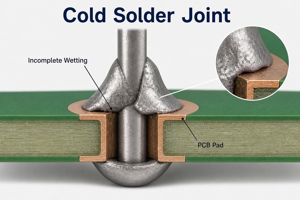
What Is a Cold Solder Joint?
A cold joint forms when the soldering operation does not establish the intended bond between solder and the surfaces being joined. Melting wire on an iron tip is not enough: the lead and pad must also reach suitable soldering conditions.
People often use the term for several different defects. That shorthand can send corrective action in the wrong direction. A connection that cracked after repeated thermal cycling, for example, does not prove that the original soldering temperature was too low.
| Condition | Defining issue | Investigation focus |
| Cold or incompletely formed joint | Inadequate joining conditions and poor bonding | Heat transfer, thermal history and flux performance |
| Non-wetting | Solder does not adhere to a surface | Oxidation, contamination, finish and thermal process |
| Disturbed joint | Movement during solidification disrupts the connection | Fixturing, handling and cooling |
| Insufficient solder | Too little solder for the required connection geometry | Deposit volume, wire feed or hole filling |
| Cracked joint | A fracture interrupts part or all of the connection | Mechanical load, fatigue, board flex and original workmanship |
Use the defect terminology and acceptance criteria specified for the assembly. IPC J-STD-001 addresses soldered-assembly requirements, while IPC-A-610 covers post-assembly acceptability. The agreed revision, product class, package geometry and customer requirements matter; an internet photograph is not a substitute.
Cold Solder Joint vs Good Solder Joint
The important comparison is bonding and joint geometry, not simply dull versus shiny. Inspect how solder meets the lead and land, whether there is a visible separation, and whether the connection meets its applicable requirements.
Lead-free joints can have a normal satin or matte appearance. Conversely, a reflective blob can conceal poor wetting underneath. A concave fillet is useful in many exposed leaded connections, but not every package should have the same profile.
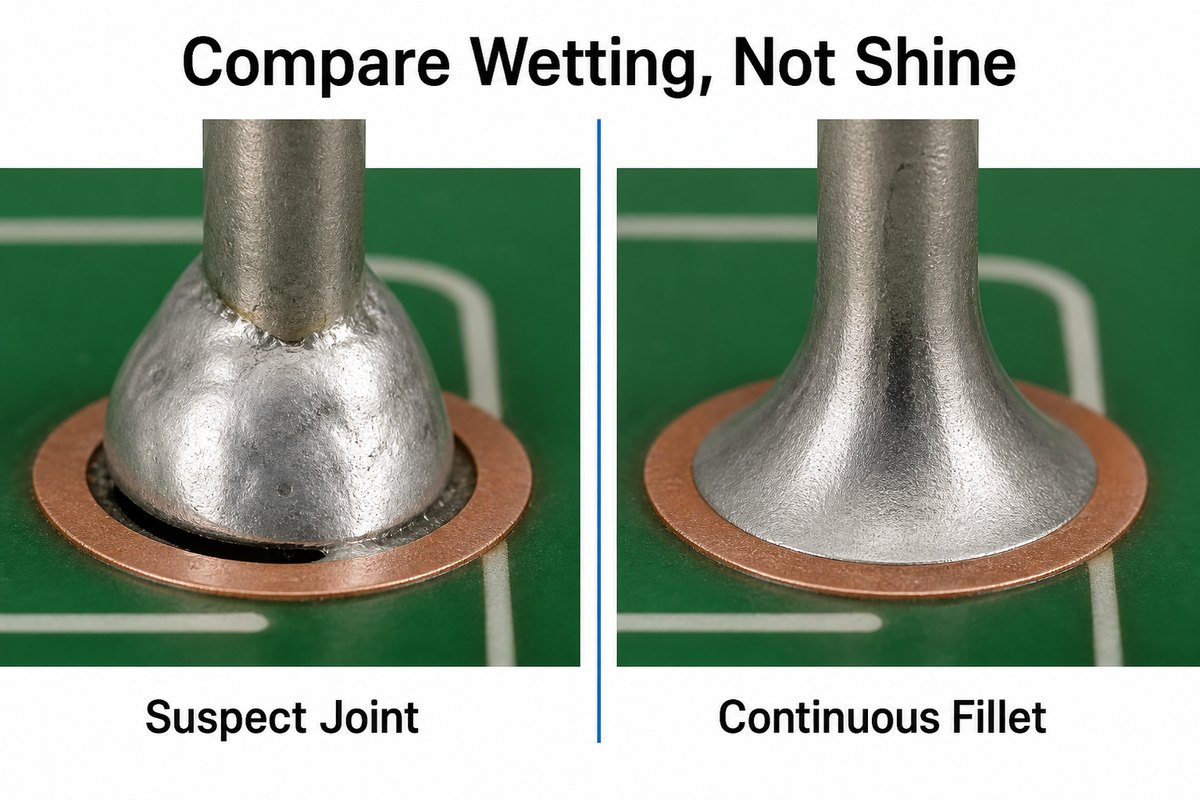
The illustrations here explain mechanisms; they are not actual inspection photographs or acceptance samples. For more detail on connection shape, see our solder fillet guide. Compare production findings with approved workmanship examples for the same alloy and component type.
Cold Solder Joint Symptoms
Possible symptoms include intermittent operation, abnormal resistance and a visible discontinuity, but none uniquely identifies a cold joint.
- Intermittent resets or signal loss: record the operating state, affected net and repeatability before disturbing the board.
- A voltage drop under load: investigate the complete current path, including connectors, traces and protection devices.
- A visible ring, gap or lifted interface: inspect from multiple angles and distinguish solder separation from a damaged land.
- Failures associated with temperature or vibration: consider cracked joints, connector contacts and component faults as competing explanations.
A continuity beep only shows that a conductive path exists under that test condition. It does not establish mechanical integrity or long-term reliability. Avoid flexing a powered board to make the fault appear; that can create new damage and obscure the original cause.
Why Can a Hot Iron Still Produce a Poor Joint?
The station setting is not the temperature reached by the lead and pad. A small tip, oxidized contact surface or large copper heat sink can prevent adequate heat transfer even when the displayed setting looks high.
Check tip condition, contact area and recovery under load before increasing temperature. Heating only the solder wire can leave the board interface too cool. At the other extreme, prolonged contact can damage lands, components or finishes.
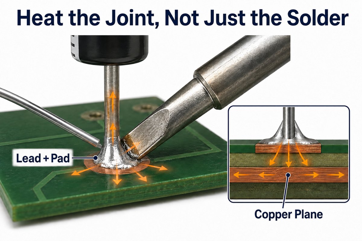
A ground-connected connector pin and a small isolated signal pin may need different validated techniques. Tip geometry, equipment capacity and controlled preheating can be more useful than a hotter setting. Apply component and board thermal limits; there is no single iron temperature or contact time suitable for every assembly.
Which Material Conditions Can Prevent Wetting?
Oxidized or contaminated surfaces and unsuitable flux conditions can prevent solder from wetting even when heat delivery is adequate.
- PCB finish: examine storage, handling, finish condition and whether defects follow a board lot.
- Component termination: compare date codes and lots, especially when one component type fails across several boards.
- Solder and flux: confirm approved alloy, flux compatibility, expiry and handling requirements.
- Paste exposure: follow the manufacturer’s storage, warming, mixing and usable-life instructions rather than an improvised shop-floor rule.
Do not automatically compensate for poor solderability with stronger flux or more flux. Those changes can affect residue, cleaning and electrical reliability requirements. Confirm the suspected input through controlled comparison and, where appropriate, a specified solderability evaluation.
How Do SMT and Through-Hole Investigations Differ?
SMT reflow, wave or selective soldering, and hand soldering deliver heat differently, so their process evidence should not be mixed.
| Assembly process | First records to review | Useful comparison |
| SMT reflow | Measured board profile, paste lot and handling, printing and placement results | Affected package locations versus thermal mass and deposit consistency |
| Wave or selective soldering | Flux application, preheat, solder contact and pallet or nozzle setup | Problem pins versus copper connections, access and hole-fill pattern |
| Hand soldering | Tip condition, equipment recovery, technique and material identification | Results by joint geometry, station and operator |
For reflow, measure representative joint locations on the actual assembly. An oven recipe or chamber temperature is not a board profile. Use the solder-paste process window together with component and laminate limits, and verify the effect of board loading or fixture changes.
Solder paste inspection can identify printing problems before placement, but it cannot prove that the later reflow process formed a sound connection. Similarly, poor through-hole fill does not by itself identify a cold joint. Our overview of PCB board soldering methods explains where the different processes fit.
How Should a Suspect Connection Be Inspected?
Combine the failure history with inspection and electrical evidence. Each method answers a different question.
- Visual inspection or AOI: examines accessible geometry and visible workmanship; hidden interfaces remain outside the view.
- X-ray: helps assess hidden solder distribution, bridges and certain voids or opens. A normal-looking image does not by itself establish metallurgical bonding.
- Electrical testing: checks the circuit under defined conditions. Coverage depends on access, test limits and the fault’s repeatability.
- Targeted failure analysis: sectioning or other specialist methods may be needed when the interface cannot be resolved non-destructively.
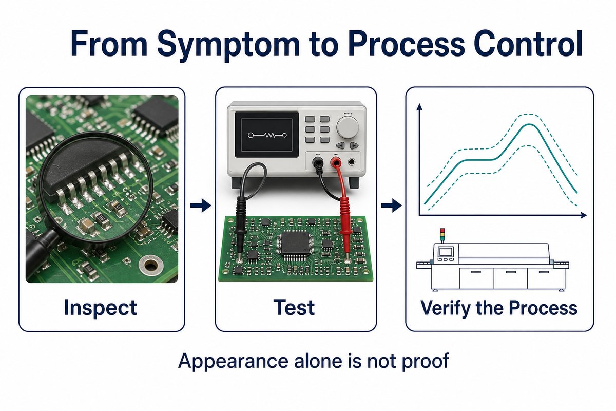
Plan destructive analysis before consuming the only failed sample. Preserve photographs, reference designators, test logs and an untouched comparison board where possible. Select methods according to the suspected failure, not because an inspection machine is available. Our PCB testing guide provides broader context on test coverage.
How Can the Root Cause Be Narrowed Down?
Group failures by shared process inputs before changing settings. A pattern across lots, stations or board locations can be more informative than the appearance of one joint.
Consider an illustrative investigation: connector pins connected to a large copper area fail inspection, while nearby signal pins do not. That pattern supports checking heat delivery and thermal mass. If the same termination fails on different board designs but only from one component lot, solderability becomes a stronger hypothesis. Neither pattern is proof until tested.
- Identify affected assemblies, reference designators, lots and process steps.
- Preserve the original condition and confirm that the reported fault is reproducible.
- Select the most plausible cause from physical and process evidence.
- Change a controlled input and compare results against an unchanged reference.
- Verify the correction on subsequent production, not just the repaired sample.
Keep containment separate from corrective action. Screening a suspect lot may reduce escapes, but it does not explain why the defect occurred or prevent another lot from repeating it.
Cold Solder Joint Repair
Repair should restore the required connection without exceeding the assembly’s rework limits. Blindly reheating every dull joint can damage otherwise acceptable work and erase useful failure evidence.
Qualified personnel should isolate power, discharge stored energy through an approved procedure and use appropriate ESD protection and fume extraction. Battery-connected, high-voltage and safety-critical assemblies need product-specific precautions.
- Confirm whether the defect is solder-related or involves a lifted land, damaged barrel, component or trace.
- Use an approved procedure with compatible alloy, flux, tools and thermal limits.
- Remove or replace solder and components when the diagnosed condition requires it; do not simply add a larger mound.
- Clean when required by the flux and assembly specification, then inspect and retest.
- Record rework history and disposition. Quarantine assemblies that cannot meet requirements without further damage.
For a broader introduction to identification and repair, see our existing cold-joint meaning, symptoms and prevention guide. Production release still requires the agreed acceptance criteria and test plan.
How Can Recurring Defects Be Prevented?
Control the inputs that caused the failure and verify their stability over time. Inspection alone is not a substitute for a capable soldering process.
Practical controls include material traceability, documented storage conditions, maintained soldering equipment, validated profiles and fixtures, and training matched to the actual joint types. Review defect trends after changes to component suppliers, board copper distribution, panel layout or tooling.
On the design side, review soldering access, copper heat sinking and mechanical loads with the assembly team. Thermal relief may help some connections, but current capacity, heat flow and reliability requirements can justify solid connections. The right choice is a design-and-process decision, not a universal rule.
FAQ About Cold Solder Joints
Can a cold joint pass a continuity test? Yes. A conductive path can exist at the moment of testing even if the connection is unreliable. Test results must be interpreted alongside workmanship and the actual failure conditions.
Is every dull lead-free joint bad? No. Alloy composition and solidification affect appearance. Inspect wetting, geometry and defects against the applicable criteria rather than using surface shine as the acceptance rule.
Does a temperature-sensitive fault prove a cold joint? No. Cracks, connectors and components can also produce temperature-dependent failures. Preserve the symptom, localize the affected circuit and test competing explanations.
Will adding flux and reheating always solve it? No. Contaminated surfaces, damaged pads, unsuitable materials or later fatigue may need a different response. Rework should follow diagnosis and an approved procedure.
Is a cold joint the same as a cracked joint? No. The first describes inadequate joint formation; the second describes a fracture. They may coexist, but a crack alone does not establish the original manufacturing cause.
How Can EBest Circuit Support Your PCB Assembly?
At EBest Circuit, we provide PCB fabrication and PCBA services, with inspection capabilities including SPI, AOI and X-ray. We can review your board layout, assembly requirements and proposed inspection coverage together, so soldering risks are considered before production rather than only after a failed board appears.
If you are investigating a cold solder joint issue or preparing a new assembly, send your Gerber files, BOM, quantity and testing requirements to sales@bestpcbs.com. For an existing failure, include clear photographs, reference designators and the conditions that reproduce it. We will review the project requirements and discuss the appropriate manufacturing and inspection scope.