PCB manufacturing PCB manufacturing
Home > Blog

cold solder joint symptoms

Cold Solder Joint in PCB Assembly: Root Causes and Process Control
Thursday, September 3rd, 2026

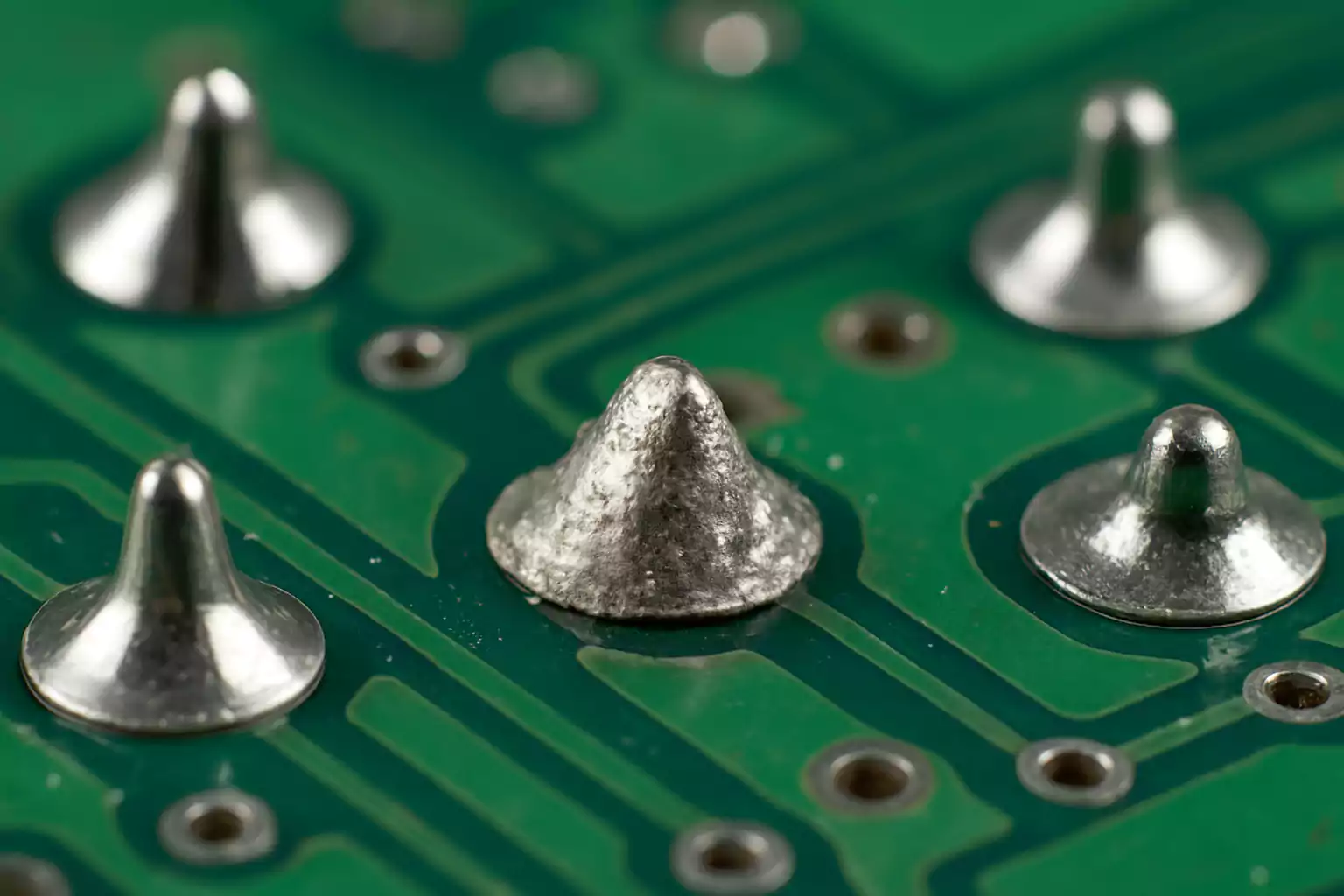
A cold solder joint is an inadequately formed solder connection, commonly associated with insufficient heat at the joining surfaces and poor wetting. It can create an open circuit, elevated resistance, or an intermittent fault. However, a dull surface alone does not establish that a joint is defective, especially with lead-free alloys.

For a production team, finding a suspect joint is only the start. The useful question is whether it came from heat delivery, surface condition, material handling, movement, or a later mechanical failure. This guide focuses on separating those causes so that a repaired board does not return with the same problem.
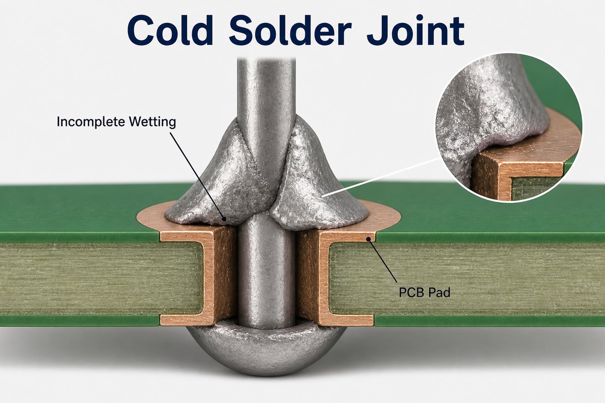
Cold Solder Joint conceptual PCB cutaway showing incomplete wetting at a pad

What Is a Cold Solder Joint?

A cold joint forms when the soldering operation does not establish the intended bond between solder and the surfaces being joined. Melting wire on an iron tip is not enough: the lead and pad must also reach suitable soldering conditions.

People often use the term for several different defects. That shorthand can send corrective action in the wrong direction. A connection that cracked after repeated thermal cycling, for example, does not prove that the original soldering temperature was too low.

Condition Defining issue Investigation focus
Cold or incompletely formed joint Inadequate joining conditions and poor bonding Heat transfer, thermal history and flux performance
Non-wetting Solder does not adhere to a surface Oxidation, contamination, finish and thermal process
Disturbed joint Movement during solidification disrupts the connection Fixturing, handling and cooling
Insufficient solder Too little solder for the required connection geometry Deposit volume, wire feed or hole filling
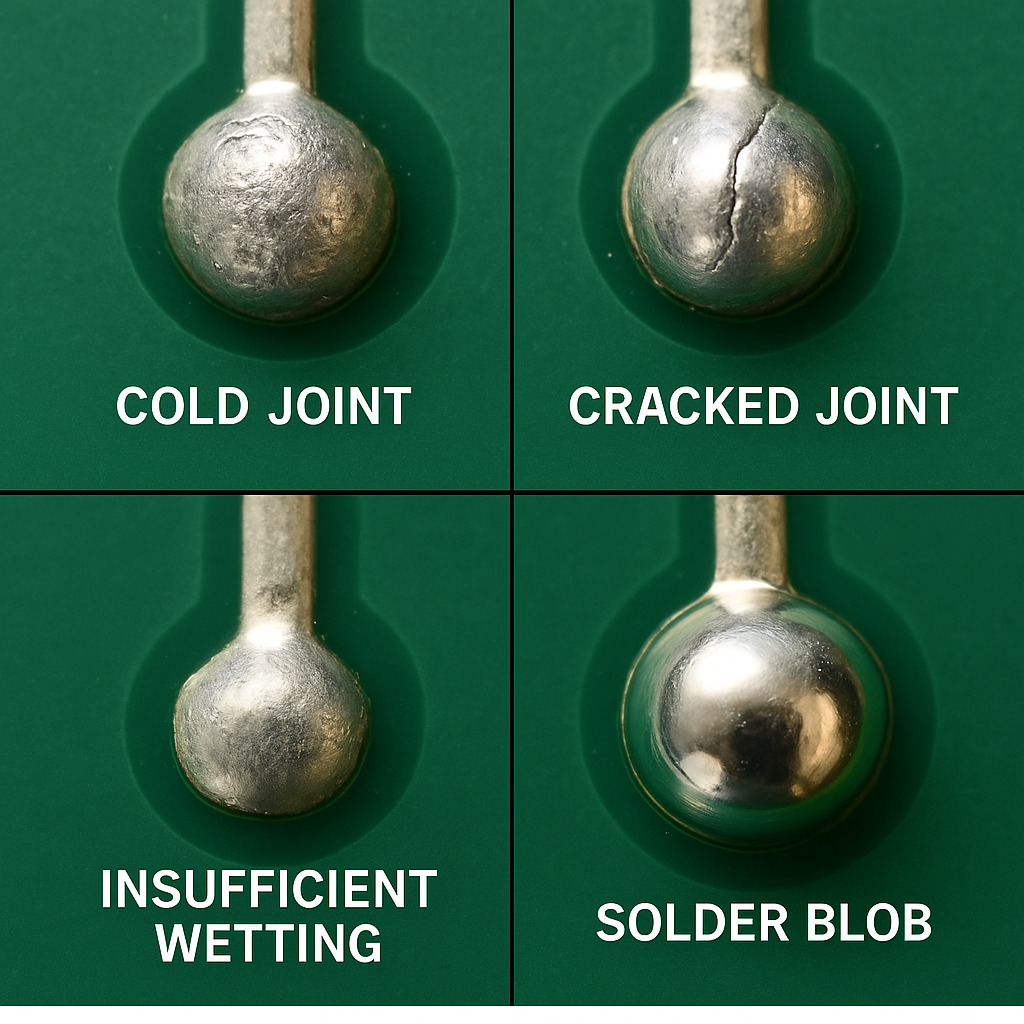
Cracked joint A fracture interrupts part or all of the connection Mechanical load, fatigue, board flex and original workmanship

Use the defect terminology and acceptance criteria specified for the assembly. IPC J-STD-001 addresses soldered-assembly requirements, while IPC-A-610 covers post-assembly acceptability. The agreed revision, product class, package geometry and customer requirements matter; an internet photograph is not a substitute.

Cold Solder Joint vs Good Solder Joint

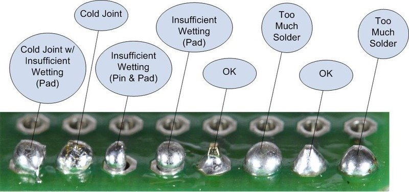
The important comparison is bonding and joint geometry, not simply dull versus shiny. Inspect how solder meets the lead and land, whether there is a visible separation, and whether the connection meets its applicable requirements.

Lead-free joints can have a normal satin or matte appearance. Conversely, a reflective blob can conceal poor wetting underneath. A concave fillet is useful in many exposed leaded connections, but not every package should have the same profile.
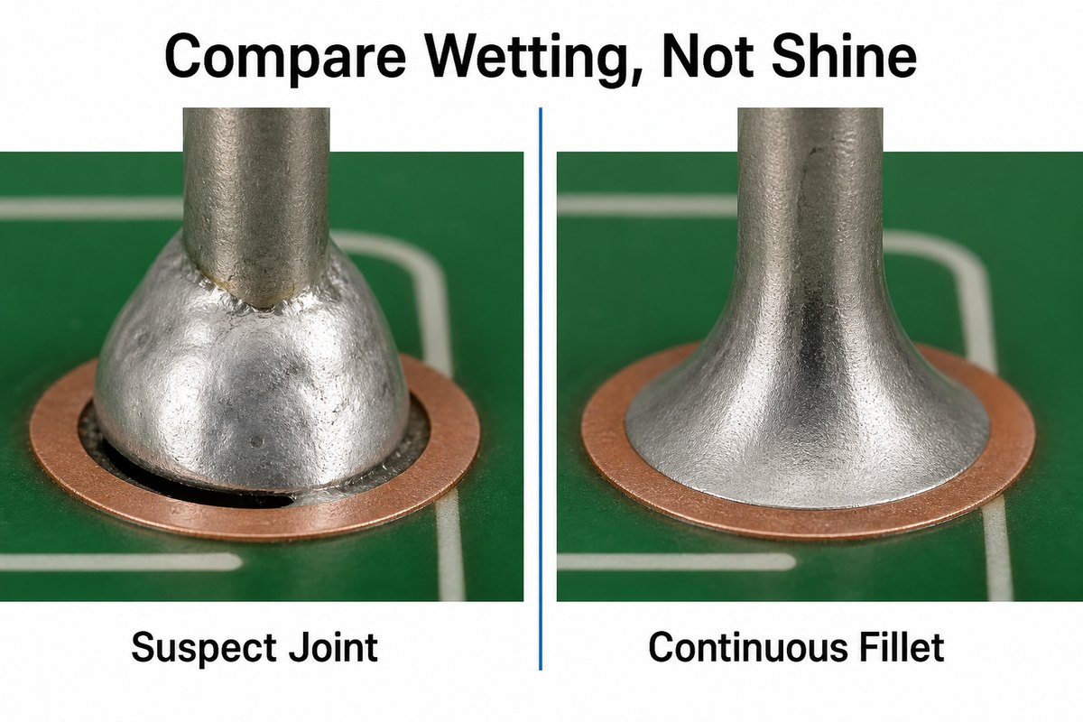
Conceptual comparison of an unwetted solder gap and a continuous solder fillet

The illustrations here explain mechanisms; they are not actual inspection photographs or acceptance samples. For more detail on connection shape, see our solder fillet guide. Compare production findings with approved workmanship examples for the same alloy and component type.

Cold Solder Joint Symptoms

Possible symptoms include intermittent operation, abnormal resistance and a visible discontinuity, but none uniquely identifies a cold joint.

  • Intermittent resets or signal loss: record the operating state, affected net and repeatability before disturbing the board.
  • A voltage drop under load: investigate the complete current path, including connectors, traces and protection devices.
  • A visible ring, gap or lifted interface: inspect from multiple angles and distinguish solder separation from a damaged land.
  • Failures associated with temperature or vibration: consider cracked joints, connector contacts and component faults as competing explanations.

A continuity beep only shows that a conductive path exists under that test condition. It does not establish mechanical integrity or long-term reliability. Avoid flexing a powered board to make the fault appear; that can create new damage and obscure the original cause.

Why Can a Hot Iron Still Produce a Poor Joint?

The station setting is not the temperature reached by the lead and pad. A small tip, oxidized contact surface or large copper heat sink can prevent adequate heat transfer even when the displayed setting looks high.

Check tip condition, contact area and recovery under load before increasing temperature. Heating only the solder wire can leave the board interface too cool. At the other extreme, prolonged contact can damage lands, components or finishes.
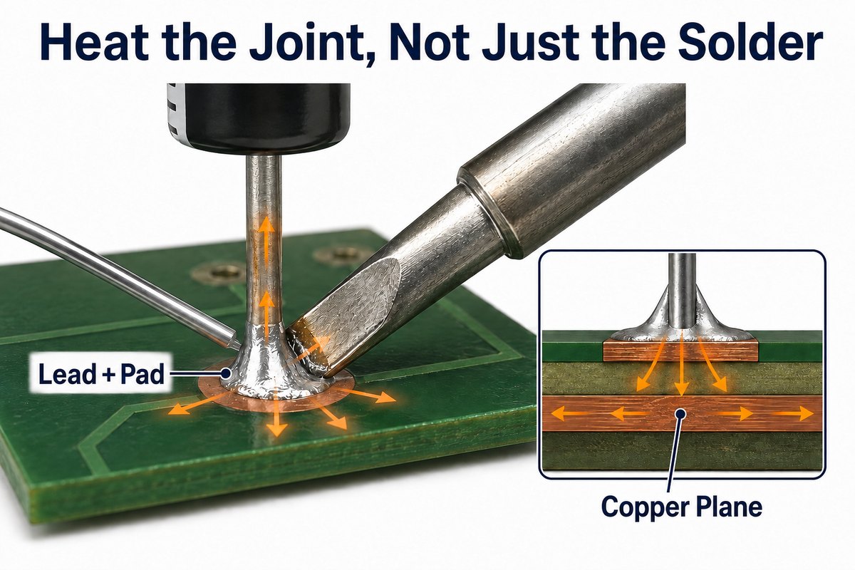
Soldering tip heating the lead and pad with an inset showing heat spreading through copper

A ground-connected connector pin and a small isolated signal pin may need different validated techniques. Tip geometry, equipment capacity and controlled preheating can be more useful than a hotter setting. Apply component and board thermal limits; there is no single iron temperature or contact time suitable for every assembly.

Which Material Conditions Can Prevent Wetting?

Oxidized or contaminated surfaces and unsuitable flux conditions can prevent solder from wetting even when heat delivery is adequate.

  • PCB finish: examine storage, handling, finish condition and whether defects follow a board lot.
  • Component termination: compare date codes and lots, especially when one component type fails across several boards.
  • Solder and flux: confirm approved alloy, flux compatibility, expiry and handling requirements.
  • Paste exposure: follow the manufacturer’s storage, warming, mixing and usable-life instructions rather than an improvised shop-floor rule.

Do not automatically compensate for poor solderability with stronger flux or more flux. Those changes can affect residue, cleaning and electrical reliability requirements. Confirm the suspected input through controlled comparison and, where appropriate, a specified solderability evaluation.

How Do SMT and Through-Hole Investigations Differ?

SMT reflow, wave or selective soldering, and hand soldering deliver heat differently, so their process evidence should not be mixed.

Assembly process First records to review Useful comparison
SMT reflow Measured board profile, paste lot and handling, printing and placement results Affected package locations versus thermal mass and deposit consistency
Wave or selective soldering Flux application, preheat, solder contact and pallet or nozzle setup Problem pins versus copper connections, access and hole-fill pattern
Hand soldering Tip condition, equipment recovery, technique and material identification Results by joint geometry, station and operator

For reflow, measure representative joint locations on the actual assembly. An oven recipe or chamber temperature is not a board profile. Use the solder-paste process window together with component and laminate limits, and verify the effect of board loading or fixture changes.

Solder paste inspection can identify printing problems before placement, but it cannot prove that the later reflow process formed a sound connection. Similarly, poor through-hole fill does not by itself identify a cold joint. Our overview of PCB board soldering methods explains where the different processes fit.

How Should a Suspect Connection Be Inspected?

Combine the failure history with inspection and electrical evidence. Each method answers a different question.

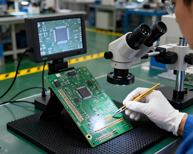
  • Visual inspection or AOI: examines accessible geometry and visible workmanship; hidden interfaces remain outside the view.
  • X-ray: helps assess hidden solder distribution, bridges and certain voids or opens. A normal-looking image does not by itself establish metallurgical bonding.
  • Electrical testing: checks the circuit under defined conditions. Coverage depends on access, test limits and the fault’s repeatability.
  • Targeted failure analysis: sectioning or other specialist methods may be needed when the interface cannot be resolved non-destructively.
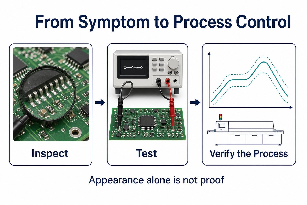
Inspection, electrical testing and process verification combined in a solder-joint investigation

Plan destructive analysis before consuming the only failed sample. Preserve photographs, reference designators, test logs and an untouched comparison board where possible. Select methods according to the suspected failure, not because an inspection machine is available. Our PCB testing guide provides broader context on test coverage.

How Can the Root Cause Be Narrowed Down?

Group failures by shared process inputs before changing settings. A pattern across lots, stations or board locations can be more informative than the appearance of one joint.

Consider an illustrative investigation: connector pins connected to a large copper area fail inspection, while nearby signal pins do not. That pattern supports checking heat delivery and thermal mass. If the same termination fails on different board designs but only from one component lot, solderability becomes a stronger hypothesis. Neither pattern is proof until tested.

  1. Identify affected assemblies, reference designators, lots and process steps.
  2. Preserve the original condition and confirm that the reported fault is reproducible.
  3. Select the most plausible cause from physical and process evidence.
  4. Change a controlled input and compare results against an unchanged reference.
  5. Verify the correction on subsequent production, not just the repaired sample.

Keep containment separate from corrective action. Screening a suspect lot may reduce escapes, but it does not explain why the defect occurred or prevent another lot from repeating it.

Cold Solder Joint Repair

Repair should restore the required connection without exceeding the assembly’s rework limits. Blindly reheating every dull joint can damage otherwise acceptable work and erase useful failure evidence.

Qualified personnel should isolate power, discharge stored energy through an approved procedure and use appropriate ESD protection and fume extraction. Battery-connected, high-voltage and safety-critical assemblies need product-specific precautions.

  • Confirm whether the defect is solder-related or involves a lifted land, damaged barrel, component or trace.
  • Use an approved procedure with compatible alloy, flux, tools and thermal limits.
  • Remove or replace solder and components when the diagnosed condition requires it; do not simply add a larger mound.
  • Clean when required by the flux and assembly specification, then inspect and retest.
  • Record rework history and disposition. Quarantine assemblies that cannot meet requirements without further damage.

For a broader introduction to identification and repair, see our existing cold-joint meaning, symptoms and prevention guide. Production release still requires the agreed acceptance criteria and test plan.

How Can Recurring Defects Be Prevented?

Control the inputs that caused the failure and verify their stability over time. Inspection alone is not a substitute for a capable soldering process.

Practical controls include material traceability, documented storage conditions, maintained soldering equipment, validated profiles and fixtures, and training matched to the actual joint types. Review defect trends after changes to component suppliers, board copper distribution, panel layout or tooling.

On the design side, review soldering access, copper heat sinking and mechanical loads with the assembly team. Thermal relief may help some connections, but current capacity, heat flow and reliability requirements can justify solid connections. The right choice is a design-and-process decision, not a universal rule.

FAQ About Cold Solder Joints

Can a cold joint pass a continuity test? Yes. A conductive path can exist at the moment of testing even if the connection is unreliable. Test results must be interpreted alongside workmanship and the actual failure conditions.

Is every dull lead-free joint bad? No. Alloy composition and solidification affect appearance. Inspect wetting, geometry and defects against the applicable criteria rather than using surface shine as the acceptance rule.

Does a temperature-sensitive fault prove a cold joint? No. Cracks, connectors and components can also produce temperature-dependent failures. Preserve the symptom, localize the affected circuit and test competing explanations.

Will adding flux and reheating always solve it? No. Contaminated surfaces, damaged pads, unsuitable materials or later fatigue may need a different response. Rework should follow diagnosis and an approved procedure.

Is a cold joint the same as a cracked joint? No. The first describes inadequate joint formation; the second describes a fracture. They may coexist, but a crack alone does not establish the original manufacturing cause.

How Can EBest Circuit Support Your PCB Assembly?

At EBest Circuit, we provide PCB fabrication and PCBA services, with inspection capabilities including SPI, AOI and X-ray. We can review your board layout, assembly requirements and proposed inspection coverage together, so soldering risks are considered before production rather than only after a failed board appears.

If you are investigating a cold solder joint issue or preparing a new assembly, send your Gerber files, BOM, quantity and testing requirements to sales@bestpcbs.com. For an existing failure, include clear photographs, reference designators and the conditions that reproduce it. We will review the project requirements and discuss the appropriate manufacturing and inspection scope.
You may also like

What Is a Cold Solder Joint? Cold Solder Joint vs Good Solder Joint
Friday, January 2nd, 2026

A cold solder joint is one of the most common failure mechanisms in electronics assembly, yet many technicians and engineers encounter it long before fully understanding its root behaviors. When a joint lacks proper heat, does not wet the copper pad, or cools in an uncontrolled manner, the resulting connection becomes unstable. It may pass initial testing, but its long-term reliability declines.

Because modern electronics demand consistent performance—whether in consumer devices, industrial controllers, automotive modules, or medical PCB assemblies—recognizing and preventing cold solder joints remains essential for every design or manufacturing team.

What Is a Cold Solder Joint?

A cold solder joint is a solder connection that forms without reaching the proper temperature for the solder alloy to fully melt, flow, and wet the surfaces. Instead of a smooth, solidly bonded joint, the resulting structure becomes dull, grainy, or cracked. The term “cold” comes from the fact that these joints never reach the temperature required to create a metallurgical bond between the solder and the copper pad or component lead.

In practical terms, the solder solidifies before forming a stable interface. Instead of integrating with the metals it is meant to join, it merely sits on top of the surfaces. The joint may appear attached, but internally it lacks the uniform crystalline structure that defines a reliable connection.

In manual soldering, cold joints often happen due to inconsistent technique. In automated SMT production, they typically arise from incorrect reflow profiles, insufficient preheat, or contaminated pads that prevent proper wetting. Because of these variables, avoiding cold solder joints requires both strong process control and clean material handling.

What Is a Cold Solder Joint? Cold Solder Joint vs Good Solder Joint

Do Cold Solder Joints Still Work?

A cold solder joint may still work, at least at the beginning. This is where confusion begins for many technicians. The joint may pass functional testing, power-on checks, or a quick continuity test. Because the mechanical bond is weak and the electrical interface incomplete, the behavior becomes intermittent.

A device with cold joints may operate well in a static environment but become unstable when exposed to:

  • Temperature swings
  • Vibration or shock
  • Thermal expansion during operation
  • Humidity or oxidation
  • Long-term cycling

While a cold joint can conduct current, it does so inconsistently, and usually with higher resistance. Over time, micro-cracks grow, creating open circuits or signal noise. For that reason, cold solder joints are considered functional only by coincidence, not by design.

Cold Solder Joint Symptoms

Cold solder joints have predictable symptoms. Engineers often rely on these visual or electrical clues to locate the root cause of a circuit failure:

  • Dull, Frosty, or Grainy Surface
  • Irregular Shape or Incomplete Wetting
  • Visible Cracks or Rings
  • Intermittent Performance
  • Increased Resistance
  • Movement When Touched
  • Failure Under Thermal Stress
Cold Solder Joint Symptoms

These symptoms are reliable indicators during repair, inspection, or failure analysis.

What Is the Difference Between a Cold Solder Joint and a Good Solder Joint?

A good solder joint forms a solid intermetallic bond between the solder, the copper pad, and the component lead. It exhibits a smooth, shiny, and uniform shape with complete wetting.

Comparing both joints helps clarify the contrast:

AspectCold Solder JointGood Solder Joint
AppearanceDull, grainy, frosty surfaceSmooth, shiny, uniform surface
Wetting BehaviorPoor wetting; solder sits on top of pad/leadComplete wetting across pad and lead
Mechanical StrengthWeak bond; prone to cracking or movementStrong bond with stable mechanical support
Electrical PerformanceHigher resistance; intermittent continuityLow resistance; stable, consistent conductivity
ReliabilityUnpredictable; often fails under vibration or heatLong-lasting; passes thermal and vibration stress
Internal StructureIncomplete metallurgical bond; voids possibleProper intermetallic layer with solid structure
Common CausesInsufficient heat, oxidized surfaces, poor flux activityCorrect temperature, clean pads, controlled soldering
Inspection ResultRejected under IPC standardsAcceptable and compliant with IPC criteria
Typical SymptomsIntermittent signals, device resets, heat spotsNormal operation with steady performance
Corrective ActionReheat, add flux, reflow or resolderNo action required

How to Identify a Cold Solder Joint?

Identifying cold solder joints requires a combination of visual inspection, tactile testing, and electrical measurement. Here are the most common methods:

  • Visual Inspection

Under a microscope or magnifying lamp, look for dull surfaces, cracks, uneven shapes, or insufficient solder spread. Most cold joints are visible to a trained eye.

  • Continuity and Resistance Testing

Using a multimeter, check whether current flows consistently. Cold joints may pass continuity tests but show higher resistance.

  • Thermal Stress Testing

Heating or cooling the PCB may cause the joint to open or reconnect.

  • X-ray Inspection (for BGA or QFN)

In high-density packages, internal cold joints appear as voids, incomplete wetting, or irregular solder shapes.

  • Mechanical Movement

Applying gentle pressure can reveal looseness in through-hole components.

Early identification is essential in avoiding expensive rework or device failure.

How to Identify a Cold Solder Joint?

Are Cold Joints Acceptable?

Cold solder joints are not acceptable in any professional electronics assembly environment. Industry standards such as IPC-A-610 define cold joints as defects requiring correction. Even in hobby projects, cold joints degrade reliability.

There are no scenarios where cold joints are intentionally tolerated. Any sign of incomplete wetting or insufficient flow must be corrected immediately. or mission-critical industries such as:

  • Medical
  • Automotive
  • Industrial automation
  • Aerospace
  • IoT
  • Telecommunications

cold solder joints represent unacceptable risk.

What Causes a Cold Solder Joint?

Cold solder joints form due to several common process issues. Understanding these causes helps prevent recurrence.

1. Insufficient Heat

If the soldering iron does not fully heat the pad and lead, wetting cannot occur.

2. Contaminated or Oxidized Surfaces

Residue, dust, oxide layers, or aged plating can block wetting.

3. Incorrect Solder Alloy or Temperature

Low heat settings, mismatched solder types, or incorrect thermal profiles lead to poor flow.

4. Poor Flux Activity

Flux cleans surfaces. Weak or expired flux prevents proper bonding.

5. Movement During Solidification

If the lead moves before the solder cools, a cold joint forms.

6. Inconsistent Reflow Profile

In SMT production, a poorly tuned reflow oven produces cold joints, especially on large thermal pads or ground planes.

7. Manual Soldering Technique Errors

Rushed or inconsistent soldering practices can create joints that never heat sufficiently.

What Are the Risks of Cold Joints?

Cold solder joints introduce multiple failure modes, including:

1. The device may work partially, only under specific temperature or vibration conditions.

2. Higher resistance destabilizes signals, especially in RF or high-speed digital designs.

3. Poor conductivity forces current to generate heat, stressing components.

4. Cold joints often degrade quickly in real-world conditions.

5. In power electronics, cold joints increase the risk of arcing or thermal runaway.

These risks emphasize the need for controlled soldering conditions, proper inspection, and strict quality assurance.

How to Avoid Cold Solder Joints?

Preventing cold solder joints requires strong process management, skilled operators, and adherence to IPC and manufacturer guidelines.

1. Ensure Proper Heating

Heat both pad and lead evenly. Maintain appropriate soldering temperatures for the chosen alloy.

2. Use High-Quality Solder and Fresh Flux

Materials is important, Fresh flux ensures clean surfaces and stable wetting.

3. Clean and Prepare Surfaces

Remove oxidation, oil, or contamination before soldering.

4. Maintain Stable Reflow Profiles

For SMT production, program time-temperature profiles to match the alloy. Adjust for heavy copper or large thermal pads.

5. Avoid Movement During Cooling

Secure components so solder can solidify without vibration.

6. Use Proper Tools

ESD-safe irons, clean tips, good tweezers, and inspection magnification help ensure accuracy.

7. Follow IPC Guidelines

Standards such as IPC-A-610 and IPC-J-STD-001 provide industry-accepted criteria for solder quality.

Understanding the distinction between a cold solder joint and a properly formed one helps engineers and technicians diagnose failures accurately. A cold solder joint appears dull, weak, and inconsistent, while a good joint is smooth, shiny, and electrically stable. The difference directly affects device performance and lifespan.

As electronics continue shrinking and integrating more complex components, the need for reliable soldering becomes even more critical. Whether you are working with prototype boards, high-density PCBs, or mission-critical assemblies, eliminating cold joints should always be a priority.

You may also like

What Is a Cold Solder Joint? Meaning, Symptoms, Repair & Prevention Guide
Friday, January 2nd, 2026

A cold solder joint is one of the most common reliability defects in PCB and PCBA assemblies, and it continues to be a major source of intermittent failures across consumer electronics, industrial controls, medical devices, automotive modules, and aerospace hardware. At Best Technology, we see the long-term consequences of cold joints in incoming failure analyses from global customers—especially in assemblies where stable conductivity and mechanical strength are critical.

With 19 years of PCBA production experience across China and Vietnam, medical-grade and aerospace-grade certifications, and MES-controlled SMT lines, we understand how cold solder joints emerge, how to eliminate them, and how to engineer assemblies that remain stable throughout the product life cycle.

What Is a Cold Solder Joint?

A cold solder joint forms when solder does not melt or wet the pad and component lead completely. Instead of creating a unified bond, the solder cools prematurely or never flows correctly, resulting in a dull, grainy, or uneven connection.

In the PCBA environment, cold joints are considered a process defect because they weaken the mechanical integrity of a soldered connection and create unstable electrical performance that deteriorates over time.

In high-reliability sectors—medical, industrial, aerospace—these defects are unacceptable and must be removed at the root cause: temperature control, surface condition, solder alloy behavior, and wetting characteristics.

What Is a Cold Solder Joint? Meaning, Symptoms, Repair & Prevention Guide

Do Cold Solder Joints Still Work?

Temporarily, yes. Reliably, no. A cold solder joint may appear functional during a quick test, then fail:

  • When the board heats during normal operation
  • When vibration or slight mechanical stress occurs
  • When humidity or temperature cycles change contact resistance
  • When current load increases

This unstable behavior is what makes cold joints one of the most misdiagnosed failure sources. Many customers approach Best Technology believing they have a “component issue” or “firmware bug,” when the real cause is inconsistent solder metallurgy.

Cold Solder Joint Symptoms

From a PCBA viewpoint, cold joints create early-life failures that escalate under stress. Common symptoms include:

  • Intermittent booting or power instability
  • Flickering LEDs, displays, or inconsistent sensor readings
  • Weak or noisy signals in communication lines
  • Overheating around a soldered component
  • Boards that only work when pressed or tapped
  • Modules that behave differently under temperature changes

During incoming quality analysis at Best Technology, we often find that unstable BGA balls, hand-soldered connectors, and TH pins are common locations for cold joints.

Cold Solder Joint Symptoms

What Is the Difference Between a Cold Solder Joint and a Good Solder Joint?

A good solder joint creates a smooth, bright, and uniform connection that wraps around the lead with full wetting.

A cold joint typically shows:

  • A dull or matte finish
  • Crystalline or grainy texture
  • A ring fracture around the lead
  • A small gap between solder and pad
  • Solder balled up instead of flowing

Experienced technicians immediately recognize these visual cues because they suggest weak mechanical support and unstable electrical conductivity.

How to Identify a Cold Solder Joint?

Both technicians and advanced PCBA factories rely on a few inspection methods:

  • Bright-light and angled inspection to reveal dull or frosted surfaces
  • Magnification to highlight cracks or gaps
  • Gentle mechanical pressure to detect movement
  • Thermal testing to expose resistance changes under heat
  • AOI or X-ray for lead-free and hidden joints
How to Identify a Cold Solder Joint?

In Best Technology’s MES-controlled lines, each soldering step—including reflow, wave, and selective solder—is tied to traceable profiles, making it easier to isolate and prevent cold joints during future builds.

Are Cold Joints Acceptable?

No. Cold solder joints are never acceptable in professional electronics.

They violate:

  • IPC-A-610 standards
  • Reliability requirements
  • Safety and quality regulations

Even in low-cost consumer electronics, cold joints significantly reduce product lifespan and reliability.

What Causes a Cold Solder Joint?

Cold solder joints originate from several process-related or operator-related factors:

  • Insufficient soldering temperature
  • Iron tip or nozzle unable to deliver stable heat
  • Oxidized pads, leads, or old components
  • Expired or poorly stored solder paste
  • Flux burnout or inadequate flux coating
  • Component movement during cooling
  • Large copper areas absorbing heat too fast
  • Incorrect reflow curve in SMT production

With our dual factories in China and Vietnam, Best Technology maintains strict humidity control, paste storage, stencil management, and reflow calibration—reducing these risks dramatically.

What Are the Risks of Cold Joints?

Cold solder joints introduce cascading reliability issues:

  • Intermittent electrical contact
  • Overheating of stressed joints
  • Noise, distortion, or unstable signals
  • Sudden shutdowns during operation
  • Premature component failure
  • Total system outages in critical environments

In medical, industrial, and aerospace PCBAs, even a single cold joint is considered a critical defect (CD level). Best Technology screens aggressively to ensure these defects never leave the factory.

How to Fix a Cold Solder Joint?

Repair is direct, but must be done properly:

1. Clean the joint with isopropyl alcohol.

2. Apply quality flux to re-activate the surface.

3. Reheat the joint until solder melts fully.

4. Add a small amount of fresh solder if needed.

5. Allow full cooling without movement.

6. Inspect visually to ensure proper fillet and wetting.

For SMD components (QFN, BGA, LGA), reflow or hot-air rework ensures even heating.

How to Avoid Cold Solder Joints?

Prevention stems from controlled process engineering:

  • Use calibrated, temperature-controlled soldering equipment
  • Maintain component and PCB cleanliness
  • Follow correct reflow temperature profiles
  • Apply flux or paste with proper wetting characteristics
  • Preheat heavy copper boards
  • Avoid vibration during cooling
  • Use AOI/X-ray to verify solder integrity
  • Enforce operator training and certification

At Best Technology, these practices are embedded into MES workflows, ensuring traceability and repeatability—from prototype to mass production.

FAQ About Cold Solder Joint

1. Can flux prevent cold solder joints?

    Flux improves wetting, but without proper temperature, cold joints still occur.

    2. Can a cold solder joint cause a short?

    Yes. Cracking or partial bonding may create unintended bridges.

    3. Why are cold solder joints more common in lead-free solder?

    Lead-free alloys require higher melting temperatures and tighter process control.

    4. Can a multimeter detect a cold solder joint?

    Sometimes, but intermittent faults often remain hidden until the board is heated or flexed.

    5. Can reheating permanently fix a cold solder joint?

    If the pad and lead are clean and properly wetted, reheating provides a permanent repair.

    6. Do professional PCBA manufacturers still encounter cold joints?

    Rarely, but only because inspection systems, controlled processes, and trained operators keep solder quality consistent.

    When to Consult a Professional or a PCBA Manufacturer?

    If your board shows repeated failures, unstable behavior, or numerous questionable joints, professional evaluation is the safest choice. Best Technology supports global customers with:

    • In-house FA (failure analysis)
    • X-ray and AOI inspection
    • Controlled reflow soldering
    • Medical-grade and aerospace-grade quality systems
    • MES-tracked production across China and Vietnam

    Whether you need prototype repair, DFX recommendations, or full PCBA manufacturing, our engineering teams ensure solder reliability at every stage of the product life cycle.

    You may also like