PCB manufacturing PCB manufacturing
Home > Blog

How to Add a New Copper Layer to KiCad 9: Step-by-Step Guide

September 10th, 2026

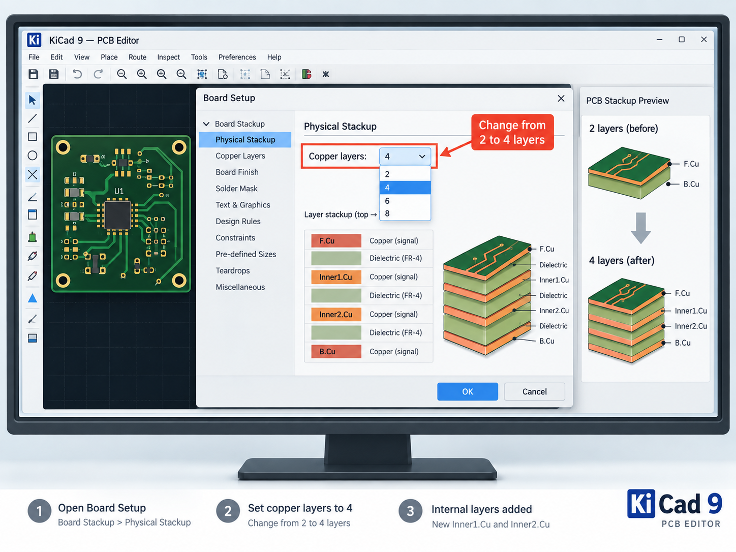
To add a new copper layer to KiCad 9, open PCB Editor → File → Board Setup → Board Stackup → Physical Stackup, then increase the copper layer count. For example, changing a two-layer PCB to four layers adds the internal copper layers In1.Cu and In2.Cu.

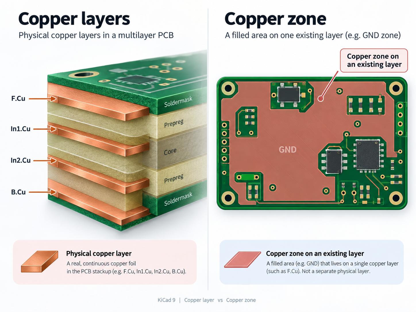
Adding a copper layer is different from adding a copper zone. A copper layer changes the physical PCB stackup. A copper zone places copper on an existing layer for ground, power, shielding, or current distribution. Knowing which one you need avoids unnecessary setup changes.
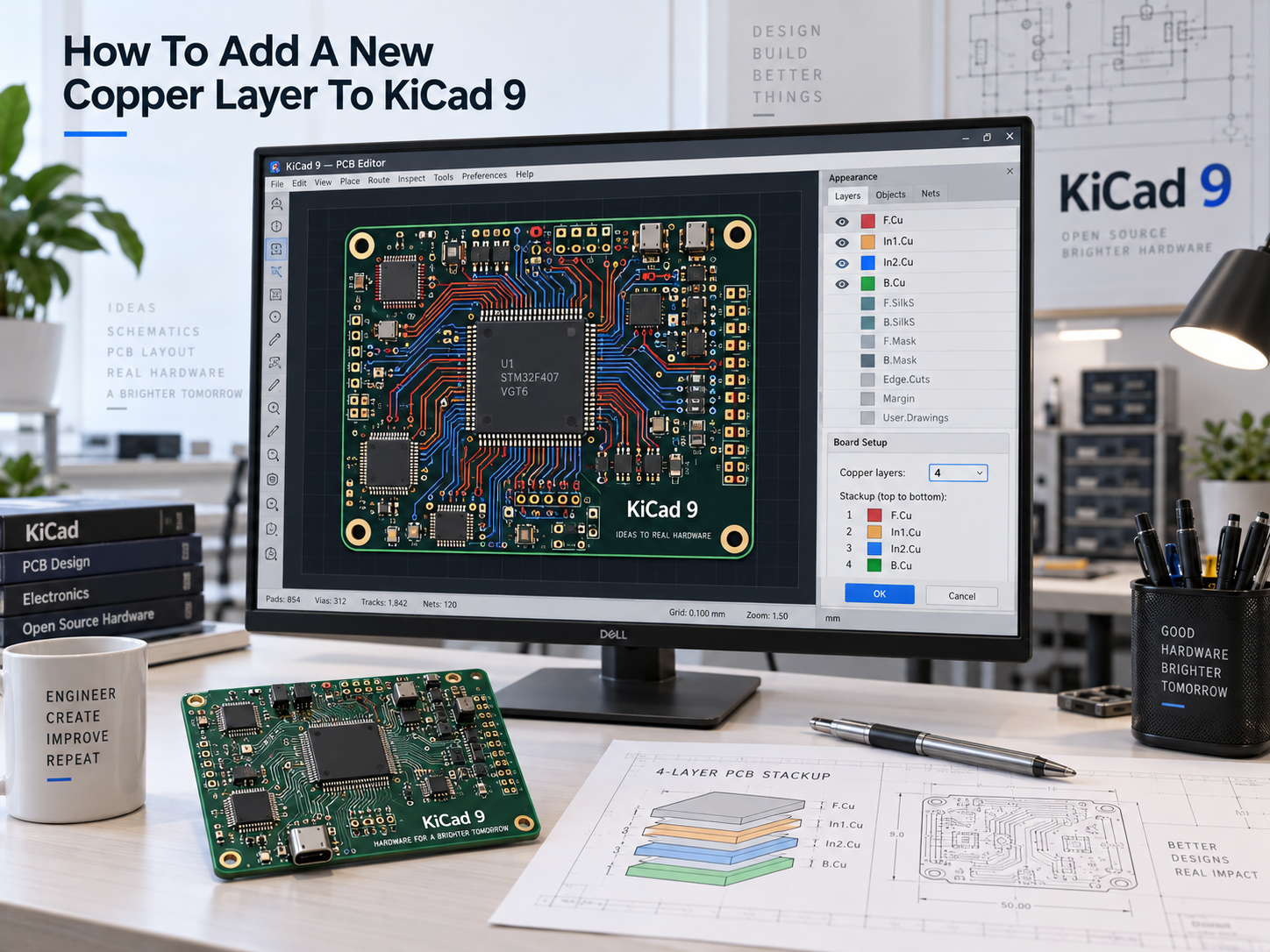
How to add a new copper layer to KiCad 9 in a four-layer PCB design

How to Add a New Copper Layer to KiCad 9?

To add copper layers in KiCad 9, change the layer count in Physical Stackup.

  1. Open the PCB layout in PCB Editor.
  2. Go to File → Board Setup.
  3. Select Board Stackup → Physical Stackup.
  4. Find the Copper layers setting.
  5. Change the board from 2 layers to 4 layers, or select another supported layer count.
  6. Review the new internal copper layers.
  7. Click OK.
KiCad 9 Physical Stackup changing a PCB from two copper layers to four copper layers

A standard four-layer board will normally include:

  • F.Cu
  • In1.Cu
  • In2.Cu
  • B.Cu

KiCad 9 uses an even number of physical copper layers, so a two-layer design normally moves to four layers rather than three.

After increasing the layer count, check the stackup values instead of treating them as placeholders. Useful items to review include:

  • Copper thickness
  • Dielectric thickness
  • Overall board thickness
  • Layer order
  • Material type

Do not use Add User Defined Layer to create another electrical copper layer. User-defined layers are intended for drawings, notes, fabrication information, or other non-routing content.

Copper Layer vs Copper Zone in KiCad 9: What Is the Difference?

A copper layer is a physical conductive layer in the PCB, while a copper zone is an area of copper created on an existing layer.

Item Copper Layer Copper Zone
Main purpose Adds a physical PCB layer Adds copper within an existing layer
Examples F.Cu, In1.Cu, In2.Cu, B.Cu GND pour, power plane
Setup location Physical Stackup Add Filled Zone
Changes PCB layer count Yes No
Assigned to a net Not by itself Usually yes
Comparison between physical copper layers and a copper zone in KiCad 9

For example, adding In1.Cu gives the PCB another physical copper layer. It does not automatically turn that layer into a ground plane.

If you want In1.Cu to work as ground, create a copper zone on that layer and assign it to the GND net.

This distinction matters because many searches for “how to add copper layer in KiCad” actually come from users who only need a ground or power pour.

How to Add a Ground Plane in KiCad 9?

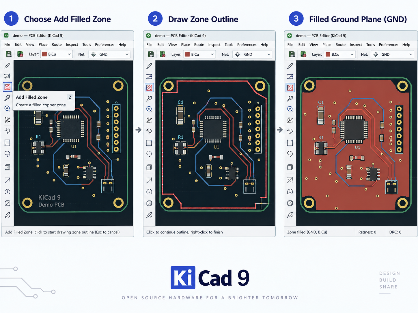
To add a ground plane in KiCad 9, create a filled copper zone and assign it to the GND net.

  1. Select the copper layer where the plane should be created.
  2. Click Add Filled Zone.
  3. Click inside the PCB outline.
  4. Select the GND net.
  5. Confirm the target copper layer.
  6. Draw the zone boundary around the required area.
  7. Finish the outline.
  8. Press B to refill all zones.
How to add a GND filled copper zone and ground plane in KiCad 9

On a two-layer PCB, a GND zone is often placed on B.Cu. On a four-layer board, an internal layer such as In1.Cu may be used as a more continuous ground reference.

The zone boundary only defines where KiCad is allowed to calculate copper. The actual filled shape depends on traces, vias, pads, clearances, cutouts, and design rules. After routing changes, press B again so the copper fill reflects the latest layout.

Which KiCad Copper Zone Properties Should You Set?

The most important KiCad copper zone properties are the net, layer, clearance, minimum width, pad connection, and thermal relief settings.

  • Layer: Sets where the zone is placed.
  • Net: Connects the zone to GND, power, or another net.
  • Clearance: Controls spacing from copper on other nets.
  • Minimum width: Removes copper areas that become too narrow.
  • Pad connections: Sets solid, thermal relief, or no connection.
  • Thermal relief gap: Defines spacing around thermally connected pads.
  • Thermal spoke width: Sets the width of each thermal connection.
  • Fill style: Selects solid or hatched copper.
  • Island removal: Controls how disconnected copper islands are handled.

The values should match both the electrical requirement and the PCB manufacturer’s design rules. Clearance and minimum width deserve particular attention because they can directly change the final filled geometry.

Thermal relief settings also affect assembly. A large solid copper plane can pull heat away from a pad during soldering, while thermal spokes reduce that heat transfer.

How Does KiCad Zone Priority Work?

KiCad zone priority controls which overlapping copper zone is filled first.

A higher-priority zone is calculated before a lower-priority zone. The lower-priority zone then keeps the required clearance from the copper already created.

A common example is:

  • A large GND zone across most of the layer
  • A smaller +5V zone inside part of the same area

If the +5V area must remain inside the larger ground region, the power zone can be given a higher priority.
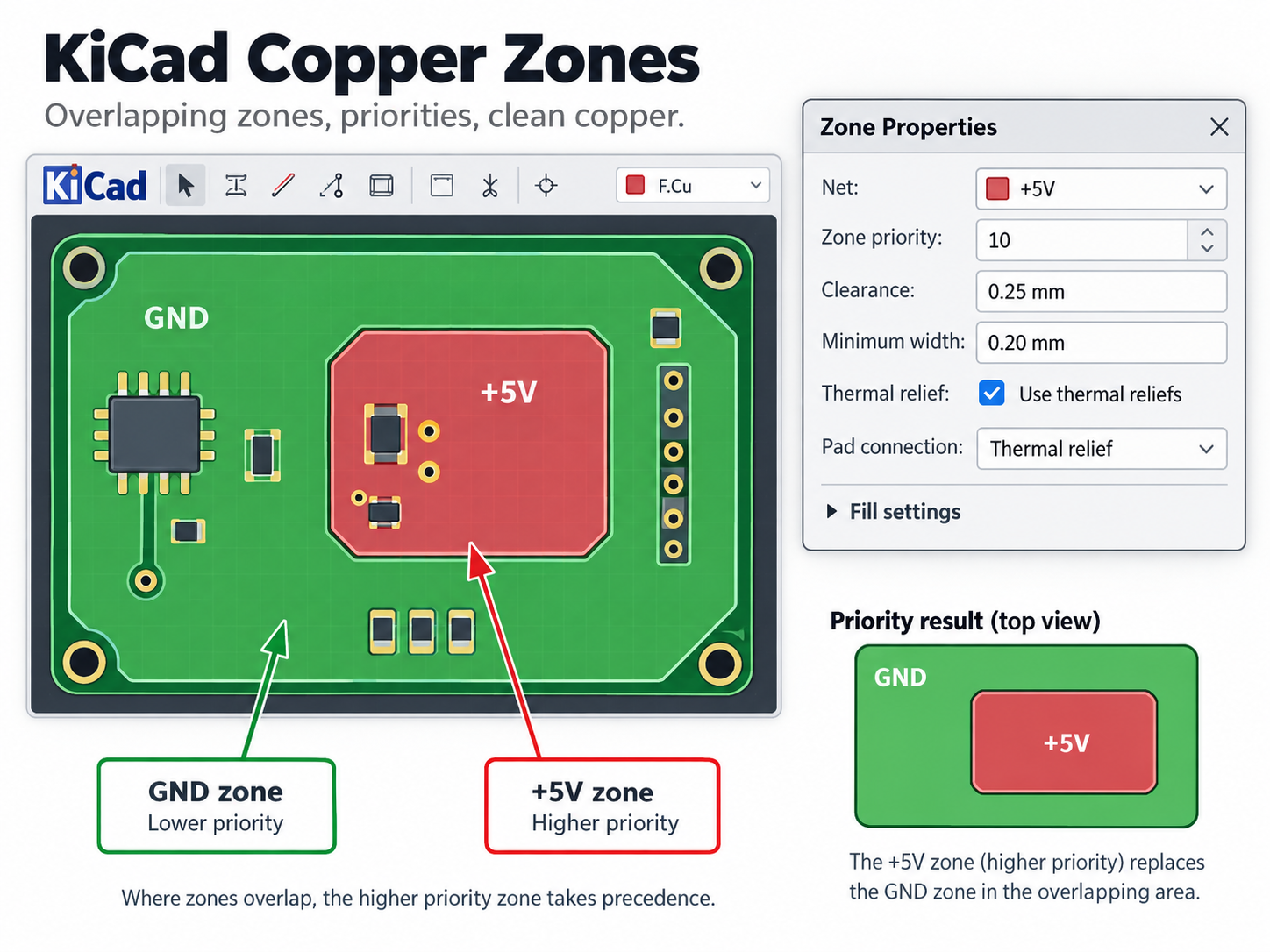
KiCad copper zone properties and zone priority for overlapping GND and 5V zones

Zone priority is useful when two or more copper zones intentionally overlap. It is not a fix for an incorrect net, poor outline, or unsuitable clearance setting.

If overlapping zones behave unexpectedly, check:

  • Net assignment
  • Target layer
  • Zone outline
  • Clearance
  • Priority value

For layouts with several zones, the Zone Manager makes it easier to compare their settings in one place.

Why Is the KiCad Ground Plane Not Filling?

If a KiCad ground plane is not filling, press B first to refill all zones.

If the problem remains, check:

  • Wrong net: Confirm that the zone is assigned to GND.
  • Wrong layer: Make sure the zone is on the copper layer you are viewing.
  • Incomplete outline: Check that the zone boundary is closed.
  • Large clearance: Too much spacing can remove copper from narrow areas.
  • Large minimum width: Narrow copper sections may be discarded.
  • Keepout or rule area: These may block copper from filling.
  • Board cutout: Copper will not fill through cutouts or outside the board edge.
  • Island removal: Small disconnected copper areas may be removed automatically.
  • Hidden fill display: The zone may be filled but only its boundary is visible.

If only one section of the plane is missing, inspect that local area closely. Dense vias, BGA fanout, narrow board sections, or nearby keepouts often create the problem. After making changes, refill the zones and run DRC again.

How to Hide Filled Zones in KiCad Without Deleting Them?

To hide filled zones in KiCad, switch the PCB Editor to show only the zone boundaries.

This changes the display only. It does not remove the copper zone from the design.

  • Hide zone fill: Keeps the zone but hides the rendered copper.
  • Unfill zone: Removes the calculated fill until it is filled again.
  • Delete zone: Removes the zone object completely.

Hiding the fill is useful when large power or ground areas make routing difficult to see. If a copper zone suddenly appears to be missing but its outline is still visible, check the display mode before changing the design.

What Should You Check Before Fabricating a Multilayer KiCad PCB?

Before fabricating a multilayer KiCad PCB, confirm that the KiCad stackup matches a stackup your PCB manufacturer can actually build.
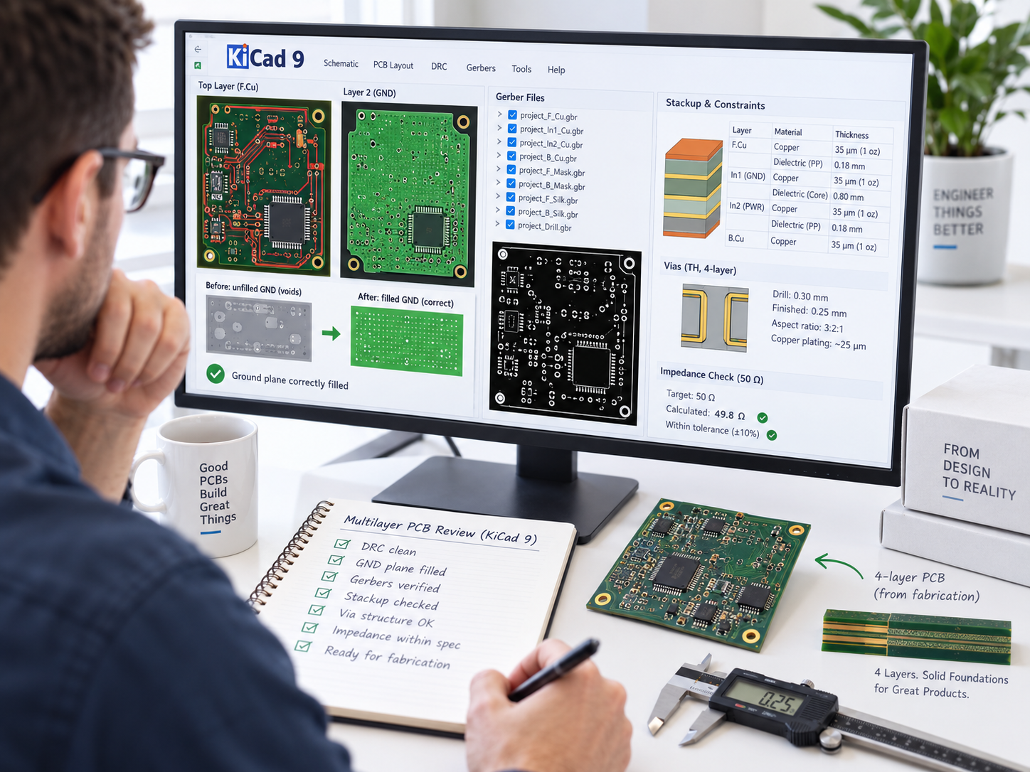
KiCad 9 multilayer PCB fabrication review with Gerber stackup via and impedance checks

Check these items before releasing fabrication data:

  • Copper layer count: Make sure all intended layers are included.
  • Layer order: Confirm the correct position of signal, ground, and power layers.
  • Board thickness: Verify the finished PCB thickness.
  • Copper thickness: Confirm outer- and inner-layer copper requirements.
  • Dielectric structure: Review core and prepreg thicknesses.
  • Controlled impedance: Confirm material, dielectric thickness, copper thickness, and target impedance.
  • Via structure: Check through holes, blind vias, buried vias, or microvias.
  • Plane continuity: Look for fragmented ground or power planes.
  • Zone fill: Press B before final output.
  • DRC: Resolve relevant clearance and connectivity errors.
  • Gerber and drill data: Confirm that every copper and drill layer is exported correctly.

A four-layer board created in KiCad is not automatically a production-ready four-layer stackup. The PCB factory may use different prepreg thicknesses, core materials, or copper weights from the default CAD values.

For controlled-impedance boards, confirm the production stackup before finalizing critical trace widths. A dielectric change can alter the impedance even when the routing geometry stays the same.

If your KiCad design is ready for fabrication, EBest Circuit can review the Gerber files, stackup, material selection, copper weight, via structure, and impedance requirements before production.

For schematic net naming, see our guide to how to make labels in KiCad.

FAQ About Adding Copper Layers in KiCad 9

1. Can I add only one new copper layer in KiCad 9?
No. KiCad 9 uses an even number of physical copper layers, so a two-layer PCB normally changes to four layers rather than three.

2. How do I change a KiCad PCB from 2 layers to 4 layers?
Open PCB Editor → File → Board Setup → Board Stackup → Physical Stackup, then change the copper layer count from 2 to 4.

3. Is In1.Cu automatically a ground plane in KiCad?
No. In1.Cu is only an internal copper layer. Create a copper zone on it and assign that zone to GND if you want to use it as a ground plane.

4. What is the shortcut to refill copper zones in KiCad?
Press B to refill all copper zones.

5. Why did my copper fill disappear in KiCad?
The fill may be hidden, unfilled, blocked by clearance rules, or removed by zone settings. Check the display mode first, then refill the zone with B.

6. Can one copper zone be used on multiple layers in KiCad 9?
Yes. A zone can be assigned to multiple copper layers while using the same net, with the copper fill calculated separately on each selected layer.

Adding a new copper layer in KiCad 9 is simple once you use the correct stackup settings. The more important step is making sure the final layer structure, zones, vias, and fabrication data match the PCB you actually want to manufacture.


For PCB fabrication or PCBA support, send your Gerber files, stackup requirements, material requirements, copper weight, impedance targets, and quantity to sales@bestpcbs.com for DFM review.

You may also like

Thick PCB Board vs Heavy Copper PCB: Design and Selection Guide

September 10th, 2026

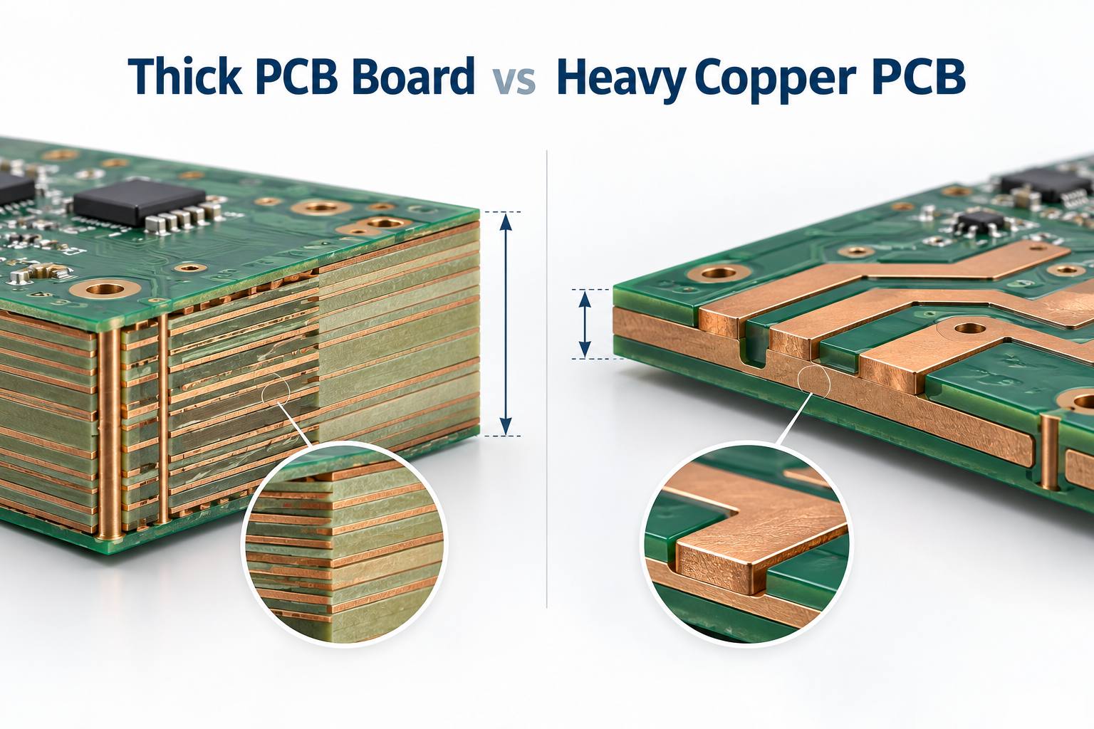
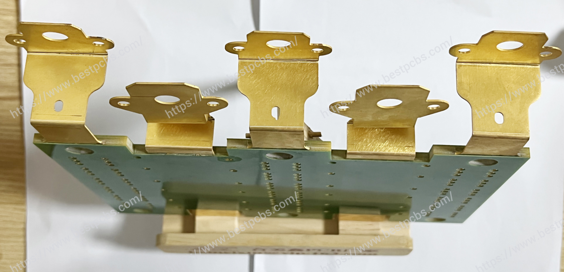
A thick pcb board and a heavy copper PCB solve different engineering problems. The first increases the total finished thickness of the board; the second increases the copper thickness on selected or all conductive layers. A board can be mechanically thick without carrying high current, and a heavy copper design can fit inside a conventional overall thickness.

This distinction affects stackup planning, hole sizes, impedance, thermal behavior, connector fit, manufacturing cost, and the information a fabricator needs before quotation. This guide compares the two constructions so engineers and buyers can specify the right one instead of treating “thick board” and “thick copper” as interchangeable terms.

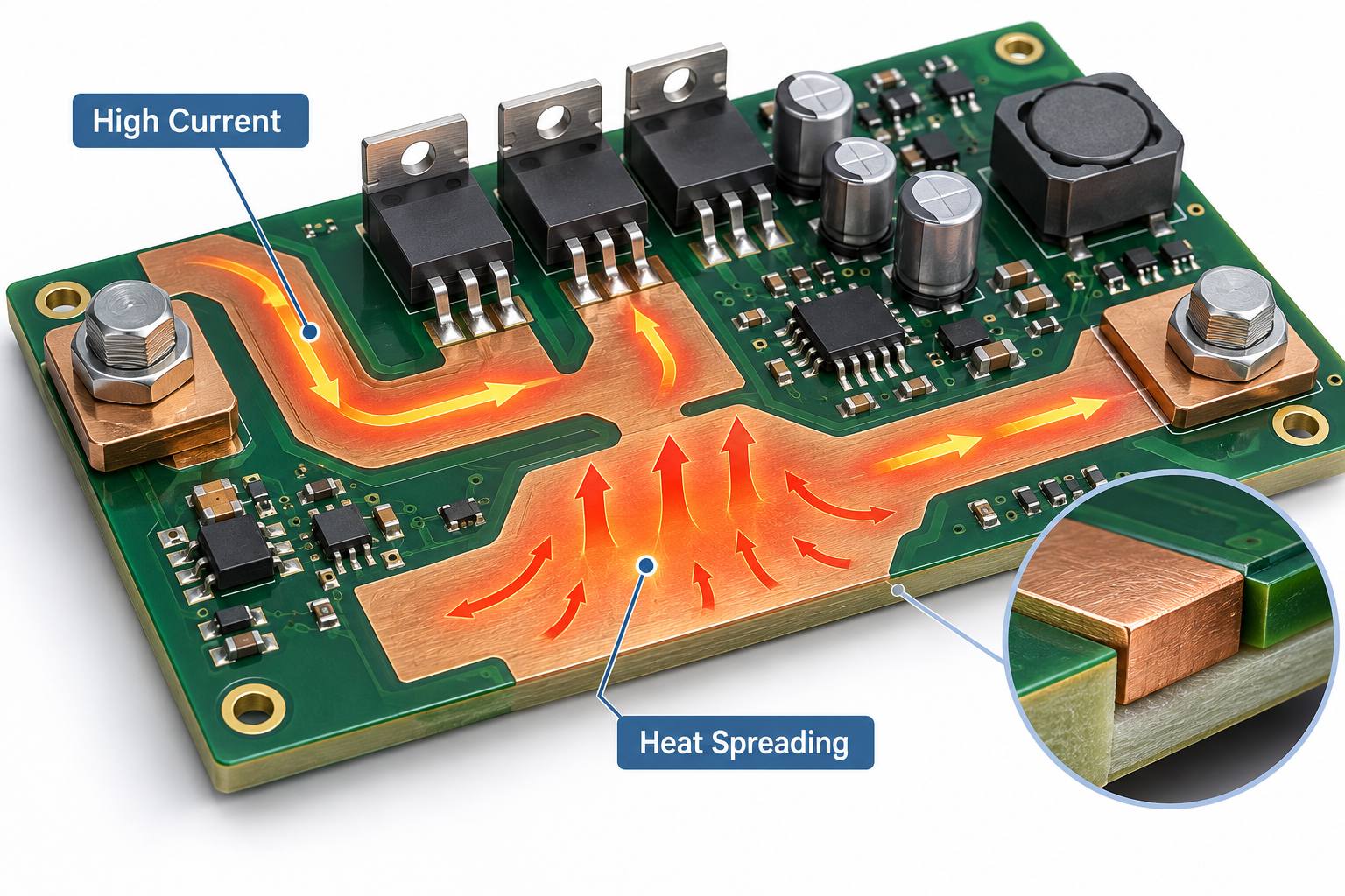
Thick PCB board versus heavy copper PCB engineering comparison

What Is a Thick PCB Board?

A thick PCB board is a rigid printed circuit board whose total finished thickness is greater than the common construction used for a similar product. The measurement spans the complete board from one outer surface to the other. It includes cores, cured prepregs, copper layers, plating, solder mask, and smaller finish contributions.

The term describes a mechanical dimension, not a specific copper weight. Designers may choose a thicker construction to:

  • Increase stiffness across a large unsupported area.
  • Support transformers, relays, power modules, large connectors, or other heavy components.
  • Meet card-edge, press-fit, guide-rail, enclosure, or mounting requirements.
  • Fit additional routing and reference-plane layers into a multilayer stackup.
  • Provide required dielectric spacing between conductors.
  • Control bending in equipment exposed to vibration or mechanical handling.

A thick board should not be selected only because it appears stronger. Extra thickness can create higher hole aspect ratios, longer routing cycles, different depaneling limits, more material usage, and tighter connector-fit constraints.

How Thick Is a PCB Board?

The practical answer to “how thick is a pcb board” depends on the application and the complete stackup. Many rigid FR-4 boards use a finished thickness near 1.6 mm, while thinner products may use 0.8, 1.0, or 1.2 mm. Mechanically demanding or high-layer-count designs may use 2.0, 2.4, 3.2 mm, or another project-specific value.

These numbers are not automatic manufacturing categories. A 2.4 mm two-layer board with generous holes is usually less demanding than a 2.4 mm multilayer board with small plated holes, controlled impedance, heavy outer copper, and a strict finished-thickness tolerance. The fabricator must review the thickness together with:

  • Layer count and copper distribution.
  • Core and prepreg constructions.
  • Smallest drilled and finished hole sizes.
  • Plated-through, blind, buried, or filled via structures.
  • Controlled-impedance geometries.
  • Board dimensions, panelization, and routing method.
  • Connector, press-fit, and enclosure tolerances.

For a broader dimensional reference, see our guide to standard printed circuit board thickness.

What Is the Standard PCB Thickness?

The question “what is the standard pcb thickness” usually refers to 1.6 mm, approximately 0.062 inch. It is a widely used rigid-board value because common laminate constructions, connectors, housings, fixtures, and assembly processes are often designed around it. However, 1.6 mm is a common default rather than a universal rule.

Finished thickness is built from real laminate and prepreg options. Prepreg does not behave like a fixed spacer: its pressed thickness changes with glass style, resin content, copper pattern density, resin flow, and the lamination cycle. Material suppliers such as Isola publish laminate and prepreg construction data that fabricators use when developing manufacturable stackups.

If a mechanical drawing calls out only an unusual finished thickness but does not define the stackup, the designer should let the PCB manufacturer propose available core and prepreg combinations. This is safer than forcing a theoretical build that depends on unavailable materials or unrealistic pressed thicknesses.

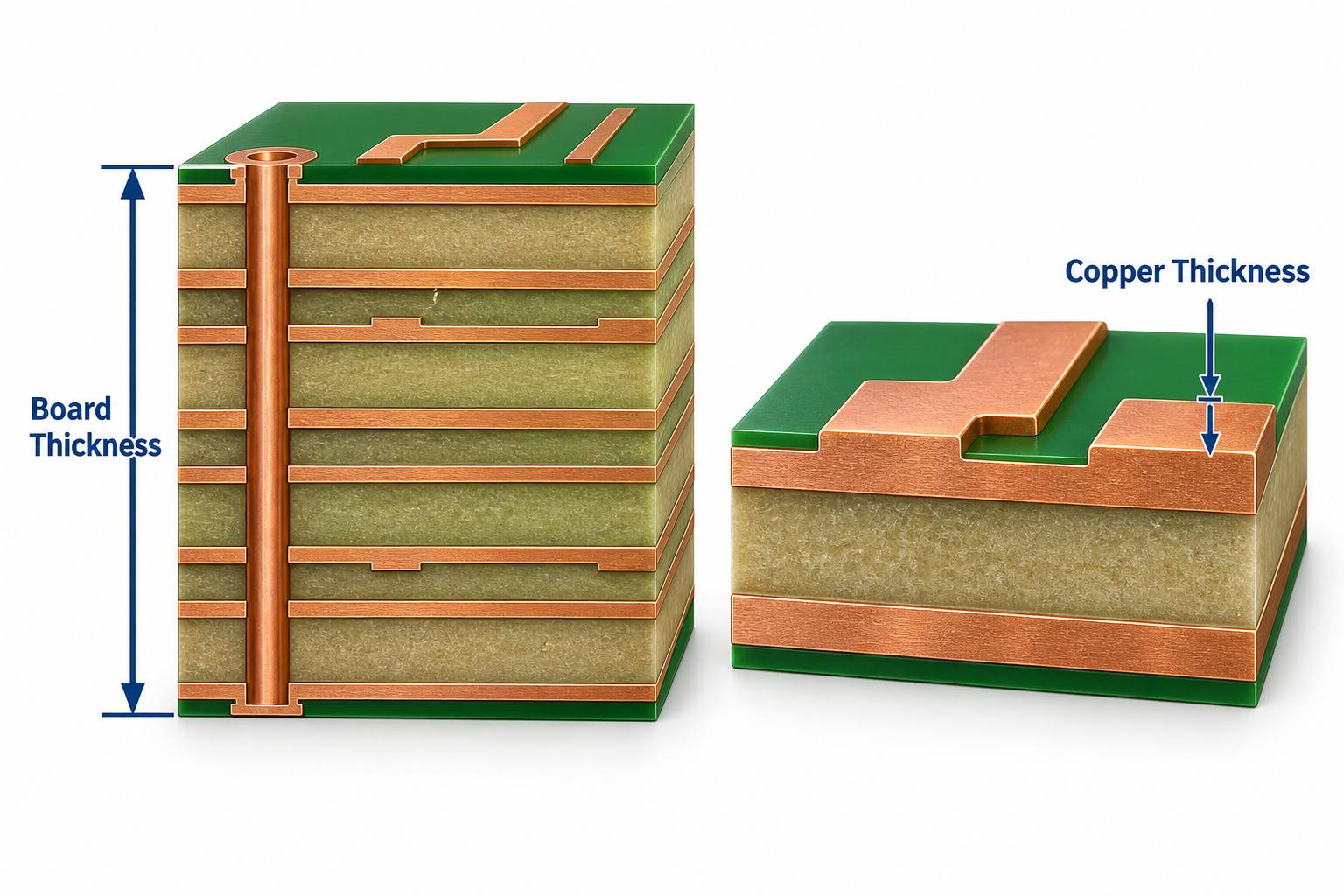
PCB board thickness compared with copper thickness in cross-section

Thick PCB Board vs Heavy Copper PCB: What Is the Difference?

The shortest distinction is simple: board thickness is a mechanical stack dimension, while copper thickness is a conductor dimension. They influence different parts of PCB performance and manufacturing.

Comparison Thick PCB Board Heavy Copper PCB
Primary definition Greater total finished board thickness Greater copper thickness or copper weight on one or more layers
Main purpose Mechanical stiffness, stackup space, connector fit, or dielectric spacing High-current conduction, lower conductor resistance, heat spreading, or robust power connections
Most affected design data Stackup, hole size, aspect ratio, impedance, enclosure, routing, and tolerance Trace width and spacing, pad geometry, etching, resin fill, plating, current rise, and thermal path
Typical manufacturing concern Deep drilling, hole preparation, plating coverage, lamination, routing, and warpage control Etch compensation, copper balance, resin filling around tall conductors, conductor definition, and thermal mass
Can it exist without the other? Yes. A thick board can use standard copper. Yes. A heavy copper board can retain a conventional finished thickness.

For example, a 3.2 mm FR-4 board with 1 oz copper is mechanically thick but is not a heavy copper PCB. A 1.6 mm board with 4 oz copper is a heavy copper design even though its total thickness is conventional. Some power products need both: a thick structure for stiffness and thick copper for electrical and thermal performance.

How Does a Thick Board Change Stackup and Impedance?

Increasing total board thickness changes the dielectric distance available between copper layers. If trace width, copper thickness, and dielectric properties remain unchanged, a larger trace-to-reference-plane distance changes characteristic impedance. Therefore, a designer cannot simply stretch every dielectric layer to reach a new finished thickness and expect the same controlled-impedance result.

A practical thick-board stackup review covers:

  • Reference-plane location: High-speed signals still need a nearby and continuous return plane.
  • Dielectric selection: Core and prepreg choices must match available material constructions and the required pressed thickness.
  • Copper balance: Symmetric copper and dielectric distribution helps reduce lamination stress and bow or twist.
  • Resin filling: Heavy copper or uneven pattern density may require higher-resin prepreg to fill around conductors.
  • Finished tolerance: The stackup must leave a realistic process window for material and lamination variation.

Do not approve the mechanical thickness independently from impedance. Send the impedance table, target values, referenced layers, and any material restrictions with the stackup so the fabricator can model the construction as one system.

How Do Drilling and Plating Limits Change?

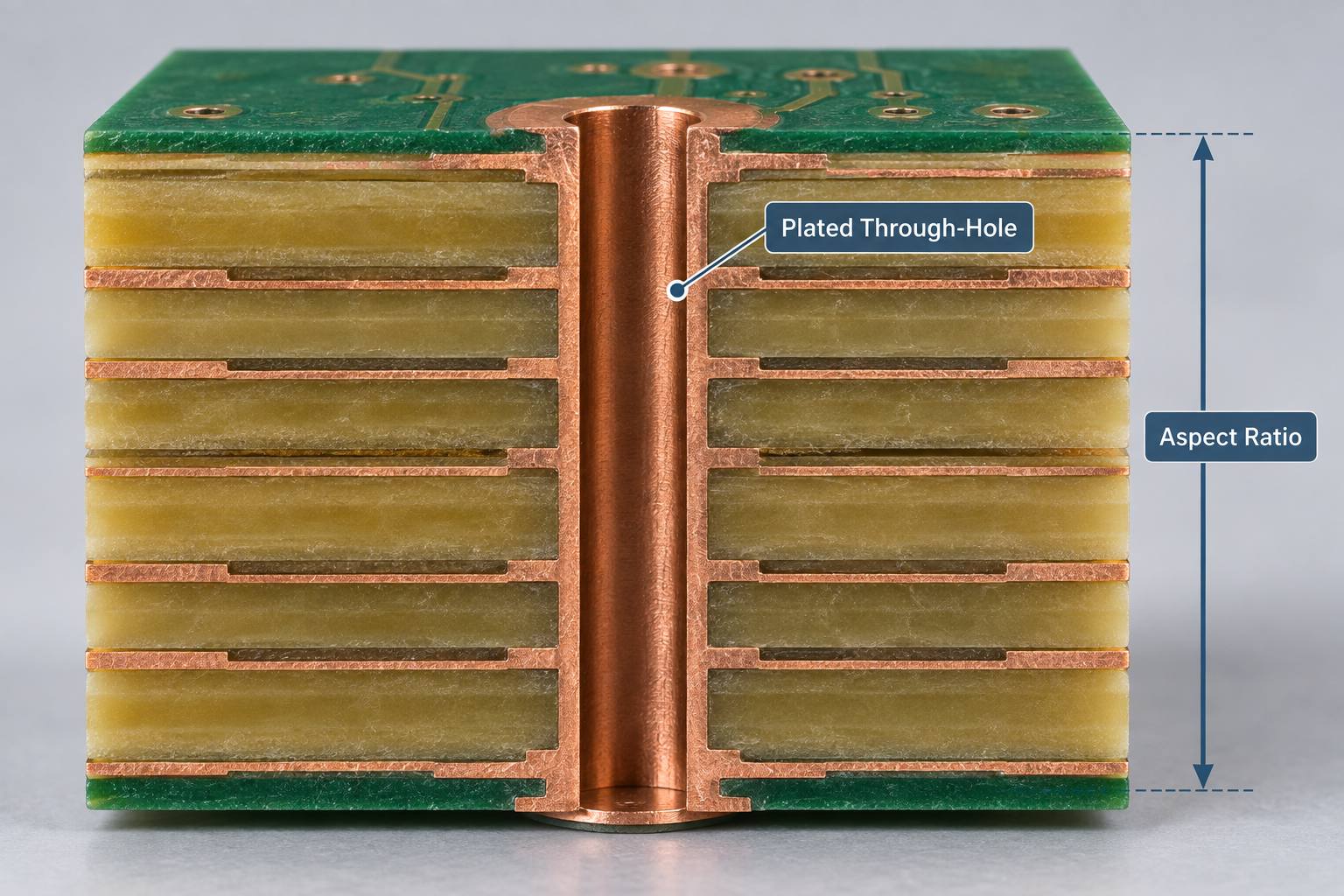
As a board becomes thicker, a mechanically drilled hole becomes deeper. If the drill diameter stays small, the hole aspect ratio rises. This makes debris removal, desmear, activation, and copper deposition inside the barrel more demanding. The result can be thin plating in the center of the hole, barrel voids, poor registration margin, or lower thermal-cycling reliability.

Aspect ratio is commonly expressed as board thickness divided by drilled hole diameter. It is a DFM relationship, not a target that should be pushed without considering the material, layer count, plating process, copper requirement, and acceptance class. A thicker finished board may need one or more of the following changes:

  • Increase the mechanically drilled hole diameter.
  • Use staged or controlled drilling conditions.
  • Adjust the via structure instead of using one deep through-hole.
  • Increase annular-ring and registration allowance where required.
  • Specify hole-wall copper and microsection acceptance clearly.
  • Review press-fit hole tolerances and final plating buildup.
Thick PCB plated through-hole and drilling aspect ratio

IPC-6012F establishes qualification and performance requirements for rigid printed boards, including multilayer constructions with plated-through, blind, buried, and microvia structures. The applicable class, customer drawing, procurement specification, and agreed deviations should be defined before production.

Heavy Copper PCB Design: What Must Be Reviewed?

Heavy copper PCB design starts with electrical and thermal requirements, not with a higher copper weight chosen by habit. A thicker conductor can reduce resistance and support more current, but the result also depends on trace width, conductor location, ambient conditions, allowed temperature rise, adjacent copper, airflow, duty cycle, terminal design, and heat-transfer paths.

IPC-2152 provides guidance on the relationship between current, conductor dimensions, and acceptable temperature rise. It is a better basis for conductor sizing than assuming that a mechanically thicker board will automatically carry more current.

Manufacturing review should include:

  • Copper weight required on every inner and outer layer.
  • Minimum line width and spacing after etch compensation.
  • Pad, via, and neck-down geometry at high-current transitions.
  • Resin filling around tall copper features.
  • Copper balance across the panel and stackup.
  • Thermal reliefs, solderability, and assembly heat demand.
  • Finished copper and plated-hole copper acceptance.
Heavy copper PCB design for high current and heat spreading

EBest Circuit supports heavy copper PCB projects for power distribution, heat spreading, planar transformers, power converters, and related high-current applications. Exact copper, spacing, stackup, and test requirements must be confirmed against the production data.

Which Construction Should You Choose?

Choose the construction from the problem you are trying to solve. Mechanical stiffness does not replace electrical conductor sizing, and additional copper does not guarantee connector fit or board rigidity.

Primary Requirement Review First Likely Direction
Large board or heavy components need more rigidity Board dimensions, mounting points, vibration, and enclosure support Thicker finished board
High current with an acceptable temperature rise Current, trace width, copper weight, duty cycle, and cooling Heavy copper PCB
More routing and reference planes Layer count, impedance, dielectric spacing, and via structure Thicker multilayer stackup, if required
High current plus mechanical stiffness All electrical, thermal, stackup, drilling, and enclosure constraints Combined thick-board and heavy-copper construction
Connector or card-edge fit Specified finished thickness and tolerance at the mating interface Board thickness driven by connector geometry

If the design needs both thickness and heavy copper, review them together before layout release. Thick copper consumes vertical space, changes resin demand, restricts fine features, and can alter the final thickness. A late copper-weight change can therefore invalidate the stackup and controlled-impedance calculations.

What Should You Send for a Manufacturing Review?

A useful DFM package lets the fabricator evaluate the mechanical and conductor requirements separately, then confirm how they interact. Include:

  • Gerber or ODB++ fabrication data and drill files.
  • Layer count and proposed stackup.
  • Target finished board thickness and tolerance.
  • Base material, Tg, CTI, thermal, or high-frequency requirements.
  • Copper weight for every layer and any selective heavy-copper areas.
  • Smallest drilled hole, smallest finished hole, via types, and filled-via requirements.
  • Controlled-impedance values and referenced layer pairs.
  • Board dimensions, panel or delivery format, outline tolerance, and connector requirements.
  • Surface finish, solder mask, legend, electrical test, acceptance class, and required reports.
  • Prototype and production quantities plus the required delivery date.

If the project is already defined as a thick mechanical build, our thick PCB board manufacturing guide explains the detailed stackup and quotation review path.

FAQ About Thick PCB Boards and Heavy Copper PCBs

Is a 2.0 mm PCB considered thick?

It is thicker than the common 1.6 mm construction, but whether it needs special processing depends on its layer count, material, dimensions, holes, copper weight, tolerances, and routing method.

Does a thick PCB carry more current?

Not automatically. Current capacity is primarily determined by conductor geometry, temperature-rise limits, copper environment, cooling, and operating conditions. Overall board thickness is a separate mechanical property.

Can a heavy copper PCB be only 1.6 mm thick?

Yes. A fabricator may build heavy copper into a conventional finished thickness if the layer structure, dielectric spacing, resin fill, feature sizes, and tolerance can be manufactured reliably.

Why are small vias difficult in a thick board?

The deeper hole creates a higher aspect ratio. Hole cleaning and uniform copper deposition become more demanding, especially when the finished hole is small or the specified barrel copper is high.

Should I specify copper in ounces or micrometers?

Either can be used if the procurement documents are consistent, but clearly distinguish base copper from finished copper after plating. State the requirement for each layer rather than using one value for the entire PCB.

Can board thickness be changed after impedance routing is complete?

Only after the impedance geometry is recalculated. Changing the dielectric distance to the reference plane can change impedance, so the fabricator must review the revised stackup, trace width, spacing, copper thickness, and material properties.

How Can EBest Circuit Support Your PCB Project?

EBest Circuit reviews thick-board and heavy-copper requirements as two connected but distinct engineering inputs.

Send your Gerber or ODB++ data, stackup, finished thickness, copper weight by layer, drill table, impedance requirements, material notes, surface finish, test standard, quantity, and delivery target to sales@bestpcbs.com. We will review the manufacturable construction before quotation and prototype release.

You may also like

What Is a BCM? Inside a Vehicle Body Control Module

September 10th, 2026

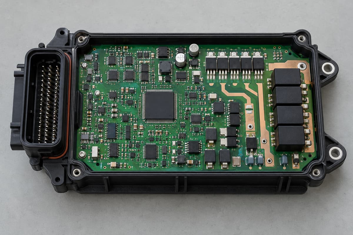
BCM most often means Body Control Module in an automotive context. It is an electronic control unit that reads switches, sensors, and vehicle-network messages, runs body-control logic, and drives loads such as lamps, door locks, windows, mirrors, wipers, and interior convenience systems.

A BCM is not just a processor board. Its PCB must place low-voltage logic, vehicle communications, protected power inputs, and higher-current load drivers in one compact assembly while handling electrical transients, heat, electromagnetic interference, vibration, and long service life. This guide opens the module and follows the signal path from an input to a physical vehicle function.

What Is a BCM hero showing a body control module PCB inside a vehicle

What Is a BCM on a Car?

A BCM on a car is the electronic control unit responsible for body and convenience functions rather than combustion, traction, or transmission control. The exact boundary varies by vehicle: one platform may use a central BCM, while another divides the same work among front, rear, door, or zone controllers.

The search phrase what is a bcm module usually refers to the same device. “Module” describes the complete unit: the populated PCB, connector interface, housing, firmware, and calibration data. Replacing only the circuit board may not restore operation if the vehicle also requires coding, key matching, or configuration.

Module Primary responsibility Typical inputs and outputs
BCM Body, access, lighting, and cabin convenience functions Door switches, locks, lamps, windows, mirrors, wipers, network messages
ECM Engine operation Engine sensors, fuel injection, ignition, emissions actuators
PCM Powertrain control; on some vehicles it combines engine and transmission control Engine and transmission sensors, injectors, ignition, shift control

BCM, ECM, and PCM names are not perfectly standardized across automakers. The vehicle service information and electrical architecture remain the authority for a specific model.

What Does a BCM Control in a Car?

A BCM commonly controls exterior and interior lights, central locking, power windows, mirrors, wipers, washers, retained accessory power, and selected heaters or motors. It also coordinates these functions with door modules, gateways, and other ECUs when the vehicle architecture distributes the load control.

  • Exterior lighting: headlamps, daytime running lamps, turn indicators, brake lamps, and welcome-light sequences.
  • Access: central locking, keyless-entry requests, trunk or tailgate release, and anti-theft status exchange.
  • Doors and glass: window motors, mirror fold or heating, door-ajar inputs, and child-lock functions.
  • Wipers and washers: stalk requests, intermittent timing, rain-sensor messages, and pump or motor control.
  • Cabin functions: interior lamps, retained accessory power, seat or steering-wheel heaters, and wake/sleep coordination.

Not every vehicle assigns every function to the BCM. Some loads are driven by door or zone modules after receiving BCM commands over CAN or LIN; the model-specific wiring diagram identifies the responsible controller and output stage.

How Does a BCM Work?

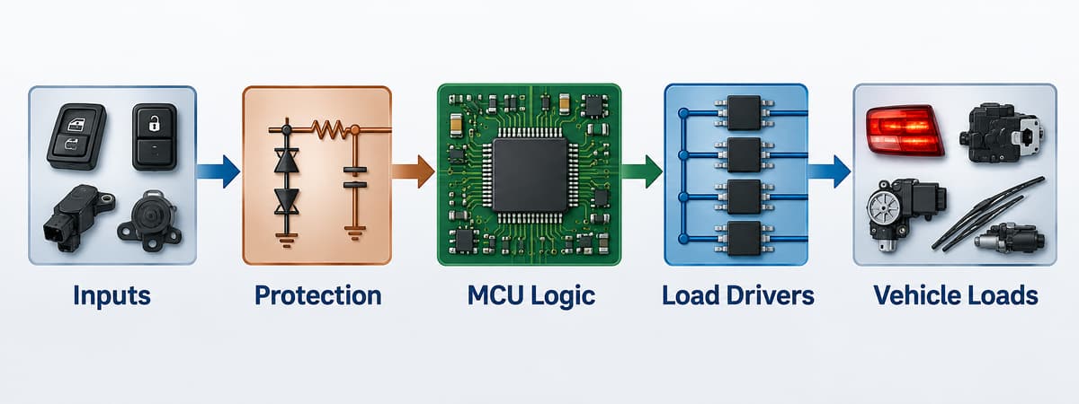
A BCM works through five blocks: it receives an input, protects and conditions the signal, evaluates the request in a microcontroller, commands a driver, and monitors the resulting load. For example, a door-switch transition can be debounced by the input circuit, interpreted by firmware, transmitted to another ECU if required, and used to switch a courtesy lamp through a protected high-side output.

BCM signal flow from inputs through protection and MCU logic to load drivers and vehicle loads

The complete path normally includes:

  1. Input acquisition: switches, Hall sensors, analog sensors, and messages from CAN or LIN nodes.
  2. Protection and conditioning: filtering, voltage clamping, reverse-polarity protection, level shifting, and transient-tolerant interfaces.
  3. Decision logic: an MCU applies timing, state-machine, safety, diagnostic, and energy-management rules.
  4. Load actuation: smart high-side switches, low-side drivers, half bridges, full bridges, or relays operate lamps, heaters, solenoids, and motors.
  5. Feedback: current sense, fault flags, temperature status, position signals, and bus messages confirm whether the command succeeded.

Sleep behavior is another core function. When the vehicle is parked, the BCM must reduce its own current and coordinate network sleep without missing legitimate wake events such as a key request or door opening.

What Is Inside a BCM Module?

Inside a BCM module are a microcontroller, regulated power rails, CAN or LIN transceivers, protected input circuits, load drivers, nonvolatile memory, clocks, connectors, and thermal paths. Exact parts depend on the vehicle architecture, but real automotive reference designs make the functional split concrete.

Opened automotive body control module showing the internal PCB, connectors, MCU, transceivers, and power drivers
Circuit function Representative automotive device Role in a BCM-class design
Microcontroller TI AM263P4-Q1 Runs control logic, diagnostics, timing, and network software in a recent zone-controller reference design
Power-management IC TI TPS65386x-Q1 family Generates and supervises regulated rails for the processor and peripheral circuits
CAN/CAN FD transceiver TI TCAN1043A-Q1 Converts MCU logic-level data to the differential vehicle bus and supports wake/sleep behavior
LIN transceiver TI TLIN1021A-Q1 Connects lower-cost local nodes such as switches, small actuators, or door electronics
Smart high-side switch TI TPS1HC30-Q1 Switches a protected body load and provides diagnostic feedback
Motor driver TI DRV8245S-Q1 Controls bidirectional DC loads such as selected window, latch, or seat mechanisms

These are examples, not a universal BCM bill of materials. A more integrated approach is also possible: Infineon’s TLE9560-3QX system basis chip combines a 5 V regulator, CAN FD and LIN communication, two half-bridge drivers, high-side outputs, and SPI control in one device. The final choice depends on current, channel count, diagnostic coverage, thermal limits, software architecture, and the automaker’s component requirements.

How Does a BCM Communicate With Other ECUs?

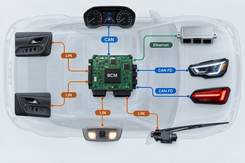
A BCM communicates with other ECUs through vehicle networks, most commonly CAN or CAN FD for coordinated control and LIN for lower-cost local devices. Some newer centralized or zonal architectures also use automotive Ethernet for higher-bandwidth links, but not every BCM includes every interface.

Vehicle network diagram connecting a BCM to body functions through CAN, CAN FD, LIN, and Ethernet
  • CAN: robust multi-node communication for status, commands, diagnostics, and coordination among body, gateway, powertrain, and instrument modules.
  • CAN FD: retains CAN arbitration while allowing a larger payload and faster data phase when the network and transceivers support it.
  • LIN: a lower-cost single-master network suited to local switches, small motors, lighting nodes, and door electronics.
  • Automotive Ethernet: a higher-bandwidth link increasingly associated with gateways and zone controllers rather than a universal requirement for conventional BCMs.

The PCB must keep these communication paths away from noisy switching nodes, preserve their return paths, and implement the termination, common-mode filtering, ESD protection, and connector pinout required by the actual interface design.

What Makes a BCM PCB Different From a General Control Board?

A BCM PCB differs from a general control board because it combines battery-connected power, sensitive digital logic, network interfaces, and multiple switched loads in a harsh electrical and mechanical environment. A circuit that works on a bench can still fail in a vehicle if the layout cannot handle a load dump, inductive switching, reverse battery, ground offset, thermal cycling, or conducted and radiated noise.

  • Power partitioning: battery inputs, regulators, high-current outputs, logic rails, and communication grounds require a deliberate placement and return-path strategy.
  • Current and heat: copper width, copper weight, via arrays, thermal spreading, connector pins, and driver packages must be checked against actual current and ambient temperature.
  • Transient protection: suppressors, filters, reverse-polarity circuits, and protected drivers must be placed so surge current does not flow through the logic-ground path.
  • EMC control: fast driver edges, motor currents, and DC/DC converters must not corrupt CAN, LIN, crystal, reset, or sensor signals.
  • Mechanical reliability: connector insertion force, mounting points, enclosure support, vibration, moisture exposure, and coating keep-outs affect the PCB layout and assembly process.

Standard FR-4 PCB manufacturing may suit many body-control designs, but “FR-4” alone does not define a finished material system. The laminate grade, glass-transition temperature, CAF performance, copper construction, solder mask, coating, and validation plan should be matched to the specified environment rather than chosen from a generic layer-count rule.

Which PCB and PCBA Checks Matter for BCM Hardware?

The most important checks are power-path verification, network-layout review, assembly inspection, programming control, and functional testing under representative loads. They should be agreed before the design is released because a fixture, connector breakout, firmware image, or diagnostic interface may affect both PCB layout and production cost.

  • PCB review: confirm stackup, copper weight, high-current trace temperature rise, thermal vias, creepage and clearance, test-point access, connector support, and coating keep-outs.
  • Signal-integrity and EMC review: examine CAN/CAN FD differential routing, LIN protection, clock and reset nets, switching loops, power-plane discontinuities, and return-current paths.
  • Assembly controls: use solder paste inspection where applicable, AOI for visible joints, and X-ray for hidden-pad packages or thermal-pad voiding when required by the design.
  • Programming and traceability: control firmware version, calibration data, serial or lot records, approved component alternatives, and the relationship between each assembly and its test result.
  • Functional testing: exercise wake/sleep behavior, CAN and LIN communication, input thresholds, load outputs, current sensing, fault reporting, and quiescent current with defined limits.

A capable PCB assembly process should connect inspection records to the released BOM, placement data, firmware, and test procedure. Our quality and inspection overview explains the broader controls available for PCB and PCBA projects; the exact automotive test matrix still needs to be defined by the customer’s product requirements.

FAQ About BCM Hardware

Is a BCM the same as an ECU?

A BCM is one type of ECU. “ECU” is the broad category for electronic control units; “BCM” identifies the unit assigned to body and convenience functions.

Can one car have more than one BCM?

Yes. A vehicle can distribute body functions across a central BCM, door modules, a smart junction box, gateway, or front and rear zone controllers. The physical module count depends on the electrical architecture.
Does every BCM use CAN and LIN?

No. CAN is common, and LIN is widely used for local low-cost nodes, but the actual mix can include CAN FD, Ethernet, direct hardwired inputs, or proprietary interfaces.

Can a BCM switch loads without mechanical relays?

Yes. Smart high-side or low-side semiconductor switches can replace some relays and add current sensing, short-circuit protection, and diagnostic feedback. Relays may remain where load, isolation, cost, or fail-safe requirements favor them.

Why does a BCM need low sleep current?

The BCM remains connected to the vehicle battery while parked. Excess quiescent current can discharge the battery, so the design must place the MCU, transceivers, regulators, and output drivers into defined low-power states while preserving valid wake sources.

Where can I find BCM failure and reset information?

For symptoms, test methods, common failure causes, reset considerations, and repair-oriented questions, read our separate guide to Body Control Module testing and failure symptoms. Keeping that troubleshooting topic separate avoids mixing service procedures with this hardware-architecture guide.

How Can We Support Your BCM PCB and PCBA Project?

We can manufacture and assemble customer-released BCM and automotive control-board designs, with engineering review focused on manufacturability, stackup, materials, component availability, assembly, inspection, and test preparation. At EBest Circuit, our listed quality certifications include ISO 9001:2015 and IATF 16949; we confirm the applicable facility, process scope, and project requirements before quotation.

Our support can combine PCB fabrication, component sourcing, SMT and through-hole assembly, AOI, X-ray inspection where applicable, and functional-test coordination. Send your Gerber files, BOM, pick-and-place data, stackup or copper requirements, quantities, coating specification, firmware instructions, and test limits to sales@bestpcbs.com. We will review the package against the required automotive environment instead of treating it as a generic control board.

You may also like

RF Amplifier: How It Works, Types, Circuit Design & Key Specs

September 10th, 2026

An RF amplifier, or radio frequency amplifier, increases the amplitude or power of an RF signal within a specified frequency range. Depending on where it sits in the signal chain, it may amplify a weak received signal, drive another RF stage, or provide enough output power for transmission. Gain, noise figure, bandwidth, linearity, output power, efficiency, and impedance matching are the main parameters that define its performance.

RF amplifiers are used in wireless communication, radar, satellite systems, test equipment, IoT hardware, MRI equipment, and many other RF products. Their real performance depends not only on the amplifier IC or transistor, but also on the matching network, bias circuit, PCB layout, grounding, stackup, and thermal design.

RF amplifier module with RF input and output connections

What Is an RF Amplifier?

An RF amplifier is a circuit that strengthens a radio-frequency signal without changing its intended information content.

The term covers several amplifier functions. A receiver may use a low-noise amplifier to raise a weak antenna signal. A transmitter may use a driver amplifier followed by an RF power amplifier to increase signal power before the antenna.

Typical RF amplifier roles include:

  • Low-noise amplification in receiver front ends
  • Signal gain between RF stages
  • High-linearity amplification for modulated signals
  • Wideband amplification across multiple frequencies
  • Power amplification before transmission
  • Adjustable gain for automatic gain control

An RF amplifier is therefore broader than an RF power amplifier. A power amplifier is only one category within the RF amplifier family.

At radio and microwave frequencies, parasitic capacitance, inductance, trace impedance, return-current paths, and electromagnetic coupling become part of the circuit behavior. That is why RF amplifiers require more careful physical implementation than ordinary low-frequency amplifiers.

How Does an RF Amplifier Work?

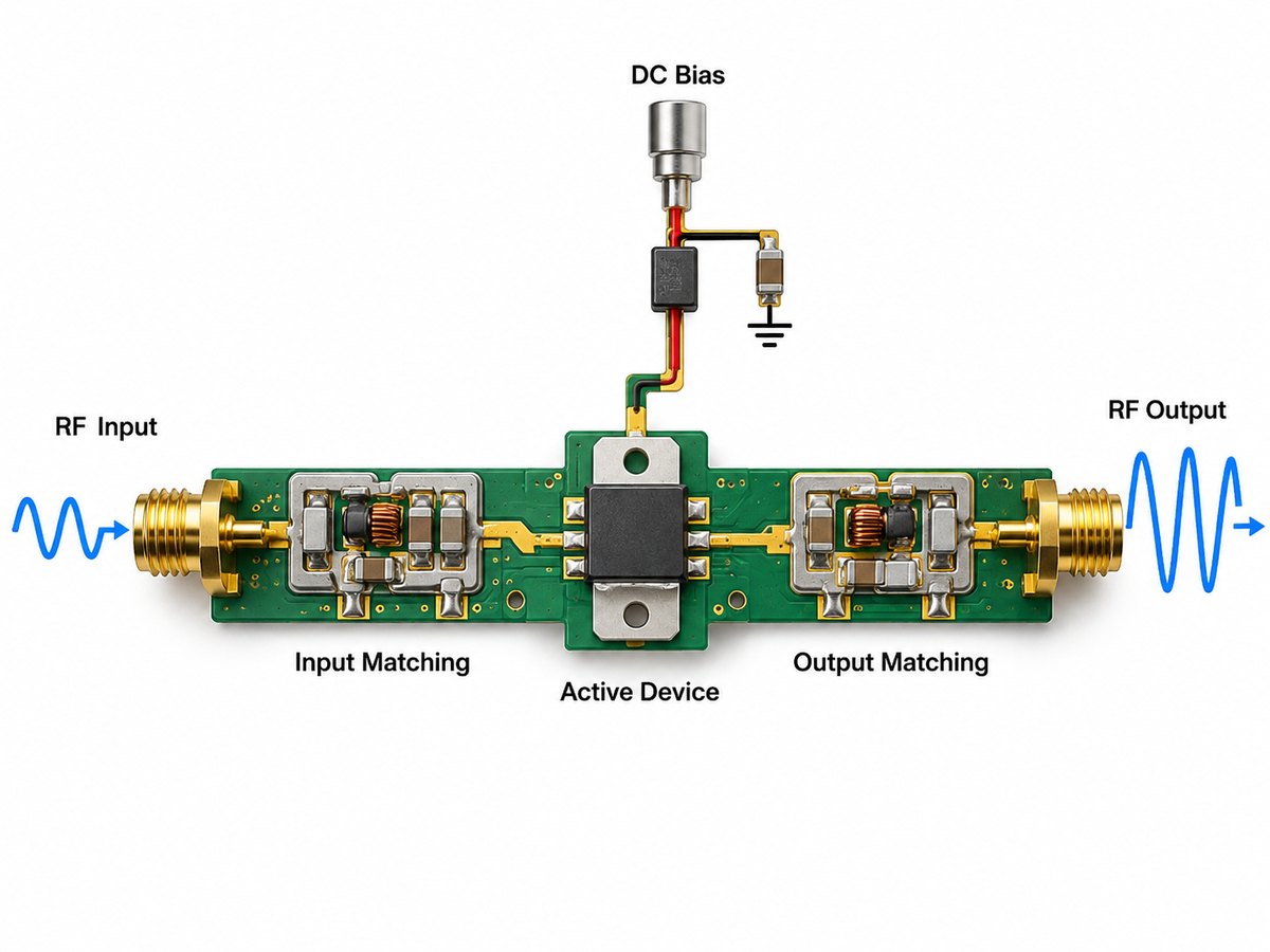
An RF amplifier uses energy from a DC power supply to increase the level of an incoming RF signal.

RF amplifier working principle showing input matching, active device, DC bias and output matching

A simplified RF signal path is:

RF input → input matching → active device → output matching → RF output

The active device may be a transistor, MMIC, or integrated RF amplifier IC. The surrounding network allows that device to operate at the required frequency and bias point.

A typical circuit includes:

  • Input matching network to interface the source with the amplifier
  • Active device to provide gain
  • Bias circuit to set the correct DC operating condition
  • Output matching network to transfer power to the next stage
  • Decoupling components to keep RF energy out of the power rail
  • DC blocking capacitors where RF and DC paths must be separated

At low input levels, the amplifier normally operates in its linear region. As input power rises, the output eventually stops increasing proportionally. This is the beginning of gain compression, which is why RF designers check parameters such as P1dB when defining the usable signal range.

What Are the Main Types and Classes of RF Amplifiers?

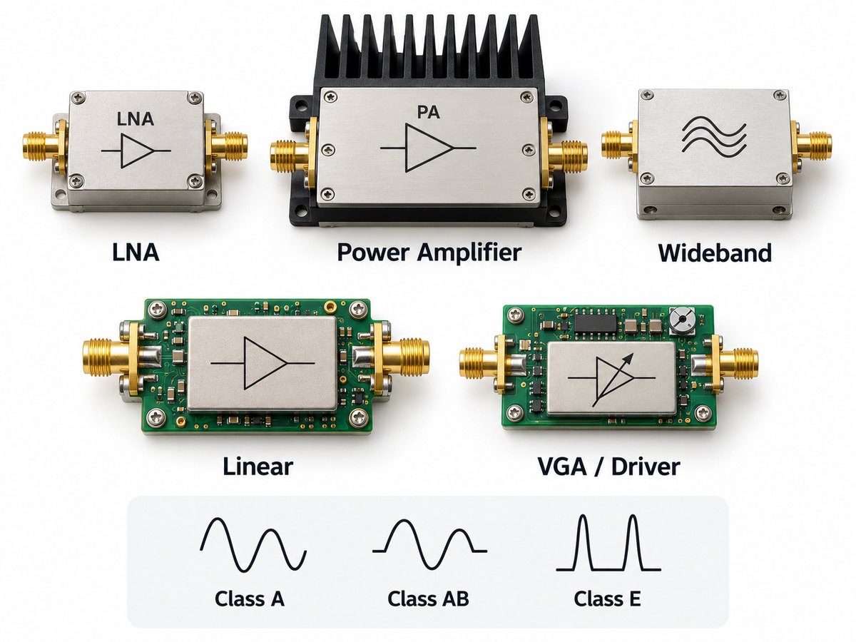
RF amplifiers are usually classified first by what they do in the RF signal chain.

Main RF amplifier types including LNA, power amplifier, wideband, linear and VGA driver amplifiers

Low-noise amplifier

A low-noise RF amplifier, or LNA, is used near the receiver input. Its main job is to amplify weak signals while adding as little noise as possible.

RF power amplifier

An RF power amplifier increases signal power before transmission. Output power, efficiency, linearity, and thermal performance are usually the main concerns.

Wideband RF amplifier

A wideband amplifier provides useful gain across a broad frequency range. It is common in test equipment, broadband communication, radar, and multi-band RF systems.

RF linear amplifier

A linear RF amplifier is designed to preserve the amplitude and phase characteristics of the input waveform. This matters for modulation schemes that are sensitive to distortion.

Variable gain amplifier

A VGA allows gain to be changed electronically. It is often used in automatic gain control and systems with a wide input signal range.

Gain block and driver amplifier

A gain block provides convenient fixed gain. A driver amplifier raises the signal level before another stage, often before the final PA.

RF power amplifiers may also be described as Class A, AB, B, C, D, or E. These classes describe how the active device operates.

In simple terms:

  • Class A favors linearity
  • Class AB balances linearity and efficiency
  • Class B and C increase efficiency but reduce linear operation
  • Class D and E use switching behavior for higher efficiency in suitable RF designs

Function and operating class are different classifications, so a power amplifier can still be described separately as Class AB, Class E, or another class.

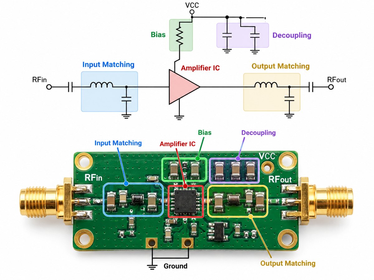
What Does an RF Amplifier Circuit and Schematic Include?

An RF amplifier circuit normally combines an active device with matching, bias, decoupling, and filtering networks.

RF amplifier circuit and schematic showing amplifier IC, bias, decoupling and input and output matching

The main parts shown in an RF amplifier schematic are typically:

  • Transistor, MMIC, or RF amplifier IC
  • Input matching components
  • Output matching components
  • Bias resistors, inductors, or RF chokes
  • DC blocking capacitors
  • Power-supply bypass capacitors
  • Ground connections
  • Optional filtering or stability components

The schematic shows the electrical connections, but the physical PCB implementation strongly affects the final RF behavior.

For example, a capacitor connected directly to ground on the schematic still has pad, trace, and via inductance on the real board. At microwave frequencies, even a short connection can change the response of the matching or decoupling network.

RF amplifier circuits may be implemented in three common forms:

  • Discrete circuit: transistor plus external bias and matching components
  • RF amplifier IC or MMIC: more RF functions integrated into one device
  • RF amplifier module: amplifier plus additional matching, shielding, connectors, filtering, or thermal structure

The best form depends on frequency, power, board area, development effort, and performance requirements.

Which RF Amplifier Specifications Matter Most?

The most important RF amplifier specifications are frequency range, gain, noise figure, linearity, output power, matching, and efficiency.

RF amplifier test setup and key specifications including gain, noise figure, P1dB, IP3, return loss and efficiency
Specification What It Indicates Typical Importance
Frequency range Supported RF band All RF amplifiers
Gain Signal amplification All signal chains
Gain flatness Gain variation across bandwidth Wideband systems
Noise figure Noise added by the amplifier Receiver LNAs
P1dB Beginning of meaningful gain compression Large-signal operation
IP3 Intermodulation linearity Multi-signal environments
Output power Available RF power Driver and power amplifiers
Return loss / VSWR Input and output matching RF interfaces
Efficiency DC-to-RF power conversion Power amplifiers
Supply voltage/current Electrical power requirement Power and thermal design

No single specification tells the whole story.

A high-gain amplifier may still be unsuitable if its output compresses too early. A low-noise device may not provide enough linearity in the presence of strong nearby signals. A power amplifier may meet its output-power target but create excessive heat if efficiency is poor.

For wideband designs, these specifications should be checked across the complete operating frequency range rather than only at the center frequency.

How Do Gain, Noise Figure, and Linearity Affect RF Amplifier Performance?

Gain, noise figure, and linearity determine how strongly an RF amplifier boosts the signal, how much noise it adds, and how well it handles larger or multiple signals.

Gain determines how much the signal level rises through the amplifier. Too little gain may leave the next stage with insufficient signal. Too much gain can reduce available headroom.

Noise figure measures how much the amplifier degrades the signal-to-noise ratio. It matters most in the early stages of a receiver, where added noise can directly affect sensitivity.

Linearity describes how well the amplifier avoids distortion as signal level rises. P1dB and IP3 are commonly used to judge this behavior.

These parameters often interact.

For example, increasing front-end gain can reduce the relative noise contribution of later receiver stages. However, the same higher gain may cause the receiver to reach compression sooner when a strong signal enters the system.

The priority depends on amplifier position:

  • LNA: noise figure, gain, linearity
  • Driver amplifier: gain, IP3, P1dB
  • Power amplifier: output power, efficiency, linearity, thermal performance

The correct target is therefore not simply maximum gain or minimum noise, but enough margin for the full signal environment.

How Do You Choose the Right RF Amplifier for an Application?

Choose an RF amplifier by matching its operating limits to the actual frequency, signal level, bandwidth, and system role.

Start with these requirements:

  • Operating frequency or frequency range
  • Required gain
  • Minimum and maximum input level
  • Required output power
  • Bandwidth
  • Noise figure limit
  • P1dB and IP3 targets
  • Modulation and linearity requirements
  • Supply voltage and current
  • Efficiency target
  • Operating temperature
  • Package or module size
  • Input and output impedance

For a receiver front end, noise figure and linearity are usually more important than maximum output power.

For a transmitter, output power, efficiency, linearity, compression, and thermal performance move higher on the list.

For a wideband RF amplifier, check that gain flatness, return loss, noise figure, and output performance stay acceptable across the full band.

It is also useful to check whether the manufacturer provides a validated evaluation-board layout. RF amplifier performance can change noticeably when the matching network or PCB geometry differs from the reference design.

What Causes RF Amplifier Instability and Oscillation?

RF amplifier instability is usually caused by unintended feedback, poor grounding, incorrect matching, or parasitic coupling.

Common causes include:

  • Coupling between RF input and output
  • Long or poorly controlled RF traces
  • Weak ground connections
  • Insufficient power-supply decoupling
  • Bias network problems
  • Incorrect matching components
  • Parasitic capacitance and inductance
  • Coupling through power or ground networks
  • Layout changes from the reference design
  • Poor isolation from digital or switching circuits

Oscillation may occur inside or outside the intended RF band. It can raise current consumption, increase noise, distort gain, or produce unexpected spectral components.

Several layout practices help reduce the risk:

  • Keep input and output networks physically separated
  • Place decoupling components close to the device pins
  • Use short ground paths
  • Add ground vias where needed
  • Keep switching power circuits away from sensitive RF sections
  • Preserve the intended matching-network geometry

For discrete RF amplifier design, stability should also be checked in simulation over a frequency range wider than the required operating band.

What PCB Design Factors Affect RF Amplifier Performance?

RF amplifier PCB performance depends heavily on controlled impedance, grounding, component placement, isolation, dielectric properties, and thermal design.

RF amplifier PCB design factors including controlled impedance, matching, via stitching, grounding, isolation and thermal path

Controlled impedance

RF traces are commonly designed as microstrip, stripline, or grounded coplanar waveguide. Their impedance depends on trace width, copper thickness, dielectric thickness, Dk, and nearby reference conductors.

RF trace routing

Critical RF paths should remain compact and free from unnecessary bends or discontinuities. The production routing should stay close to the geometry used during simulation or reference-board validation.

Grounding

A continuous ground reference helps maintain a predictable RF return path. Ground-plane gaps or long ground connections add unwanted inductance.

Matching-network placement

Matching capacitors and inductors should be positioned close to the RF device and in the intended order. At higher frequencies, moving these components can alter the matching response.

Via stitching

Ground stitching vias can help maintain plane continuity and reduce field spreading around RF structures.

Isolation

Keep RF inputs away from high-power RF outputs, clocks, DC/DC converters, and fast digital signals to reduce unwanted coupling.

PCB material

Higher-frequency or lower-loss designs may require RF laminates with more stable Dk and lower dissipation loss than standard FR-4. Material selection should match the loss budget, frequency, stackup, and cost target.

Thermal path

Power amplifiers may require:

  • Exposed thermal pads
  • Thermal vias
  • Heavy local copper
  • Heat spreaders
  • Metal chassis contact
  • Dedicated heatsinks

The fabricated PCB stackup should match the stackup used for impedance calculation and RF simulation. Changes to dielectric thickness, copper weight, or laminate grade can alter the final RF transmission-line geometry.

If your project is already moving from amplifier selection to board layout, our RF amplifier PCB guide explains the PCB-level checks that should be reviewed before fabrication and assembly.

Where Are RF Amplifiers Used?

RF amplifiers are used in receivers, transmitters, measurement equipment, medical systems, radar, wireless hardware, and microwave electronics.

Common applications include:

  • Cellular base stations
  • Wi-Fi and 2.4 GHz wireless devices
  • Bluetooth and IoT products
  • Satellite communication
  • Radar
  • GNSS receivers
  • Software-defined radio
  • RF test instruments
  • Microwave communication links
  • Radio transmitters
  • MRI systems
  • Industrial RF equipment
  • RF distribution systems
  • Aerospace and defense electronics

The amplifier type depends on the position in the system.

A receiver may use an LNA to raise a weak antenna signal. A transmitter may use a driver amplifier followed by a power amplifier. Test equipment may use wideband or variable gain amplifiers to support multiple frequency ranges and signal levels.

A 2.4 GHz RF amplifier, for example, can be used in either the receive or transmit chain. The required gain, noise figure, power, and linearity will differ depending on that role.

FAQ About RF Amplifiers

1. What does RF amplifier stand for?

RF amplifier stands for radio frequency amplifier. It amplifies RF signals used in wireless, radio, radar, satellite, and other high-frequency electronic systems.

2. What is the difference between an RF amplifier and an RF power amplifier?

An RF amplifier is the general category. An RF power amplifier is a specific type designed to deliver higher RF output power, usually near the transmitter output.

3. What is the difference between an LNA and a power amplifier?

An LNA amplifies weak received signals while adding very little noise. A power amplifier increases RF power for transmission or for driving another high-power stage.

4. What does gain mean in an RF amplifier?

Gain is the increase in signal level from the amplifier input to its output. RF power gain is usually expressed in decibels, or dB.

5. Why are RF amplifiers usually designed for 50 ohms?

Many RF cables, connectors, instruments, antennas, and components use 50 Ω interfaces, so 50 Ω has become a common system standard. Matching networks may still be required because the amplifier device itself may not have a native 50 Ω impedance.

6. Can an RF amplifier work at 2.4 GHz?

Yes. Many RF amplifiers are designed for the 2.4 GHz band. The device must support the required frequency while meeting the target gain, noise figure, output power, linearity, and matching requirements.

Ready to Move Your RF Amplifier Design Into PCB Production?

RF amplifier performance can change when the production PCB does not reproduce the intended stackup, impedance, grounding, matching geometry, component placement, or thermal path.

EBest Circuit supports RF and microwave PCB and PCBA projects using controlled impedance, Rogers materials, Rogers/FR-4 hybrid stackups, low-loss multilayer construction, HDI, fine-pitch assembly, impedance verification, and engineering DFM review. Send your Gerber files, stackup, BOM, target impedance, operating frequency, assembly requirements, and quantity to sales@bestpcbs.com for review and quotation.

You may also like

Half Duplex vs Full Duplex: Differences, Examples and Uses

September 10th, 2026

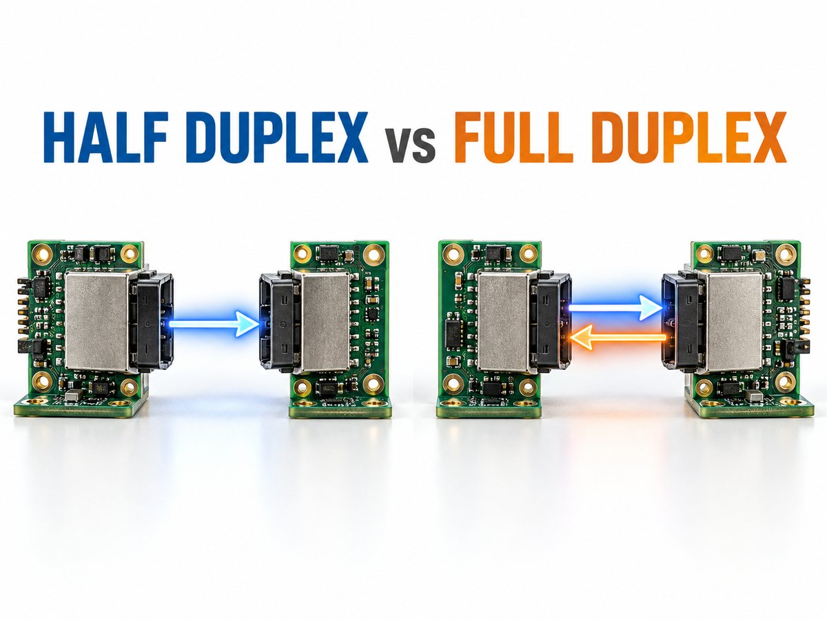
Half duplex vs full duplex explains how data moves between two connected devices. Half-duplex communication supports transmission in both directions, but only one device can transmit at a time. Full-duplex communication allows both devices to transmit and receive simultaneously. This difference affects wiring, throughput, latency, transceiver selection and software control.

Half duplex vs full duplex communication appears frequently in Ethernet networks, RS-485 buses, UART connections and SPI interfaces. However, an interface should not be classified by name alone. The physical wiring, transceiver, peripheral configuration and communication protocol all help determine whether the final system operates in half- or full-duplex mode.

Half duplex vs full duplex communication comparison

What Is Half Duplex Communication?

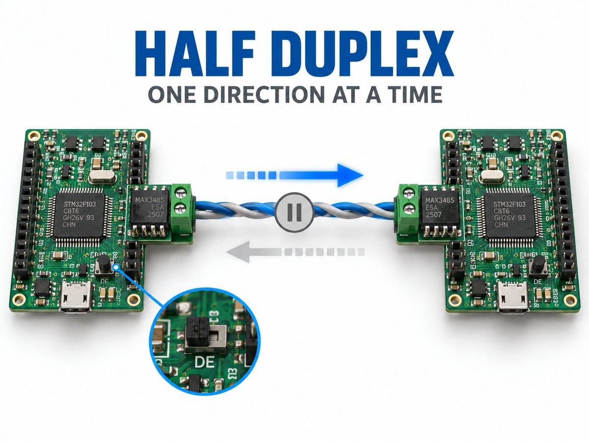
Half duplex is two-way communication in which the connected devices take turns transmitting. When one device sends, the other receives; the direction can reverse only after the active transmitter releases the channel.

Half duplex communication using one shared channel and alternating data direction

A walkie-talkie is the clearest example: both users can speak and listen, but not at the same time. Likewise, nodes on a 2-wire RS-485 network share one differential pair, and only one driver should control it at any moment.

Changing direction creates a short turnaround period. The controller must finish the last byte, disable its driver and release the channel. Poor timing can truncate data or activate two drivers together.

Half duplex is commonly used when:

  • Messages follow a request-and-response pattern.
  • Simultaneous data flow is unnecessary.
  • Several nodes share one physical bus.
  • Fewer wires and connector pins are preferred.
  • The system can tolerate a direction-change delay.

Examples include walkie-talkies, Ethernet hubs, 2-wire RS-485 and many Modbus RTU networks.

What Is Full Duplex Communication?

Full duplex is two-way communication that allows both devices to transmit and receive at the same time. Neither side needs to wait for the other to release the communication channel before sending data.

Full duplex communication with simultaneous transmit and receive paths

A telephone call is a familiar example. In electronics, UART commonly uses separate TX and RX lines, while 4-wire RS-485 uses one differential pair for each direction.

Some interfaces use signal separation or echo cancellation to send and receive over the same medium. The deciding factor is whether useful data can travel both ways simultaneously, not the wire count alone.

Full duplex is usually selected when:

  • Both devices generate data independently.
  • Low response latency is important.
  • Traffic is continuous in both directions.
  • Waiting to reverse the channel would limit performance.
  • The design can support the required signal paths and hardware.

Examples include switched Ethernet, telephone systems, separate-line UART and conventional four-wire SPI.

Half Duplex vs Full Duplex: What Are the Key Differences?

The main difference between half duplex and full duplex is whether simultaneous transmission is possible. Half duplex shares the channel between directions, while full duplex keeps both directions available at once.

Comparison Half Duplex Full Duplex
Data direction Two-way Two-way
Simultaneous send and receive No Yes
Channel access Devices take turns Both directions stay active
Turnaround delay Required Normally unnecessary
Direction control Often required Usually not required on point-to-point links
Bidirectional capacity Shared Available in both directions
Wiring Often fewer conductors May require separate signal paths
Typical use Shared buses and request-response traffic Continuous, low-latency communication

Half duplex suits shared buses and lower wire counts. Full duplex suits continuous two-way traffic but may require additional signal paths or processing resources.

Simplex vs Half Duplex vs Full Duplex: How Does Data Flow?

Simplex carries data in one fixed direction, half duplex carries data in both directions at different times, and full duplex carries data in both directions simultaneously.

Mode Data flow Can roles reverse? Simultaneous transmission? Example
Simplex One direction No No Broadcast receiver
Half duplex Two directions, one at a time Yes No Walkie-talkie
Full duplex Two directions at once Yes Yes Telephone

A sensor that only reports measurements can use simplex communication if it never receives commands. A shared industrial bus often uses half duplex because every node can transmit when given access. A real-time point-to-point link may use full duplex so control data and feedback can move concurrently.

The required data flow decides the mode; the more capable-sounding option is not automatically the better fit.

Half Duplex vs Full Duplex Ethernet: How Do Switches and Auto-Negotiation Work?

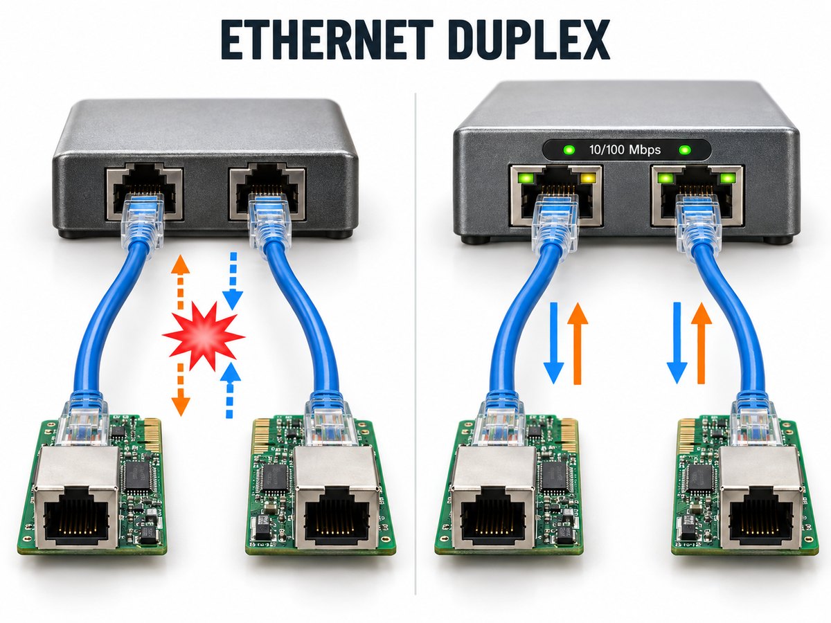
Half-duplex Ethernet is associated mainly with shared media and hubs, while modern point-to-point switch connections normally operate in full duplex.

Half duplex and full duplex Ethernet with 10 and 100 Mbps connections

With an Ethernet hub, all devices share one collision domain. Simultaneous transmissions collide and must be resent, so half-duplex Ethernet uses CSMA/CD to control access.

A switch gives each device a dedicated link, allowing simultaneous transmission and reception without normal Ethernet collisions. That is why switched networks normally use full duplex.

Auto-negotiation lets the switch and network interface select a shared speed and duplex mode. If the settings differ, the link may remain active but perform poorly.

Common signs of a duplex mismatch include:

  • Low or inconsistent throughput
  • Late collisions on the half-duplex side
  • Frame errors and retransmissions
  • Intermittent application response
  • Better performance in one direction than the other

For current Ethernet equipment, leaving both ends on auto-negotiation is usually appropriate. When legacy hardware requires manual settings, configure the same speed and duplex mode at both ends.

10/100 Mbps Half Duplex vs Full Duplex: Does Full Duplex Double the Speed?

Full duplex doubles the theoretical bidirectional capacity of a 10 or 100 Mbps link, but it does not double its single-direction speed. A 100 Mbps full-duplex link can send at 100 Mbps and receive at 100 Mbps simultaneously; it cannot send one file at 200 Mbps.

The same rule applies to 10 Mbps Ethernet:

  • 10 Mbps half duplex shares 10 Mbps between both directions.
  • 10 Mbps full duplex provides 10 Mbps in each direction at the same time.
  • 100 Mbps half duplex shares 100 Mbps between sending and receiving.
  • 100 Mbps full duplex provides 100 Mbps in each direction simultaneously.

Full duplex matters most when traffic moves both ways. For mainly one-way transfers, storage speed, protocol overhead and network congestion may have greater impact.

RS-485 Half Duplex vs Full Duplex: What Changes Between 2-Wire and 4-Wire?

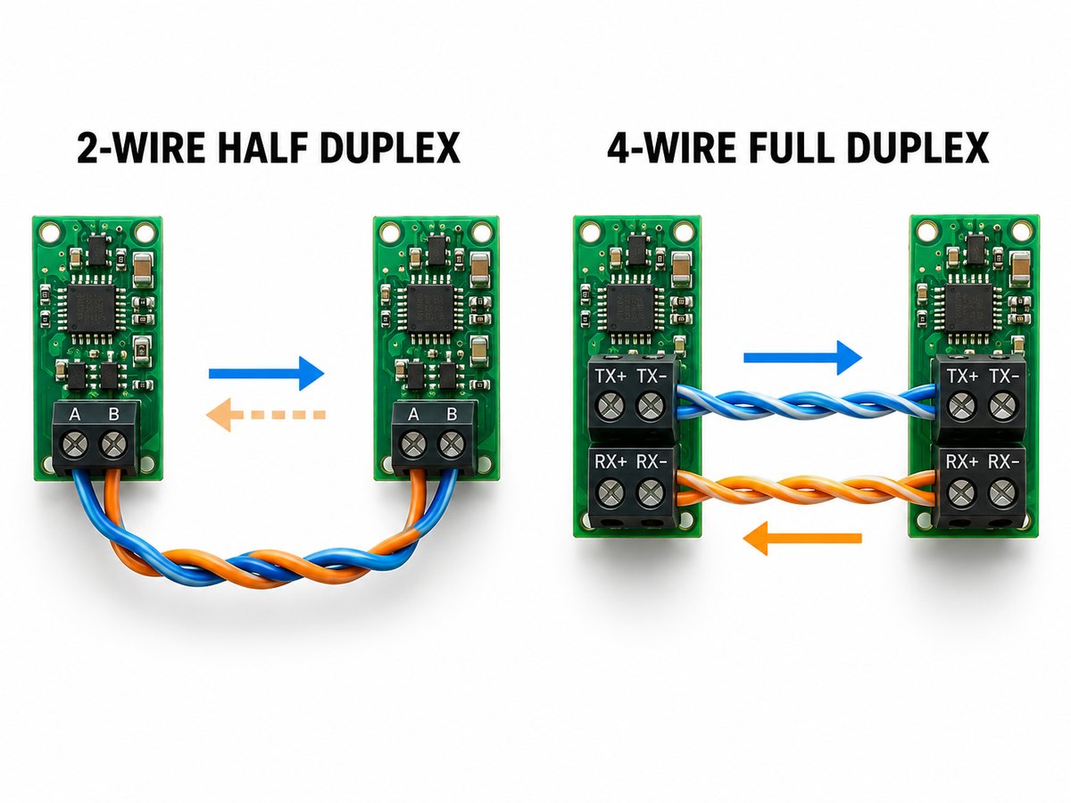
For a half duplex vs full duplex RS485 comparison, the main change is whether one pair is shared or separate pairs carry each direction. RS-485 half duplex normally uses one differential pair, while RS-485 full duplex uses two pairs—one for each direction. This changes the transceiver connection, cable, connector and direction-control requirements.

Two-wire half-duplex RS-485 compared with four-wire full-duplex RS-485

2-wire half-duplex RS-485

All drivers and receivers share one pair. The active node enables its driver, sends the message and releases the bus, usually through the transceiver’s DE and /RE controls.

The driver must stay enabled until the final bit leaves the UART and transceiver. Releasing it early cuts off the message; holding it too long delays the reply.

4-wire full-duplex RS-485

One pair carries master transmissions, and the other carries replies. The master can use both simultaneously, although slave drivers sharing the return pair still need controlled access.

Design factor 2-Wire RS-485 4-Wire RS-485
Duplex mode Half duplex Full duplex
Differential pairs One Two
Master send and receive Alternating Simultaneous
Cable and connector size Lower Higher
Direction control Required Depends on node role
Common use Multidrop request-response bus Continuous master communication

Modbus RTU commonly runs over 2-wire half-duplex RS-485. Its request-response sequence already assigns transmission turns, so adding another pair may not shorten the transaction. Modbus defines messaging; RS-485 defines the electrical connection.

SPI Half Duplex vs Full Duplex: How Do Data Lines and Transfers Differ?

Conventional SPI supports full-duplex transfer through separate MOSI and MISO lines, while half-duplex SPI shares one bidirectional data line.

A standard SPI connection usually includes:

  • SCLK for the clock
  • MOSI for controller-to-peripheral data
  • MISO for peripheral-to-controller data
  • CS or SS for peripheral selection

With separate MOSI and MISO paths, the controller transmits and samples one bit per clock cycle. Both streams are not always meaningful: a memory may receive a command first and return data later while the controller sends dummy bytes to generate the clock.

Three-wire SPI combines input and output on one SDIO line. It saves a pin and trace but requires direction switching, turnaround time and compatible devices.

Classify an SPI link from its wiring and transaction format, not from the protocol name alone.

UART Half Duplex vs Full Duplex: How Do TX and RX Connections Differ?

UART is full duplex when separate TX and RX lines operate simultaneously, but it becomes half duplex when transmission and reception share one external path.

In a full-duplex UART link, each device’s TX connects to the other’s RX, with a shared ground reference. Both peripherals can communicate without changing pin direction.

Half-duplex UART can be created in two common ways:

  • A single-wire UART mode shares one bidirectional signal.
  • A UART connects through a 2-wire RS-485 transceiver that combines the external transmit and receive paths.

With RS-485, the MCU may retain separate TX and RX signals while the external bus remains half duplex. Firmware or the transceiver must then control direction.

The UART block defines asynchronous character framing. The schematic and line transceiver determine the external voltage levels, wiring and duplex mode.

How Does Half Duplex vs Full Duplex Affect PCB Interface Design?

Duplex mode affects PCB routing, component count, connectors, protection and firmware control. It should be confirmed before the schematic and layout are released.

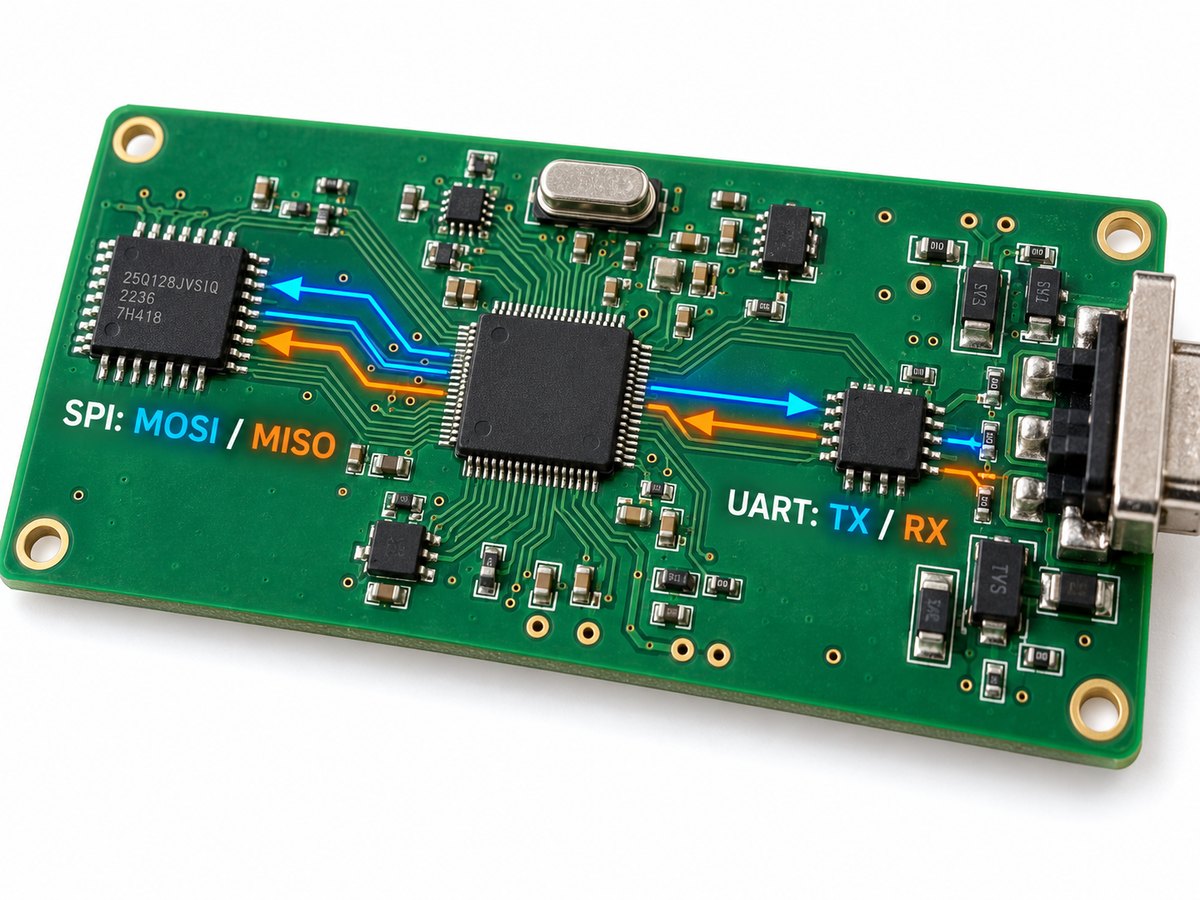
SPI MOSI and MISO routing with UART TX and RX connections on a PCB

Review these design areas:

  • Signal count: A shared half-duplex path can save MCU pins, traces and connector contacts. Full-duplex differential communication may require twice as many signal pairs.
  • Transceiver pinout: Half-duplex RS-485 parts often combine driver outputs and receiver inputs. Full-duplex parts expose separate bus connections.
  • Direction control: Shared buses need reliable DE and /RE timing, including the UART shift-register delay after the final byte is written.
  • Routing: Differential pairs need consistent spacing, short stubs and a continuous reference path. Two full-duplex pairs also require more board and connector space.
  • Termination and biasing: Component values and locations should match the cable impedance and topology. RS-485 cabling commonly uses approximately 120 Ω differential termination.
  • Protection: External ports may need ESD, surge or EFT protection. Industrial interfaces may also require galvanic isolation.
  • Production testing: Tests should verify polarity, termination, direction switching, idle-bus state and communication at the specified data rates.

Select half duplex when lower wire count and shared-bus access outweigh turnaround delay. Select full duplex when simultaneous traffic and predictable response time justify the additional signal paths.

FAQs About Half Duplex vs Full Duplex

1. Is full duplex always faster than half duplex?

Not necessarily for every task. Full duplex provides greater bidirectional capacity because sending and receiving can occur simultaneously, but a one-way transfer remains limited by the link’s rated speed and the rest of the system.

2. Can an Ethernet switch operate in half duplex?

Some 10/100 Mbps switch ports support both modes for compatibility with older equipment. Modern switched networks normally use full duplex, while current Gigabit Ethernet connections are generally operated in full duplex.

3. What causes a duplex mismatch?

A duplex mismatch occurs when one end of a link uses half duplex and the other uses full duplex. It is commonly caused by inconsistent manual settings or failed auto-negotiation and can produce low throughput, collisions and frame errors.

4. Is Modbus RTU half duplex or full duplex?

Modbus RTU does not inherently require only one duplex mode, but it is commonly used over 2-wire half-duplex RS-485. Its request-response communication pattern fits naturally with devices taking turns on a shared bus.

5. Is RS-422 half duplex or full duplex?

RS-422 is commonly used with separate transmit and receive differential pairs, creating a full-duplex connection. The precise operating mode still depends on how the channels and transceivers are implemented.

6. Can one interface support both half duplex and full duplex?

Yes, if the controller, transceiver and connector provide the required modes and signal paths. Some configurable UART peripherals and RS-485 transceivers support both, but the PCB must include the necessary routing and control connections.

If you are developing equipment or embedded systems with Ethernet, RS-485, SPI, UART or another wired interface, confirm the duplex mode before finalizing the transceiver, connector and PCB interface design. EBest Circuit can review the Gerber files, BOM, schematic, controlled-impedance requirements and assembly data together before production.

Send your project files and interface requirements to sales@bestpcbs.com for PCB manufacturing, PCBA and engineering review.

You may also like

What Is Co-Packaged Optics (CPO)? Technology, Applications, Challenges, and PCB Design

September 10th, 2026

Co-Packaged Optics (CPO) is an optical interconnect architecture that places optical engines close to high-bandwidth chips such as switch ASICs, processors, and accelerators. By shortening the electrical path between the chip and the optical interface, CPO can reduce high-speed signal loss, lower I/O power, and support much higher bandwidth density than conventional front-panel pluggable optics.

CPO is moving from an emerging concept into real high-capacity networking hardware, driven particularly by AI data centers and hyperscale computing. For hardware engineers, this shift also changes how advanced packaging, thermal management, fiber routing, power delivery, PCB stackups, and system integration are approached.

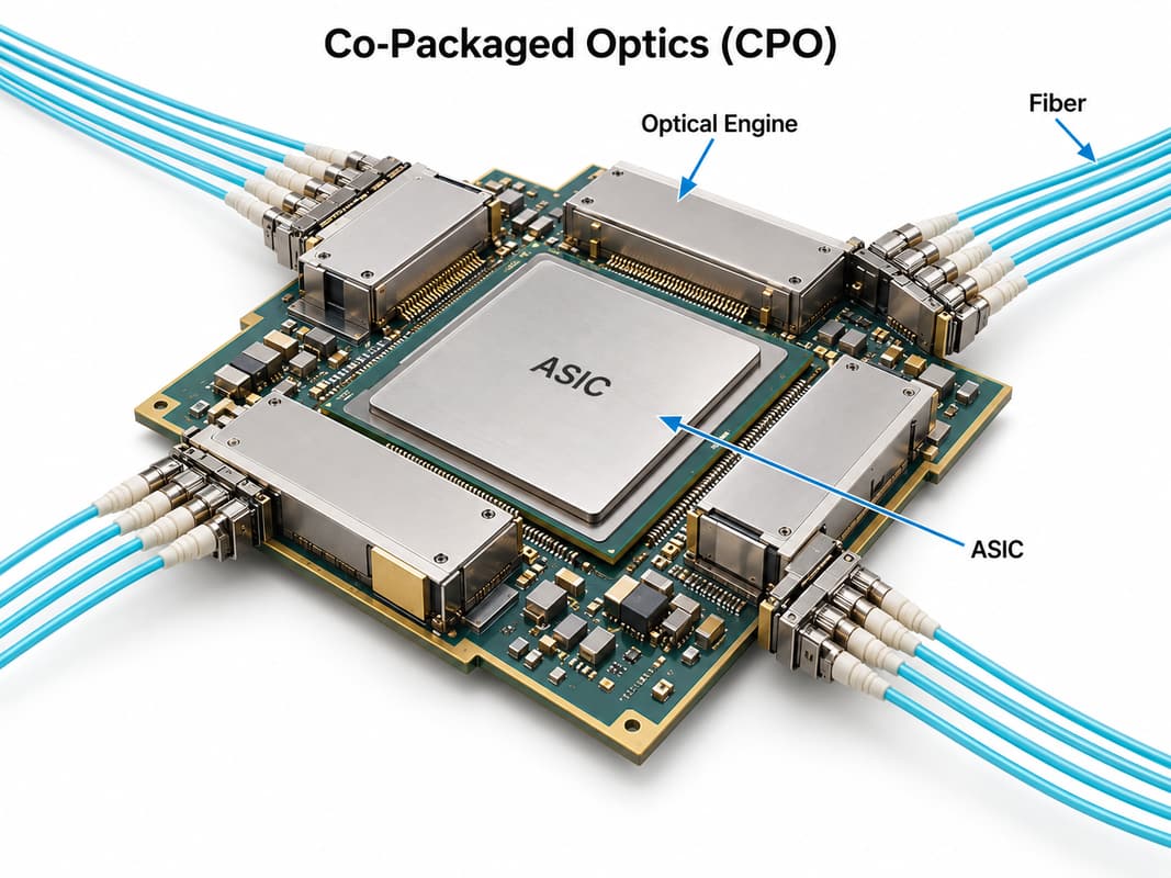
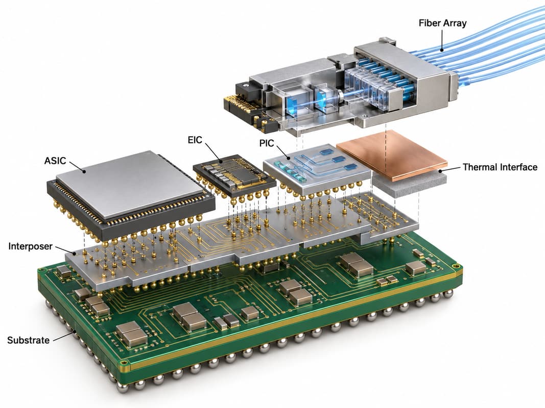
Co-Packaged Optics CPO architecture with ASIC, optical engines and fiber

What Is Co-Packaged Optics (CPO)?

Co-Packaged Optics integrates optical engines within or immediately beside the package of a high-performance electronic chip, allowing high-speed electrical signals to travel only a short distance before being converted to light.

In a conventional pluggable-optics architecture, signals travel from the ASIC across the PCB to optical transceivers installed at the front panel. CPO moves this electrical-to-optical conversion much closer to the silicon.

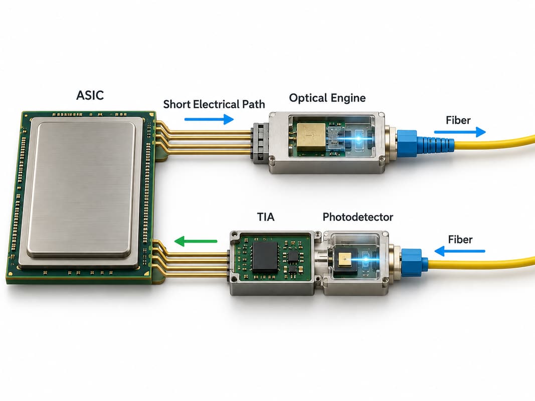
ASIC or processor → short electrical connection → optical engine → fiber

The package can contain separate electronic and photonic dies rather than integrating every function onto one chip. CPO is therefore an optical and electronic integration architecture, not a single type of optical component.

How Does Co-Packaged Optics Work?

Co-Packaged Optics works by converting high-speed electrical data into optical signals close to the ASIC or processor and carrying the longer-distance portion of the link over fiber.

Co-Packaged Optics transmit and receive signal flow from ASIC to optical engine and fiber

A typical transmit path is:

  • The ASIC generates high-speed electrical data.
  • A short electrical connection carries it to the optical engine.
  • Driver electronics prepare the signal.
  • A photonic integrated circuit modulates light with the data.
  • Fiber carries the optical signal to another device.

The receive path reverses the process:

  • Fiber delivers the incoming optical signal.
  • A photodetector converts light into an electrical signal.
  • A TIA and related electronics process the signal.
  • The data reaches the ASIC over a short electrical connection.

Many CPO architectures use an external laser source (ELS). Light is generated away from the ASIC and delivered to the optical engine through fiber. OIF has standardized external-laser approaches for co-packaged optical systems through its ELSFP work, including field-replaceable laser modules.

What Technologies Make Co-Packaged Optics Possible?

CPO relies on silicon photonics, photonic integrated circuits, high-speed electronics, precision optical coupling, and heterogeneous integration working together.

Silicon photonics

Silicon photonics enables optical functions such as waveguides, modulators, couplers, and photodetectors to be fabricated in compact semiconductor-based devices.

Photonic integrated circuits

The PIC handles functions such as optical modulation, detection, routing, and coupling. Multiple optical channels can be integrated into one photonic engine to increase aggregate bandwidth.

High-speed electronic ICs

Drivers, TIAs, clocking circuits, and other interface electronics connect the optical section to the main ASIC.

External laser technology

Many architectures separate the laser from the optical engine to improve thermal conditions and serviceability.

Precision optical coupling

Fiber must be accurately aligned with the photonic interface. Small positional errors can increase coupling loss, so optical assembly requires much tighter mechanical control than ordinary board-level connectors.

These technologies provide the functional building blocks. Bringing them into one compact hardware platform is primarily an advanced-packaging task.

Co-Packaged Optics vs Pluggable Optics: What Is the Difference?

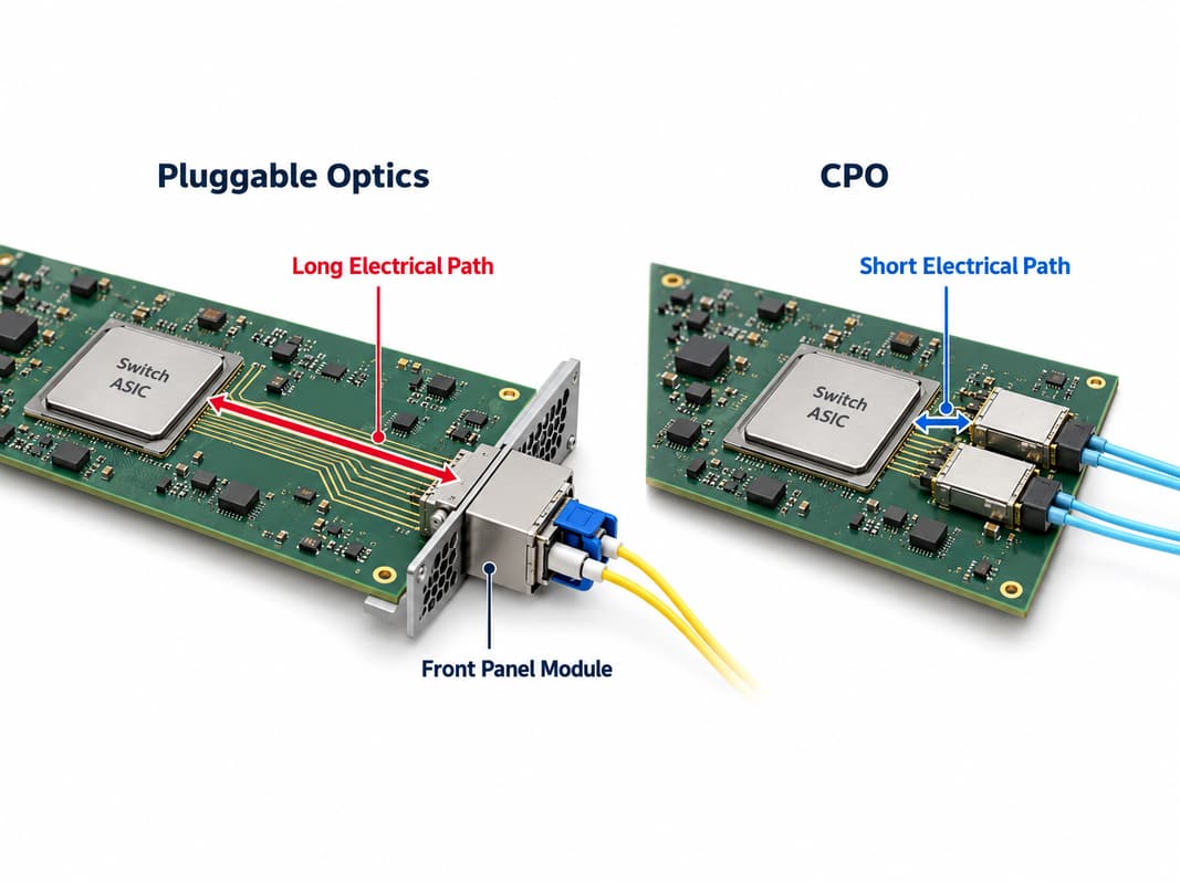
The main difference between Co-Packaged Optics and pluggable optics is the location of the optical engine: CPO places it close to the ASIC, while pluggable optics keeps the optical module at the system faceplate.

Comparison of Co-Packaged Optics and pluggable optics showing short versus long electrical paths
Item Pluggable Optics Co-Packaged Optics
Optical engine location Front panel Close to ASIC
High-speed electrical path Relatively long Very short
PCB channel demand Higher Reduced near optical interface
Electrical loss Higher at very high rates Lower
Bandwidth density Limited by faceplate space Potentially much higher
Module replacement Simple More complex
Packaging Mature and modular Highly integrated
Thermal design Module and ASIC more separated Optics and ASIC interact closely
Deployment maturity Widely established Entering broader production

Pluggable optics remains attractive because individual modules can be replaced or upgraded without disturbing the main switch package.

CPO trades some of that modularity for a shorter electrical path. The trade becomes more attractive as SerDes speed, channel loss, power consumption, and faceplate density become harder to scale.

Co-Packaged Optics vs NPO vs LPO: How Do They Compare?

CPO, NPO, and LPO mainly differ in how close the optical engine sits to the ASIC and how much electrical processing remains between the ASIC and optics.

Architecture Optical Location Electrical Reach Serviceability Integration
Traditional pluggable Front panel Longest High Low
LPO Front panel Long High Low
NPO Near ASIC Short Moderate Medium
CPO At or within ASIC package environment Shortest More difficult Highest

Linear Pluggable Optics (LPO) retains a front-panel optical module while simplifying the signal-processing chain to reduce DSP-related power.

Near-Packaged Optics (NPO) places the optical engine near the ASIC without integrating it as tightly into the package.

Co-Packaged Optics (CPO) moves optics closest to the ASIC and has the highest degree of integration.

As the optical engine moves closer to the ASIC, electrical reach generally falls, but package complexity and service requirements increase.

What Are the Main Benefits of Co-Packaged Optics?

The main CPO benefits are lower electrical channel loss, lower I/O power potential, greater bandwidth density, and better scalability at very high data rates.

They result mainly from shortening the ASIC-to-optics electrical path:

  • Lower electrical loss: shorter high-speed connections introduce less attenuation.
  • Lower I/O power potential: short channels can reduce the need for aggressive equalization, retimers, or additional signal conditioning.
  • Higher bandwidth density: optical bandwidth is less dependent on the number of pluggable modules that fit on the front panel.
  • Better bandwidth scaling: increasing ASIC bandwidth does not require every optical lane to traverse a long PCB channel.
  • Less demanding ASIC-to-optics board routing: much of this interface moves toward the package.

These advantages become more valuable as per-lane data rate and total system bandwidth rise.

What Are the Main Challenges of Co-Packaged Optics?

The main CPO challenges are thermal management, optical alignment, package yield, testing, fiber attachment, laser delivery, serviceability, and standardization.

  • Thermal management: high-power ASICs create a difficult environment for nearby optical devices.
  • Optical alignment: fiber-to-photonic interfaces require precise positioning to maintain coupling efficiency.
  • Package yield: one defective electronic or optical component can affect the value of a complex multi-die package.
  • Testability: both electrical and optical functions need to be screened before and after integration.
  • Fiber attachment: fiber arrays require repeatable alignment and adequate mechanical reliability.
  • External laser delivery: optical power must reach the photonic engines with controlled loss.
  • Serviceability: integrated optical engines are more difficult to replace than front-panel transceivers.
  • Standardization: electrical, optical, laser, package, and management interfaces are still developing.

Standardization is already progressing. OIF has published a 3.2 Tb/s co-packaged module implementation agreement as well as external-laser implementation agreements for CPO systems.

Why Is Co-Packaged Optics Important for AI Data Centers?

Co-Packaged Optics is important for AI data centers because large accelerator clusters require rapidly increasing network bandwidth while power and electrical-channel loss become harder to control.

As AI clusters scale, several requirements rise together:

  • GPU/XPU-to-GPU/XPU traffic
  • switch capacity
  • SerDes data rate
  • bandwidth density
  • network power consumption

CPO reduces the board-level electrical distance between the switching silicon and optics before moving the traffic onto fiber.

Commercial hardware now shows the scale involved. NVIDIA’s Spectrum-X Ethernet Photonics uses 200 Gb/s SerDes, and its SN6800 platform reaches 409.6 Tb/s total bandwidth. NVIDIA stated in May 2026 that Spectrum-X Ethernet Photonics CPO switches were in production as part of the Vera Rubin platform.

This makes CPO especially relevant to AI scale-up fabrics, scale-out networks, high-radix Ethernet, and other accelerator-heavy infrastructure.
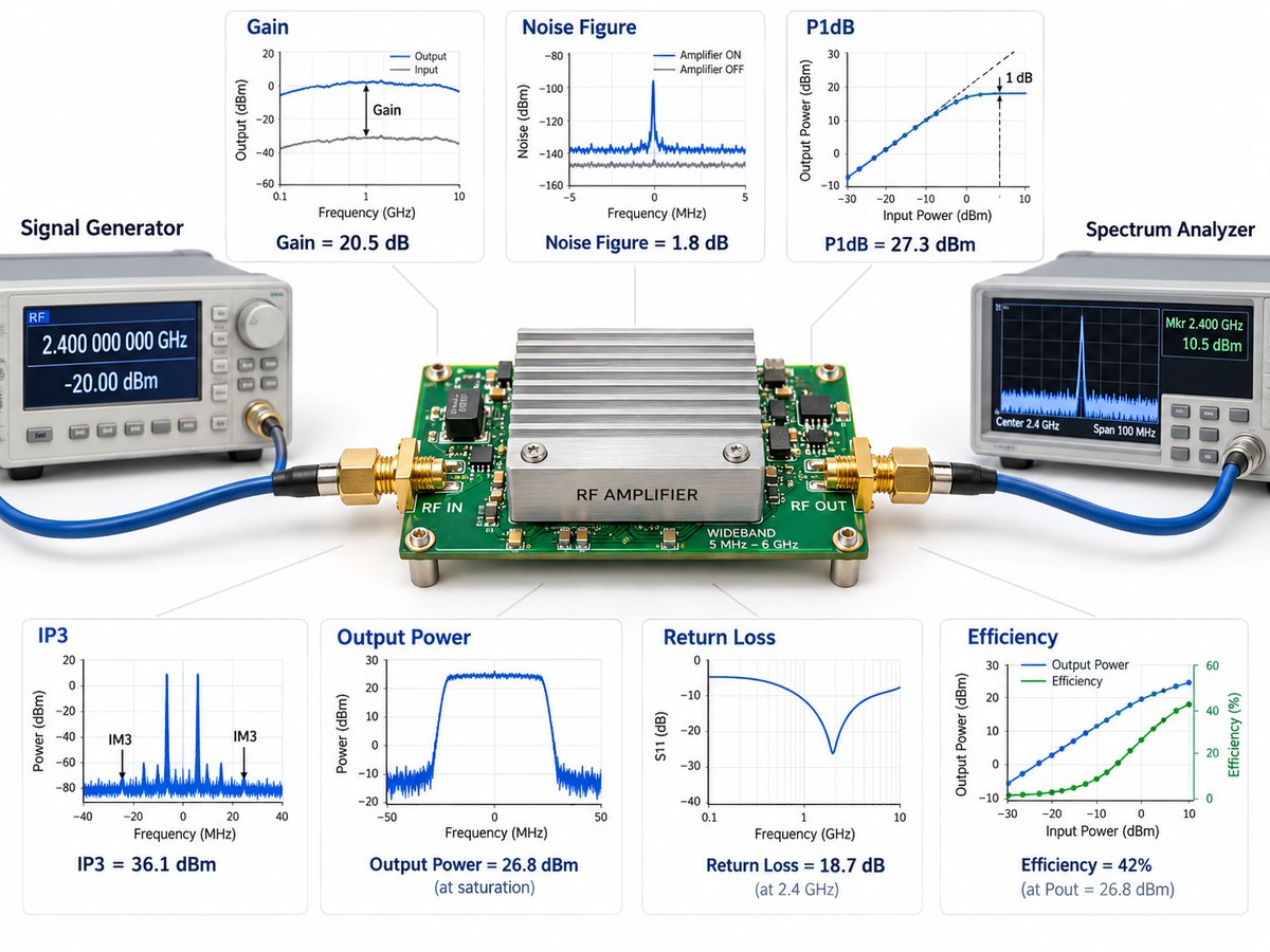
Where Is Co-Packaged Optics Used Today?

CPO is already entering production in AI and hyperscale networking, while applications such as direct processor optical I/O and broader disaggregated computing remain at earlier stages of adoption.

Co-Packaged Optics applications in AI data centers, hyperscale cloud and HPC optical fabrics

Current co-packaged optics applications include:

  • AI data center networks: CPO connects very high-capacity switching silicon to optical fabrics used between accelerator systems.
  • Hyperscale cloud networks: cloud operators face similar bandwidth-density and electrical-reach constraints as switch capacity increases.
  • High-performance computing: large HPC systems require high-bandwidth communication between compute nodes.
  • High-capacity Ethernet switching: switches are one of the clearest early commercial applications of CPO.
  • Large routing platforms: high-throughput networking equipment can benefit when front-panel density and long electrical channels limit further scaling.

Commercialization is no longer hypothetical. Broadcom announced its 102.4 Tb/s Tomahawk 6–Davisson CPO Ethernet switch in 2025 as its third-generation CPO platform, while NVIDIA reported production of Spectrum-X Ethernet Photonics systems in 2026.

Emerging applications include:

  • processor-to-processor optical I/O
  • GPU and XPU optical interfaces
  • chiplet-to-chiplet optical links
  • disaggregated compute and memory systems
  • future optical connections between separated compute resources

These emerging uses extend the same principle beyond network switching: convert data to light closer to the device when conventional electrical interconnect becomes inefficient in bandwidth, reach, or power.

How Does Advanced Packaging Support Co-Packaged Optics?

Advanced packaging supports CPO by placing electronic and photonic dies close enough to communicate over short, dense electrical connections while maintaining optical alignment and thermal control.

Exploded Co-Packaged Optics package showing ASIC, PIC, EIC, interposer, substrate, thermal interface and fiber array

A CPO assembly may combine:

  • switch or compute ASICs
  • PICs
  • electronic driver and receiver ICs
  • optical engines
  • organic package substrates
  • silicon or organic interposers
  • redistribution structures
  • micro-bumps or other fine-pitch connections
  • fiber coupling interfaces
  • thermal interfaces

The packaging architecture must solve three problems at once:

  • keep high-speed electrical interconnects short;
  • maintain accurate optical coupling;
  • provide an effective thermal path away from high-power silicon.

Depending on the platform, this may involve 2.5D integration, interposers, chiplets, fine-pitch redistribution, micro-bumps, or hybrid bonding.

How Does Co-Packaged Optics Change PCB and System Design?

CPO changes PCB design by moving some of the fastest ASIC-to-optics routing into the package while increasing the importance of board-level power delivery, dense breakout routing, thermal management, and mechanical integration.

The PCB still carries several critical responsibilities:

  • Power delivery: high-power ASICs and supporting electronics require low-impedance power distribution.
  • Remaining high-speed links: PCIe, memory, clocks, control, management, and other interfaces still need controlled signal integrity.
  • BGA escape routing: large advanced packages can require dense multilayer breakout.
  • Fiber-related mechanical layout: fiber exits, bend radius, connectors, cold plates, and heat sinks affect component placement.
  • Thermal integration: package position, PCB copper, airflow, and cooling hardware influence the complete thermal path.
CPO does not eliminate the PCB. It changes which PCB functions become most demanding.

Long ASIC-to-optics board traces can be reduced, while power, remaining high-speed connections, cooling, mechanical clearances, and package breakout remain board-level design concerns.

What PCB Requirements Matter in Co-Packaged Optics Systems?

CPO systems typically need PCBs with controlled impedance, suitable low-loss materials, dense multilayer routing, robust power distribution, accurate dimensions, and support for large advanced packages.

PCB requirements for Co-Packaged Optics including controlled impedance, HDI, BGA breakout, power layers, thermal vias and Rogers FR-4 hybrid stackup

Typical requirements include:

  • Low-loss laminate: for high-speed electrical links that remain on the board.
  • Controlled impedance: for SerDes, PCIe, clocks, and other high-speed channels.
  • HDI structures: microvias and sequential lamination may be needed for dense package breakout.
  • High layer count: signal, power, and ground routing can require complex stackups.
  • Power integrity: high-current ASICs need suitable planes, copper distribution, and via capacity.
  • Fine-pitch BGA routing: large advanced packages can require tight trace and via geometry.
  • Dimensional control: important around package, cooling, fiber, and connector interfaces.
  • Thermal structures: thermal vias, copper planes, copper inlays, or other heat-spreading features may be required.
  • Backdrilling: through-hole via stubs may need removal on sensitive high-speed channels.
  • Surface finish: the finish should match the assembly and reliability requirements.

The PCB specification should come from the actual channel, package, power, and mechanical requirements rather than from a generic “CPO PCB” stackup.

What Should You Consider When Manufacturing PCBs for CPO Hardware?

When manufacturing PCBs for CPO hardware, the main concerns are material selection, impedance control, stackup repeatability, HDI capability, power delivery, dimensional accuracy, thermal requirements, and prototype-to-production consistency.

A useful RFQ package should include:

  • PCB stackup
  • laminate grade or loss target
  • dielectric thickness
  • finished board thickness
  • copper weight
  • controlled-impedance values and tolerance
  • minimum trace and spacing
  • via and microvia structure
  • backdrill requirements
  • BGA pitch
  • dimensional tolerances
  • thermal requirements
  • surface finish
  • assembly drawings
  • prototype and production quantity

For high-speed channels, include the operating data rate and insertion-loss target when available.

At EBest Circuit, we bring more than 20 years of PCB and PCBA manufacturing experience to CPO-related hardware, with production capabilities in both China and Vietnam. We support low-loss multilayer PCBs, HDI, controlled impedance, fine-pitch BGA designs, advanced thermal structures, and complex stackups for high-speed systems where signal integrity, power delivery, and manufacturing consistency all matter.

Our advantage is not limited to board fabrication. For CPO and AI-related high-speed hardware, we have experience with Rogers materials such as RO4350B, RO4003C, RO3003, RO3010, and RT/duroid 5880, as well as Rogers/FR-4 hybrid multilayer constructions. We can combine material selection, controlled-impedance stackups, HDI routing, fine-pitch BGA breakout, thermal design, and PCBA in one manufacturing flow, supporting projects from prototype builds through volume production.

FAQs About Co-Packaged Optics

1. Is co-packaged optics the same as silicon photonics?

No. Silicon photonics is a technology used to create integrated optical components, while CPO is a system and packaging architecture that places optical engines close to high-performance electronic chips. Silicon photonics is one of the technologies that can enable CPO.

2. Will co-packaged optics replace pluggable optics?

Not completely. Pluggable optics offers strong serviceability, an established ecosystem, and simple replacement. CPO is more attractive where bandwidth density, electrical reach, and power become limiting factors. Both architectures are likely to coexist across different applications.

3. What is the difference between CPO and optical I/O?

CPO is a specific integration approach, while optical I/O is a broader concept. CPO commonly refers to optics integrated around switch or compute packages to replace longer electrical links. Optical I/O can also include direct optical interfaces on processors, accelerators, chiplets, and other semiconductor devices.

4. Why does CPO often use external lasers?

CPO often uses external lasers to separate the laser source from the hot ASIC environment. This can improve thermal conditions and simplify laser replacement. The optical engine receives laser light through fiber and uses that light for modulation.

5. Is co-packaged optics only used in AI data centers?

No. AI infrastructure is currently a major driver, but CPO can also support hyperscale cloud networks, HPC systems, high-capacity routers, telecom equipment, disaggregated computing, and emerging processor optical I/O.

6. What are the biggest barriers to CPO adoption?

The biggest barriers are manufacturing and integration complexity. Key issues include thermal management, packaging yield, optical alignment, fiber attach, manufacturing cost, test complexity, serviceability, laser architecture, and standardization.

7. Does CPO still require high-speed PCBs?

Yes. CPO shortens some of the highest-speed electrical paths, but the system still contains board-level high-speed links, power distribution, control interfaces, BGA routing, connectors, and other circuitry. PCB design remains an important part of the platform.

8. Which companies are developing co-packaged optics?

Leading co-packaged optics companies include Broadcom, NVIDIA, Marvell, Intel, Cisco, and Ayar Labs. The broader ecosystem also includes foundries, packaging companies, laser suppliers, fiber manufacturers, and optical-component suppliers working on different parts of the CPO platform.

If you are developing high-speed networking, AI hardware, optical I/O, or other CPO-related electronics, send your Gerber files, stackup, BOM, impedance requirements, and assembly drawings to sales@bestpcbs.com. We can review your PCB manufacturability, material selection, HDI structures, controlled impedance, thermal requirements, and PCBA needs before production.
Selected references

You may also like

What Are Embedded Systems? Components, Examples and PCB Design

September 8th, 2026

What are embedded systems? They are purpose-built computers integrated into products or machines to monitor inputs, make decisions, and control specific functions. An embedded system combines electronic hardware with firmware or software, and it is normally designed around limits such as response time, power, size, operating environment, and cost.

A simple thermostat and a multi-board industrial controller can both be embedded systems. Their complexity differs, but the design question is the same: can the hardware and software perform the required function predictably inside the finished product?

Embedded control PCB connecting a sensor input to a motor output

What Is an Embedded System?

An embedded system is a computer built into a larger product to perform a defined function or a limited group of related functions. It may be nearly invisible to the user, yet it can control sensing, communication, motion, power conversion, safety monitoring, or a user interface.

The word “embedded” describes the system’s role, not a particular processor or board size. A design may use an 8-bit microcontroller, a 32-bit MCU, a microprocessor running embedded Linux, an FPGA, or a system-on-chip. What makes it embedded is that its computing resources are selected and programmed for the product rather than for unrestricted general-purpose use.

How Does an Embedded System Work?

Most embedded systems follow an input-process-output loop. Sensors, switches, or communication interfaces provide input; the processor runs control logic; outputs then operate a display, relay, motor, valve, radio, or another subsystem.

  1. Input: A sensor, user control, or data interface supplies information.
  2. Signal conditioning: Analog front ends, filters, level shifters, or protection circuits prepare the signal.
  3. Processing: Firmware reads the input, applies rules or algorithms, and decides what should happen.
  4. Output: Driver circuits translate the processor’s low-power signal into a usable electrical or mechanical action.
  5. Feedback: The system checks the result and corrects its next action when closed-loop control is required.
Sensor connected to an embedded control PCB that drives a motor and indicator

What Are the Main Components of an Embedded System?

An embedded system needs more than a processor. The complete hardware platform must provide stable power, memory, timing, interfaces, protection, and a physical PCB that connects every function.

  • Processor: An MCU, MPU, DSP, FPGA, or SoC executes the application.
  • Memory: Flash or other nonvolatile memory stores code; RAM holds temporary data.
  • Power circuitry: Regulators, filters, supervisors, and protection devices create stable supply rails.
  • Clock and reset: Oscillators, crystals, reset circuits, and watchdogs control startup and timing.
  • Inputs and outputs: GPIO, ADC, DAC, sensor interfaces, drivers, displays, and actuators connect computation to the physical world.
  • Communication: UART, SPI, I2C, CAN, USB, Ethernet, and wireless modules exchange data where the application requires them.
  • PCB and connectors: The board provides electrical interconnection, grounding, mechanical support, test access, and thermal paths.

An MCU often integrates the processor, memory, timers, ADCs, and common peripherals into one device. An MPU usually depends on external memory and may support a richer operating system. For a practical selection comparison, see our guide to microcontrollers versus microprocessors.

What Are Some Examples of Embedded Systems?

Embedded systems appear anywhere a product must sense, decide, communicate, or control without acting like a conventional desktop computer.

System Example Typical Input Processing Task Typical Output
Washing machine controller Door, water-level, and temperature sensors Run the selected cycle and safety interlocks Valves, heater, pump, and motor
Industrial motor controller Speed command and current feedback Control speed, torque, and fault response Gate-driver or inverter commands
Smart sensor node Temperature, pressure, motion, or light Filter readings and package data Local alarm or network message
Portable monitor Sensor and user-button inputs Calculate and record measurements Display, storage, and alerts
Vehicle control module Network messages and local sensors Apply control and diagnostic logic Actuator commands and status data

The exact architecture depends on consequences of failure, response time, environmental exposure, power budget, service life, and the interfaces shared with the rest of the product.

What Types of Embedded Systems Are Common?

Embedded systems can be grouped by how they operate, but the categories often overlap. A battery-powered IoT sensor, for example, is both portable and networked.

  • Standalone systems perform their function locally without a continuous network connection.
  • Networked systems exchange data with other controllers, gateways, servers, or cloud services.
  • Real-time systems must produce a correct response within a defined timing window; missing the deadline can be as serious as producing the wrong value.
  • Portable and battery-powered systems prioritize low-power states, efficient conversion, compact packaging, and controlled wake-up behavior.
  • Safety- or mission-related systems add requirements for fault detection, redundancy, diagnostics, controlled changes, and documented verification according to the application’s governing requirements.

“Real-time” does not simply mean fast. It means the timing behavior is bounded and appropriate for the task. Likewise, not every embedded system needs an operating system; simple controllers can run a loop, state machine, and interrupt handlers directly on the hardware.

How Do Embedded Systems Differ from General-Purpose Computers?

An embedded system is optimized for a defined product function, while a general-purpose computer is built to run many user-selected applications. That difference changes the hardware, software, interfaces, and validation plan.

Design Area Embedded System General-Purpose Computer
Primary role Dedicated product or control function Broad user-selected computing tasks
Hardware Selected for a defined workload and environment Standardized for flexibility and expansion
Software Firmware, RTOS, or embedded OS tied closely to hardware Full operating system and replaceable applications
User interface May be minimal or absent Usually includes rich user input and display
Validation Checks the complete product function and interfaces Emphasizes platform and application compatibility

The boundary is not always sharp. A single-board computer can be used as a general development platform, then become part of an embedded product when its hardware and software are fixed around a specific application.

What Is the Difference Between Embedded Systems and IoT?

An embedded system performs local computing inside a device; an IoT device adds connectivity and normally participates in a wider data or service architecture. Every IoT endpoint contains embedded computing, but many embedded systems are not connected to the Internet.
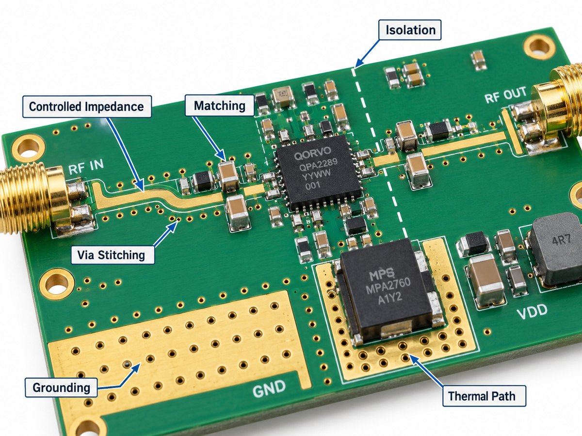
A motor controller that regulates speed over a local feedback loop is an embedded system. Add a network interface, device identity, secure update path, gateway or cloud connection, and remote data service, and the product may become part of an IoT system. The extra connectivity changes power demand, memory use, cybersecurity planning, radio or Ethernet layout, regulatory work, and lifecycle support.

Embedded controller PCB installed in an industrial automation cabinet

How Does Embedded Software Control the Hardware?

Embedded software configures the processor and peripherals, reads inputs, schedules work, handles faults, and drives outputs. It is usually closer to the hardware than desktop application software because register settings, interrupts, timing, memory limits, and electrical interfaces directly affect behavior.

A small controller may use bare-metal firmware with a main loop and interrupt service routines. A more complex design may use a real-time operating system to schedule tasks and manage communication, or embedded Linux when the product needs extensive networking, storage, graphics, or application frameworks. The most suitable option depends on timing, memory, boot time, update strategy, security, maintainability, and available engineering resources.

Which PCB Design Decisions Matter in Embedded Hardware?

PCB layout turns the system architecture into physical hardware, so electrical, thermal, mechanical, and test requirements must be resolved together rather than after routing.

  • Power integrity: Place regulators, bulk capacitance, and high-frequency decoupling around the actual load and current path.
  • Ground and return paths: Give clocks, buses, converters, radios, and analog signals continuous, controlled return paths.
  • Signal integrity: Treat fast edge rates, not only clock frequency, as the trigger for impedance, termination, crosstalk, and via-stub review.
  • Analog and digital interaction: Control noisy switching currents before separating areas mechanically or cutting ground planes.
  • Protection and interfaces: Put ESD, surge, filtering, isolation, and level translation where the external connection enters the board.
  • Thermal behavior: Estimate loss in processors, regulators, drivers, and power devices, then provide copper area, thermal vias, airflow, or a heatsink path as needed.
  • Debug and production access: Reserve programming headers or pads, test points, boot controls, and serial diagnostics before the enclosure removes access.
  • Manufacturability: Review package geometry, component spacing, assembly side, panelization, fiducials, inspection access, and component lifecycle before release.

A control board article can help translate these system requirements into board functions, while our embedded boards guide covers the board-level platform in more detail.

How Should an Embedded System Be Tested?

Testing should prove both that the PCB was assembled correctly and that the complete hardware-software system performs its intended function. A visually perfect board can still fail because of power sequencing, firmware, timing, communication, sensor calibration, or interaction with the enclosure.
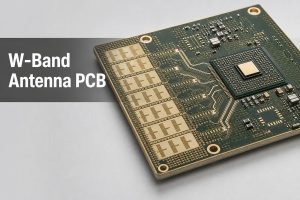
  1. Pre-power checks: Inspect polarity, orientation, soldering, resistance to ground, and expected rail isolation.
  2. Controlled power-up: Use current limits and verify each rail, reset state, clock, and boot condition.
  3. Programming and interface checks: Confirm the debug path, firmware image, memory, communication ports, and peripheral identification.
  4. Functional tests: Apply representative inputs and confirm outputs, timing, fault handling, and recovery behavior.
  5. Production coverage: Combine appropriate inspection and electrical methods, which may include AOI, X-ray for hidden joints, in-circuit or flying-probe checks, and a product-specific functional fixture.
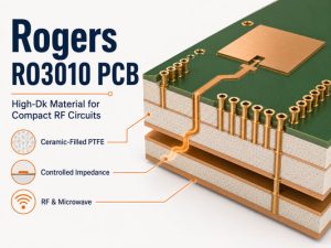
  6. System validation: Verify the assembled product under the environmental, electrical, mechanical, safety, EMC, and cybersecurity requirements that apply to its market and use case.

Engineer probing an embedded system PCB during oscilloscope testing

For a closer look at choosing coverage rather than relying on a single inspection step, see our guide to PCB assembly testing services.

FAQ About Embedded Systems

What are embedded systems examples? Common examples include appliance controllers, smart sensors, motor drives, vehicle control modules, printers, cameras, access-control devices, routers, portable instruments, and industrial monitoring equipment. The embedded computer is usually one subsystem inside the finished product.

What are embedded systems and why are they important? Embedded systems give products local sensing, decision-making, communication, and control. They can respond without sending every action to a remote computer, and their hardware can be tailored to the product’s power, size, cost, and environmental limits.

What are embedded systems in IoT? In an IoT product, the embedded system reads sensors, controls local functions, manages a communication interface, and prepares data for a gateway or cloud service. Secure identity, updates, data protection, and loss-of-network behavior become part of the design.

What are embedded systems in electronics? They are electronic assemblies that combine processing, memory, power, I/O, and firmware to perform a defined function. The processor may be a microcontroller, microprocessor, SoC, DSP, or FPGA, depending on the workload.

Do all embedded systems use an RTOS? No. A simple controller can run a loop, state machine, and interrupts without an operating system. An RTOS becomes useful when several time-sensitive tasks, communication stacks, resource sharing, or maintainable scheduling justify the added software layer.

Is a Raspberry Pi an embedded system? It can be. The board is a general development platform, but it becomes part of an embedded system when it is integrated into a product with a fixed function, controlled software image, defined interfaces, and a product-level validation plan.

How Can EBest Circuit Help Turn an Embedded Design into Hardware?

The practical answer to what are embedded systems is that hardware and software must work as one product. At EBest Circuit, we support PCB design review, prototyping, PCB fabrication, component sourcing, PCBA assembly, and testing for teams turning embedded designs into physical assemblies.

For an engineering review or quotation, send your Gerber files, BOM, quantity, assembly drawings, and available programming or functional-test requirements to sales@bestpcbs.com. We can review the manufacturing package and help identify PCB or assembly details that should be resolved before production.

You may also like

High-Speed PCB Materials: Dk, Df, FR-4 and Low-Loss Selection Guide

September 8th, 2026

High-speed PCB materials should be selected by insertion-loss budget, Df, Dk stability, copper roughness, dielectric thickness, glass weave, impedance target and manufacturing availability. FR-4 may still work for shorter channels, while low-loss laminates are better for longer or tighter-margin SerDes links.

That does not mean every high-speed PCB needs an ultra-low-loss laminate. Standard or enhanced FR-4 can still work well for shorter channels with enough margin. Low-loss materials become more useful when longer SerDes links, dense routing, multiple vias, or tighter insertion-loss targets leave less room for error.

High-speed PCB materials showing Dk, Df, copper roughness, glass weave, impedance and multilayer PCB stackup

What Are High-Speed PCB Materials?

High-speed PCB materials are laminate and dielectric systems chosen for predictable electrical behavior at higher signal frequencies and edge rates.

They may include:

  • standard FR-4
  • enhanced FR-4
  • mid-loss epoxy laminates
  • low-loss and very-low-loss laminates
  • hydrocarbon ceramic materials
  • PTFE-based materials

A high-speed PCB is not defined only by clock frequency. Fast rise and fall times can make a trace behave like a transmission line even when the nominal clock looks relatively low.

Once trace length becomes electrically significant, the design must account for:

  • controlled impedance
  • reflections
  • dielectric loss
  • conductor loss
  • return-path continuity
  • timing skew

This is why specifying only “FR-4” or “low-loss material” is rarely enough. The laminate grade, dielectric thickness, copper type, and stackup should be reviewed together.

Which PCB Material Properties Matter Most at High Speed?

For most high-speed digital boards, the most useful properties to review are Df, Dk stability, copper roughness, and dielectric construction.

Property Why It Matters
Df Influences dielectric loss and insertion loss
Dk Affects impedance and propagation delay
Dk stability Helps maintain impedance and timing consistency
Copper roughness Increases conductor loss at high frequency
Dielectric thickness Determines controlled-impedance geometry
Glass weave Can contribute to differential skew
Tg / Td Affects thermal reliability
CTE Influences via and plated-hole reliability
Moisture absorption Can change electrical behavior
CAF resistance Matters for dense spacing and long-term reliability

Dissipation factor, or Df, is often one of the first parameters engineers compare. Standard FR-4 may fall roughly in the 0.015–0.025 range, while low-loss laminates can be below 0.010 and very-low-loss systems may fall below 0.005.

Dielectric constant, or Dk, affects impedance and signal velocity. A lower Dk can be useful, but consistency is often more important than simply choosing the lowest available value.

A material change may require new:

  • trace widths
  • differential spacing
  • dielectric thicknesses
  • copper thickness assumptions

That is why impedance calculations should be tied to the actual production stackup.

What Types of PCB Dielectric Materials Are Used for High-Speed Applications?

PCB dielectric materials for high-speed applications usually fall into four practical groups.

A PCB material for RF applications may also suit some high-speed digital channels, but the final choice must match the channel loss, impedance, thermal, and fabrication requirements.

Material Family Typical Use Relative Loss Manufacturing Consideration
Standard / enhanced FR-4 General digital, shorter high-speed links Moderate Widely available and economical
Mid-/low-loss epoxy Multi-gigabit digital systems Low Often processed similarly to FR-4
Hydrocarbon ceramic High-speed digital, RF, mixed-signal Low to very low Requires closer stackup control
PTFE-based material RF, microwave, mmWave, very-low-loss channels Very low Requires more specialized fabrication
Comparison of FR-4, low-loss epoxy, hydrocarbon ceramic and PTFE PCB dielectric materials for high-speed applications

Standard and enhanced FR-4 remain useful because they are economical, widely stocked, and familiar to most PCB manufacturers. Their main limitation in high-speed work is higher loss over long channels.

Low-loss epoxy laminates are a common next step for networking, telecom, data-center, and AI hardware. They reduce dielectric loss without always introducing the fabrication complexity associated with more specialized RF materials.

Hydrocarbon ceramic materials suit designs that need low loss, stable electrical properties, or a mix of high-speed digital and RF functions.

PTFE-based materials offer very low loss, but they usually need tighter process control and are best reserved for applications that genuinely require them.

Material family should be selected first. The exact product grade can then be chosen according to electrical requirements, available constructions, and supplier availability.

How Do FR-4 and Low-Loss PCB Materials Compare?

The biggest difference between FR-4 and low-loss laminates is the amount of channel loss they introduce over distance and frequency.

Comparison Standard FR-4 Low-Loss Laminate
Dielectric loss Higher Lower
Typical Df Often ~0.015–0.025 Commonly below ~0.010
Long high-speed channels More limited Better suited
Material cost Lower Higher
Availability Very broad Grade-dependent
Fabrication familiarity Excellent Usually good
Stackup flexibility High Depends on stocked constructions
Insertion-loss margin Lower Higher
Best fit Shorter, cost-sensitive channels Longer, loss-sensitive channels
FR-4 versus low-loss PCB materials comparison for cost, loss, channel length and signal margin

The laminate is only part of the channel. Copper profile, routing length, vias, and connectors can change the result significantly.

For example, a low-Df laminate paired with rough copper may not perform as well as expected. An enhanced FR-4 system with smoother copper and shorter routes may be perfectly adequate.

So material selection should be based on total channel performance rather than one datasheet value.

When Is FR-4 Still Suitable for a High-Speed PCB?

FR-4 is still suitable when the complete interconnect remains inside the required loss, timing, and impedance limits.

There is no universal point where FR-4 suddenly becomes unusable.

FR-4 is often a reasonable choice when:

  • high-speed traces are relatively short
  • insertion-loss margin is comfortable
  • the channel contains few connectors or via transitions
  • impedance can be achieved with practical trace geometry
  • the selected FR-4 grade has acceptable Df and Dk stability
  • project cost is sensitive to material upgrades

Moving to a lower-loss laminate becomes more attractive when the design has:

  • longer routed channels
  • higher SerDes data rates
  • more connectors
  • more via transitions
  • tight eye-diagram margin
  • backplane routing
  • higher routing density
  • stricter insertion-loss targets

A more expensive laminate will not correct a poor interconnect structure. If the main problem is a long via stub, an interrupted return path, or a badly designed connector transition, the geometry still needs to be fixed.

How Do Dk, Df, Copper Roughness and Glass Weave Affect Signal Integrity?

These factors influence different parts of the channel.

High-speed PCB signal integrity factors including Dk, Df, copper roughness and glass weave

Df affects dielectric loss. Part of the signal energy is dissipated in the dielectric as the signal propagates. Higher Df generally means more attenuation, especially over longer traces and at higher frequencies.

Dk affects impedance and signal velocity. Changes in Dk alter characteristic impedance, propagation delay, and the trace dimensions needed to meet a target such as 50 Ω or 100 Ω differential.

Copper roughness affects conductor loss. At high frequency, current flows close to the conductor surface because of skin effect. Rougher copper increases the effective path length and therefore resistance.

For longer channels, designers often review whether the stackup uses:

  • standard copper
  • reverse-treated copper
  • low-profile copper
  • very-low-profile copper

Glass weave can contribute to skew. Glass bundles and resin-rich areas do not have identical dielectric properties. If the two traces in a differential pair see different local material environments, propagation delay can differ.

Common mitigation methods include:

  • choosing suitable glass styles
  • routing pairs at an angle to the weave
  • using resin-rich constructions where appropriate
  • avoiding unnecessarily long parallel runs aligned with the weave

For demanding links, these details can matter as much as the headline Dk and Df numbers.

How Do You Choose the Right High-Speed PCB Material?

Start with the interface and channel requirement rather than choosing a laminate brand first.

High-speed PCB material selection process based on interface, channel length, loss budget, Dk, Df, copper, stackup and material availability

A practical selection process is:

  1. Identify the interface and data rate. Define whether the board uses PCIe, Ethernet, USB, HDMI, DDR, proprietary SerDes, RF, or a combination.
  2. Estimate the channel length. Include PCB traces, vias, connectors, cables, and backplane sections where applicable.
  3. Define the insertion-loss budget. Determine how much attenuation the transmitter and receiver can tolerate.
  4. Compare Dk and Df at relevant frequencies. Avoid comparing datasheet values measured with different methods without understanding the difference.
  5. Review copper foil type. Smoother copper can reduce conductor loss on long or high-frequency channels.
  6. Check dielectric thickness and glass style. These affect impedance geometry and differential skew.
  7. Confirm the production stackup. Make sure the required cores, prepregs, and copper options are actually available.
  8. Balance margin against cost. Use the material performance the channel requires rather than automatically specifying the lowest-loss laminate available.

For high-layer-count boards, a hybrid stackup may also be worth considering. Low-loss material can be used on critical signal layers while more conventional materials are used elsewhere, provided the laminate systems are compatible and the construction can be manufactured reliably.

Which High Speed PCB Design Guidelines Depend on Material Selection?

Several high-speed PCB design decisions depend directly on the material and stackup.

Controlled impedance is the most obvious example. A 50 Ω trace does not have one standard width. Its geometry depends on:

  • dielectric constant
  • dielectric thickness
  • copper thickness
  • solder mask
  • reference-plane position
  • whether the trace is microstrip or stripline

Material selection also affects differential-pair geometry and routing space under dense BGAs.

Via structures can also change with channel requirements. Long through-hole stubs may add resonances and loss, so designs may use:

  • blind vias
  • buried vias
  • backdrilling
  • controlled-depth drilling

Reference-plane continuity should remain intact. Crossing a split plane or poorly defined return path can create a larger signal-integrity problem than the laminate itself.

Other material-dependent checks include:

  • stackup symmetry
  • dielectric thickness tolerance
  • resin content
  • copper profile
  • impedance tolerance
  • trace-width manufacturability
  • lamination compatibility

High-speed layout and stackup development should therefore happen together rather than as separate steps.

What Should You Confirm With a PCB Manufacturer Before Finalizing the Material?

Before freezing the layout, confirm the actual production construction with the PCB manufacturer.

At minimum, verify:

  • exact laminate grade or approved equivalent
  • core and prepreg construction
  • finished dielectric thickness
  • copper foil type
  • starting and finished copper thickness
  • Dk and Df reference values
  • test frequency and measurement method
  • glass style where relevant
  • target impedance and tolerance
  • permitted material substitutions
  • material availability
  • hybrid-material compatibility
  • prototype and production lead time

For controlled-impedance boards, stackup review before layout release is especially useful. A change in dielectric thickness or copper thickness can require new trace widths or differential spacing.

EBest Circuit supports high-speed PCB fabrication and PCBA projects involving controlled impedance, multilayer stackups, HDI structures, low-loss laminates, RF materials, and mixed-material constructions. Our engineering team can review the proposed stackup, material availability, impedance requirements, via structure, copper specification, and manufacturing data before production.

Frequently Asked Questions About High-Speed PCB Materials

What is the best material for a high-speed PCB?

The best PCB material for high speed applications is the material that meets the channel loss and impedance targets without unnecessary cost or fabrication risk. The correct choice depends on data rate, trace length, insertion-loss budget, stackup, copper profile, operating environment, manufacturing requirements, and cost. Shorter channels may work well with enhanced FR-4, while longer loss-sensitive channels can justify low-loss or very-low-loss laminates.

Is FR-4 suitable for high-speed PCB design?

Yes. FR-4 can still be suitable for high-speed digital designs when channel length and insertion loss remain within the interface budget. The decision should be based on channel simulation or loss analysis rather than a fixed frequency threshold.

What Dk is suitable for a high-speed PCB?

Many high-speed PCB materials have Dk values roughly between 3 and 4.5, but the exact value is less important than predictable electrical behavior and a stackup that supports the required impedance geometry. Dk should also be compared using the same test method and frequency where possible.

Is lower Df always better for high-speed PCBs?

Electrically, lower Df generally reduces dielectric loss, but the lowest-Df material is not automatically the best commercial choice. Material cost, copper profile, availability, fabrication complexity, and actual channel length should also be considered.

When should I use a low-loss PCB laminate?

Low-loss material becomes more valuable when longer traces, higher SerDes rates, multiple connectors or vias, tighter eye margins, or demanding insertion-loss targets make standard FR-4 difficult to use reliably. The transition should be based on channel performance rather than a simple GHz threshold.

What information should I give my PCB manufacturer when selecting a high-speed material?

Provide the proposed stackup, laminate preference, dielectric thickness, copper weight, target impedance, impedance tolerance, interface type, expected data rate, critical trace lengths, via structure, and any insertion-loss requirement. If a specific material grade is mandatory, state whether substitutions are allowed.

If you are preparing a high-speed PCB or PCBA project, send your Gerber files, stackup, BOM, controlled-impedance requirements, and material specifications to sales@bestpcbs.com. EBest Circuit can review the material system, dielectric construction, copper profile, impedance targets, via structure, and manufacturing requirements before production, helping you avoid unnecessary material cost while protecting signal-integrity margin.

You may also like

PCB Delamination in High-End Materials: Causes and Prevention

September 7th, 2026

PCB delamination is the loss of adhesion between layers or interfaces inside a printed circuit board. In a high-end multilayer PCB, the separation may occur between copper and resin, within the dielectric system, around glass reinforcement, or near a plated hole. It may remain hidden until lamination, lead-free assembly, rework, or field heating adds enough pressure and stress to open the weak interface.

Advanced material does not automatically mean a board is more likely to delaminate. The risk rises when low-loss resin systems, smoother copper, thin dielectrics, dense copper patterns, hybrid materials, repeated lamination cycles, and high-temperature assembly are combined without a matched process window. Preventing the defect requires control of the complete material-and-process system, not a single datasheet value.

High-end multilayer PCB cross section showing moisture, thermal stress, and a weak interface causing delamination

What Is PCB Delamination in High-End Materials?

PCB delamination in high-end materials is an interfacial or cohesive bond failure that separates layers which should remain permanently joined. The defect can be local or extensive and may appear as an internal void, a lifted copper feature, a surface blister, or separation near a via or board edge.

Delamination should not be confused with every pale or fibrous mark visible in a laminate. Measling and crazing describe different resin-glass conditions, while a blister is a localized raised area that may result from internal separation or trapped volatiles. A confirmed disposition should identify where the separation occurred and whether it interrupts a conductor, reduces insulation spacing, exposes a path for moisture, or weakens the structure.

Observed Condition Likely Location Why It Matters
Surface blister Solder mask, copper-to-dielectric, or near-surface laminate May indicate trapped moisture, poor adhesion, or contamination
Internal planar separation Core-prepreg or copper-resin interface Can expand during thermal cycling and affect insulation or signal paths
Separation near a via Resin, copper interface, or glass bundle beside the barrel May combine with Z-axis stress and threaten via reliability
Edge separation Routed edge or exposed laminate interface Can admit moisture and propagate under later heating

Why Can Advanced PCB Materials Delaminate?

Advanced PCB materials delaminate when the stress applied to an interface exceeds the bond strength available at that location. The initiating weakness can come from the material, storage, surface preparation, stackup design, lamination process, drilling and plating, assembly heating, or rework.

High-end constructions can make the margin narrower for several reasons:

  • More interfaces: high layer counts create more bond lines and more opportunities for local contamination or incomplete wetting.
  • Thin dielectrics and dense copper: resin must fill narrow spaces and compensate for uneven copper distribution without starving another area.
  • Smoother copper: low-profile foil reduces conductor loss, but the selected treatment and resin system must still provide reliable adhesion.
  • Multiple lamination cycles: sequential-build HDI boards expose earlier layers to repeated heat and pressure.
  • Hybrid material systems: different resins, glass styles, copper treatments, and coefficients of thermal expansion may not move together during heating.
  • Higher assembly temperature: lead-free reflow and repeated rework can consume the thermal margin of a weak bond.

The main PCB delamination causes are therefore interactive. Moisture alone may not damage a well-bonded construction, and one thermal excursion may not open a dry board. Moisture, a weak interface, and rapid heating together are far more dangerous.

How Do Moisture and Thermal Shock Start Delamination?

Moisture and thermal shock start delamination when absorbed water expands, vaporizes, or changes the mechanical behavior of the laminate faster than pressure can dissipate. During reflow or rework, vapor pressure acts on the weakest internal interface while copper, glass, and resin expand at different rates.

An IPC technical paper on moisture in PCB laminates reported that absorbed moisture reduced time-to-delamination performance for several evaluated materials. The same work explains that moisture affects swelling and Z-axis expansion. This supports a practical rule: thermal robustness must be evaluated in the conditioned state that represents handling and assembly, not only on a dry datasheet specimen.

Before-and-after PCB cross section showing absorbed moisture becoming vapor pressure during reflow

Common exposure paths include:

  • unsealed laminate, prepreg, or finished boards stored in humid conditions;
  • a long floor-life interval before assembly;
  • aqueous processing followed by inadequate drying;
  • rapid heating or an excessive reflow peak;
  • multiple reflow, wave-solder, selective-solder, or hand-rework cycles;
  • baking followed by poor packaging or renewed moisture exposure.

Baking can reduce moisture when the material and finish allow it, but it cannot restore a contaminated interface, replace missing resin, or repair an already separated bond. The bake condition must be approved for the board construction and surface finish.

How Do Lamination Parameters and Resin Flow Cause Weak Bonds?

Lamination parameters and resin flow cause weak bonds when the resin does not fully wet, fill, cure, and consolidate every interface in the stackup. The press cycle must match the actual resin system, panel mass, copper distribution, dielectric thickness, and number of layers.

  • Insufficient flow can leave voids, glass stop, or resin-starved areas around heavy or dense copper.
  • Excessive flow can squeeze resin away from a critical bond line and change finished dielectric thickness.
  • Poor vacuum can leave trapped air or volatiles in a stack that appears flat externally.
  • Incorrect heat-up rate can move the resin through its workable viscosity range before pressure and flow are balanced.
  • Inadequate pressure may prevent full consolidation; excessive pressure may worsen resin loss or dimensional movement.
  • Incomplete cure reduces thermal and chemical resistance, while an unsuitable cycle can embrittle or over-stress the system.

Prepreg selection must also provide enough resin to fill the designed copper topography. A technically advanced low-loss laminate can still fail if the chosen prepreg construction cannot fill a dense copper area without starving an adjacent region.

Why Do Surface Preparation and Copper Profile Matter?

Surface preparation and copper profile matter because adhesion depends on both chemical compatibility and the physical condition of the bonding surface. Oxidation, fingerprints, release residue, cleaning chemistry, dust, or excessive delay after treatment can reduce the bond strength before the stack enters the press.

High-speed boards often use smoother copper to reduce conductor loss. That does not mean smooth copper is unsuitable, but it leaves less room for an uncontrolled bonding process. The foil treatment, oxide alternative, resin chemistry, handling method, and lamination cycle must be qualified together.

PCB microsection comparison showing a good bond, low resin flow, and a contaminated interface

A useful failure analysis asks whether the separation is adhesive, at the copper-resin boundary, or cohesive, within the resin or reinforced dielectric. That distinction guides the corrective action. Increasing press pressure will not correct surface contamination, and extra cleaning will not fix a resin-volume shortage.

How Do Hybrid Materials and Repeated Lamination Add Risk?

Hybrid materials and repeated lamination add risk by combining interfaces with different thermal expansion, cure behavior, surface treatment, and thermal history. The construction may be electrically attractive but still require a narrower manufacturing window than a homogeneous stackup.

Before releasing a hybrid or sequential-lamination design, the fabricator should review:

  • resin-system compatibility and supplier processing guidance;
  • X-Y and Z-axis expansion through the expected thermal range;
  • Tg, decomposition temperature, and time-to-delamination data;
  • copper treatment and interlaminar adhesion;
  • prepreg flow and fill across copper-density transitions;
  • the total number of lamination and assembly heat cycles;
  • drill, desmear, plasma, and plating chemistry compatibility.

Tg alone is not a sufficient selection rule. An IPC comparison of laminate thermal properties showed that time-to-delamination behavior did not simply follow Tg; decomposition temperature and the material system also mattered. The released requirement should therefore reflect the real thermal profile and reliability target.

What Does Delamination Look Like and How Is It Confirmed?

Delamination can look like a surface bubble, pale patch, lifted pad area, edge split, or local swelling, but internal separation may have no reliable external sign. PCB delamination images are useful for screening only; lighting, solder-mask color, glass weave, measling, and machining marks can make different defects look similar.

Confirmation should use methods appropriate to the suspected location:

  • Visual and dimensional inspection: identifies blistering, bow, twist, edge separation, or surface change.
  • Scanning acoustic microscopy: can map planar internal separations when equipment and board geometry allow.
  • Microsection: destructively reveals the bond line, void, resin condition, copper interface, and nearby via structure.
  • Thermal stress or simulated reflow: checks whether a latent weakness opens under the intended assembly exposure.
  • TMA time-to-delamination: characterizes laminate response at a specified test temperature; IPC lists TM-650 method 2.4.24.1 for this measurement.
  • Electrical and reliability testing: determines whether the defect has affected insulation, continuity, impedance, or via performance.

A PCB delamination cross section should be taken through the actual indication whenever possible. A clean section from a distant coupon cannot explain a localized production defect.

Can PCB Delamination Be Repaired?

PCB delamination repair is usually not acceptable for an internal structural separation in a high-reliability multilayer board. Injecting adhesive, pressing a blister flat, or baking the board may hide the symptom without restoring the qualified dielectric spacing, bond integrity, insulation performance, or long-term thermal reliability.

A limited external defect may sometimes receive an engineering disposition if the applicable drawing, acceptance standard, customer, and reliability assessment permit it. That decision should document the location, size, affected conductors, insulation distance, test evidence, and intended service environment. It should not be treated as a general repair method.

For confirmed internal delamination, the safer corrective path is normally to quarantine the lot, determine the failure interface, verify the extent, correct the root cause, and rebuild affected product. Rework without root-cause evidence can convert a visible manufacturing escape into a field failure.

How Should Fabricators Improve a Delamination Process?

Fabricators should improve a delamination process by linking the failure location to the process step that created the weak interface. Corrective action should be evidence-based and verified with a controlled build.

Confirmed Cause Immediate Improvement Verification
Moisture before thermal exposure Restore dry storage, packaging, exposure control, and an approved bake process Moisture review plus representative reflow or thermal stress
Resin starvation or glass stop Adjust prepreg construction, copper balancing, pressure, vacuum, and heat-up profile Microsections across high- and low-copper-density areas
Contaminated or degraded surface Correct cleaning, surface treatment, rinsing, drying, and hold-time control Bond assessment, peel testing where applicable, and thermal exposure
Hybrid-material mismatch Reassess compatibility, CTE, cure, thickness, and thermal history Qualification panels using the production stackup
Assembly or rework overheating Correct the thermal profile and limit cumulative excursions Profile records and post-process inspection

The verification build should use production-intent material lots, copper distribution, panel format, lamination equipment, and assembly exposure. A laboratory coupon that removes the difficult geometry may prove the resin can bond, but not that the released PCB can be manufactured consistently.

How Can Designers and Buyers Prevent PCB Delamination?

Designers and buyers prevent PCB delamination by defining the material system, thermal exposure, and acceptance evidence before the quotation is locked. Early collaboration gives the fabricator room to adjust prepreg, copper balance, and the lamination sequence without changing finished electrical requirements.

  1. Share the real thermal history. Include all lamination, reflow, wave, selective-solder, press-fit, coating cure, and expected rework cycles.
  2. Approve exact materials and alternates. Do not authorize substitution by a broad “equivalent high-Tg” note.
  3. Review copper balance and resin demand. Large copper-free zones beside dense planes require deliberate fill planning.
  4. Set storage and floor-life controls. Define packaging, humidity exposure, resealing, and any allowed bake process.
  5. Use production-intent prototypes. Qualify the same material family, stackup, and critical process sequence planned for volume.
  6. Specify evidence. Require the appropriate microsections, thermal stress, reflow simulation, coupons, traceability, and change notification.

For designs where thin dielectrics and sequential lamination raise the risk, our HDI PCB fabrication guide explains the build-up context. For electrical geometry that must remain stable after material or thickness changes, see our impedance control PCB guide.

What Should Be Included in a Delamination Control Plan?

A delamination control plan should translate the risk into measurable incoming, fabrication, assembly, and verification controls. At minimum, it should record:

  • approved laminate, prepreg, copper, and surface-treatment combinations;
  • material storage, packaging, exposure, and bake conditions;
  • prepreg resin content and fill assumptions for the released copper pattern;
  • surface preparation, hold time, and contamination controls;
  • vacuum, pressure, temperature, heat-up, dwell, and cooling windows;
  • sequential lamination and cumulative assembly heat cycles;
  • inspection sampling locations and acceptance criteria;
  • material-lot and process traceability;
  • the response plan for blistering, separation, or an abnormal microsection.
Keep dry, prepare, laminate, and verify workflow for preventing PCB delamination

The plan should also define who can approve a material, stackup, or process change. If availability forces a substitution, production should pause at the approval gate rather than silently consume a different construction.

Frequently Asked Questions About PCB Delamination

What causes PCB delamination?

The immediate cause is stress exceeding local bond strength. Common contributors include moisture, rapid heating, inadequate resin flow, incomplete cure, contaminated surfaces, incompatible materials, repeated thermal cycles, and excessive rework.

Does a higher Tg prevent delamination?

No. Tg is important, but it does not describe moisture behavior, decomposition, time-to-delamination, copper adhesion, resin flow, or the quality of the fabricated bond line.

Can baking fix an already delaminated PCB?

No. An approved bake may remove moisture before heating, but it does not restore an interface that has already separated or correct contamination and resin starvation.

Why does delamination appear after reflow instead of during PCB fabrication?

A weak interface may remain closed and invisible after lamination. Reflow adds rapid thermal expansion and vapor pressure, exposing the latent defect.

Can AOI or X-ray always find internal delamination?

No. AOI examines visible surfaces, and standard transmission X-ray may not clearly reveal a planar separation. Acoustic imaging, targeted microsectioning, and thermal verification are often more informative.

Are low-loss PCB materials inherently prone to delamination?

No. They require a compatible copper treatment, prepreg construction, lamination cycle, handling method, and assembly profile. A qualified process can produce reliable low-loss multilayer boards.

How Can EBest Circuit Help Prevent PCB Delamination?

At EBest Circuit, we can review your Gerber files, stackup, laminate and prepreg callouts, copper distribution, via structure, target impedance, assembly profile, quantity, and inspection requirements before fabrication. We use those inputs to identify moisture, resin-fill, material-interface, and thermal-cycle risks that should be closed before production.

Send the released data and your reliability requirements to sales@bestpcbs.com. We will return the engineering questions, proposed stackup controls, and verification items needed for a manufacturable high-end multilayer PCB.

You may also like

Electromagnetic Shielding: Materials, Effectiveness, and PCB Design

September 7th, 2026

Electromagnetic shielding uses conductive or magnetic barriers to reduce unwanted electromagnetic energy entering or leaving a circuit. Effective shielding is not simply a metal cover: the material, frequency, seams, apertures, cable entries, grounding path, PCB layout, and test method must work as one system.

For PCB teams, the best result usually comes from reducing noise at its source, controlling the coupling path, protecting the sensitive circuit, and then adding a shield where residual emissions or susceptibility still require it. This guide explains how to make those decisions without treating shielding as a late-stage patch.

PCB assembly with a grounded metal shield controlling electromagnetic fields

What Is Electromagnetic Shielding?

Electromagnetic shielding is a barrier that attenuates electric, magnetic, or electromagnetic fields between a source and a protected region. In electronics, it helps limit radiated emissions from noisy circuits and improves immunity when sensitive circuits operate near motors, switch-mode power supplies, radios, cables, or fast digital interfaces.

A shield may surround an entire product, cover one PCB area, wrap a cable, close an enclosure seam, or form a conductive layer in a flexible circuit. The correct structure depends on the problem frequency and coupling mechanism. A thin conductive shield can perform well against high-frequency electric fields, while low-frequency magnetic fields may require high-permeability material and a different geometry.

How Does Electromagnetic Shielding Work?

Electromagnetic shielding works mainly through reflection and absorption, with additional internal reflections occurring inside thin or layered materials. Conductive materials support surface currents that oppose an incident field, while magnetic materials can provide a lower-reluctance path for magnetic flux.

  • Reflection: impedance changes at the shield surface redirect part of the incident energy.
  • Absorption: energy decays as currents flow through a lossy conductive or magnetic material.
  • Multiple reflection: energy can reflect between material boundaries, especially in thin, porous, or layered shields.

This is the practical core of electromagnetic shielding theory and applications: performance depends on field type, frequency, material properties, thickness, distance from the source, and electrical continuity. A material data sheet alone cannot predict the finished enclosure or PCB assembly.

Diagram showing reflection and absorption of electromagnetic energy at a conductive shield

Which Electromagnetic Shielding Materials Are Used?

The most useful electromagnetic shielding materials are chosen for conductivity, magnetic permeability, corrosion behavior, mechanical form, solderability, weight, and cost. No material is universally best across all frequencies and product structures.

Material or Structure Main Strength Common Use Main Limitation
Copper High conductivity and solderability Foils, tapes, PCB planes, cable shields Weight, cost, and galvanic compatibility
Aluminum Good conductivity at low weight Enclosures, foil, covers Oxide layer and joining method need attention
Tin-plated steel Formability, solderability, and economical construction Board-level shield cans Greater weight than aluminum
Nickel silver Corrosion resistance and practical shield-can forming Removable and soldered PCB shields Higher material cost than basic steel
High-permeability alloy Redirects low-frequency magnetic flux Transformers, sensors, magnetic-field control Forming and mechanical stress can affect performance
Conductive elastomer or fabric Maintains electrical contact across joints Gaskets, doors, seams, serviceable covers Compression, aging, plating compatibility, and contact resistance

Material selection must include the surrounding metals and environment. Dissimilar metals, moisture, salt, coatings, and repeated opening can increase contact resistance or corrosion risk. For a shield can, the solderable finish and mechanical flatness may matter as much as the base metal.

How Is Electromagnetic Shielding Effectiveness Measured?

Electromagnetic shielding effectiveness is the reduction in field level produced by a shield, normally expressed in decibels at a stated frequency and test condition. For electric-field amplitude, 20 dB represents a 10:1 reduction, 40 dB a 100:1 reduction, and 60 dB a 1000:1 reduction.

The number is meaningful only when the test method, frequency range, sample geometry, field type, and fixture are known. ASTM D4935 is commonly used for planar material samples, while IEEE 299 addresses shielding enclosures. A tape sample measured in a laboratory fixture should not be assumed to deliver the same result after it is applied across a painted seam, around a connector, or inside a vented product.

  • Define the required frequency range and field type.
  • Match the test method to the material, enclosure, cable, or finished product.
  • Record apertures, seams, grounding, gasket compression, and cable configuration.
  • Compare data only when the test conditions are reasonably equivalent.

What Is the Difference Between EMI and EMC Shielding?

EMI describes unwanted electromagnetic interference, while EMC describes a product’s ability to operate correctly in its electromagnetic environment without causing unacceptable interference. Shielding is one technique used to improve EMC; it does not replace source suppression, filtering, grounding, return-path control, or compliance testing.

A product can fail because it emits too much noise or because it is too susceptible to an external field. The same enclosure may help both problems, but the coupling paths can differ. Designers should therefore identify the source, path, victim, frequency, operating mode, and cable state before choosing a shield.

Which Shielding Method Fits the Interference Path?

The shielding method should match the dominant path rather than the visible symptom. Radiated noise, conducted noise, cable common-mode current, enclosure leakage, and local component coupling require different controls.

Interference Path Useful Controls Validation Focus
PCB trace or switching loop radiation Smaller loop area, continuous return plane, source filtering, local shield Near-field scan and radiated emissions
Cable common-mode current Connector filtering, 360-degree shield termination, common-mode control Cable-current probe and system configuration
Enclosure seam or aperture leakage Shorter openings, conductive gasket, overlapping joint, reliable bonding Seam scan and enclosure test
Local circuit-to-circuit coupling Placement separation, ground fencing, board-level shield can Victim-node noise and functional immunity
Low-frequency magnetic field Distance, loop orientation, lower source current, high-permeability shield Magnetic probe and operating-current condition

How Should Electromagnetic Shielding Be Applied to PCB Design?

PCB shielding should begin with current-path control, because a metal can cannot correct every layout problem. Keep high di/dt loops compact, place decoupling close to device pins, use continuous reference planes, and prevent fast return currents from crossing plane splits or connector cutouts.

  1. Identify switching nodes, clocks, RF sections, cables, and sensitive analog circuits.
  2. Minimize source-loop area and keep return paths directly adjacent to critical signals.
  3. Partition noisy and sensitive functions by placement and routing, not by arbitrary ground splitting.
  4. Place stitching vias where return current changes reference or where a shield perimeter needs a low-inductance ground connection.
  5. Define connector-shell, chassis-ground, and signal-ground relationships in the schematic and mechanical design.
  6. Reserve shield-can pads, keep-outs, rework access, and component-height clearance before layout release.

Our guides to PCB ground-plane layout and high-speed PCB design cover the return-path and stackup details that should be resolved before shielding hardware is added.

PCB electromagnetic shielding methods including a shield can, ground plane, via fence, and connector shield

When Should You Use PCB Shielding Cans?

A PCB shielding can is useful when a localized RF, clock, converter, or sensitive receiver section needs additional isolation after the layout and grounding have been optimized. One-piece cans suit permanent coverage, while two-piece frame-and-lid structures improve inspection, tuning, and rework access.

The can needs a continuous, low-inductance connection to the intended ground reference. Its perimeter pads, via stitching, wall height, vent pattern, component clearance, and reflow process must be designed together. Our board-level shielding guide explains can materials, grounding, apertures, and assembly choices in detail.

When Is Electromagnetic Shielding Tape Useful?

Electromagnetic shielding tape is useful for prototypes, seams, cable wrapping, local conductive patches, and surfaces that cannot be soldered directly. Copper, tin-plated copper, and aluminum foil tapes are available with conductive adhesive, but the backing material alone does not guarantee a low-impedance joint.

Check whether the adhesive conducts through its thickness, whether the overlap remains conductive, and whether the tape bonds to bare metal, plating, paint, or plastic. Surface cleanliness, bending radius, oxidation, galvanic compatibility, temperature, humidity, and long-term peeling can all change the result. Tape is excellent for controlled applications and debugging, but it should not hide an unresolved production-design problem.

Why Do Seams, Apertures, and Cables Cause Leakage?

Seams, apertures, and cables cause leakage because they interrupt the shield current or provide a path for common-mode energy to cross the barrier. The longest dimension of a slot is often more important than its total area, so one long opening can leak more than several small holes.

  • Use many small ventilation holes instead of a long slot when airflow permits.
  • Maintain conductive contact around serviceable seams with suitable gaskets or spring fingers.
  • Bond connector shells to the intended chassis or shield reference with a short, wide connection.
  • Filter or shield conductors at the point where they cross the enclosure boundary.
  • Control coatings, paint, anodizing, and contamination at intentional contact surfaces.

The system drawing should state which contacts are intentional. The distinction between board ground, shield ground, chassis, and protective earth is explained in our GND and earth guide.

How Do You Test and Validate an EMI Shield?

An EMI shield is validated by testing the assembled product in representative operating modes, cable configurations, and mechanical conditions. Material certificates and continuity measurements are useful inputs, but they cannot replace a system-level emissions or immunity evaluation.

  1. Establish a baseline: measure the unshielded design or an earlier build under repeatable conditions.
  2. Locate the source: use near-field electric and magnetic probes to identify hot loops, seams, and cables.
  3. Change one variable: add a can, gasket, tape, filter, or grounding change without mixing several unknowns.
  4. Run pre-compliance checks: compare emissions across the relevant frequency range and product modes.
  5. Verify the final assembly: test with production fasteners, covers, coatings, cables, and software states.
  6. Complete required compliance testing: use the standards and limits applicable to the product and destination market.

For U.S. unintentional radiators, FCC guidance points to defined Part 15 measurement procedures; other markets and product categories may require CISPR, IEC, automotive, aerospace, medical, or customer-specific methods. The applicable standard must be identified for the finished product rather than inferred from the PCB alone.

Engineer validating PCB electromagnetic shielding with a near-field probe and test equipment

Frequently Asked Questions About Electromagnetic Shielding

What is the most effective material for electromagnetic shielding?

There is no single most effective material for every case. Copper and aluminum work well for many high-frequency electric-field and plane-wave problems, while high-permeability alloys are more suitable for some low-frequency magnetic fields. The enclosure geometry, seams, apertures, grounding, frequency, corrosion environment, and test method usually determine the finished result.

Does thicker metal always improve shielding?

No. Thickness can improve absorption when it is small relative to the required attenuation, but at high frequency a thin conductive layer may already exceed several skin depths. Leakage through seams, vents, connectors, and poor bonds can then dominate. Increasing wall thickness will not repair an electrically open joint or an unfiltered cable penetration.

Does an EMI shield always need to be grounded?

Not every shield requires a DC earth connection, but most practical PCB and enclosure shields need a controlled low-impedance relationship to the intended reference. The correct connection depends on frequency, safety architecture, cable termination, ESD path, and enclosure design. A long wire that looks grounded at DC may behave inductively at RF.

Can aluminum foil block electromagnetic interference?

Aluminum foil can attenuate some high-frequency electric fields when it forms a continuous enclosure with controlled seams and connections. A loose sheet or incomplete wrap is not equivalent to a qualified shield. Openings, oxide at contact points, cable entry paths, mechanical durability, and the field frequency determine practical effectiveness.

Can shielding fix a poor PCB layout?

Shielding can reduce residual radiated coupling, but it cannot reliably correct every return-path, common-mode, decoupling, or cable-current problem. Source suppression and layout correction usually provide a more stable foundation. Use a shield after the dominant source and coupling path are understood, not as a substitute for that analysis.

How should shielding effectiveness data be compared?

Compare data only when frequency, test method, fixture, sample size, field condition, and assembly details are stated. A planar material test, gasket test, shielded-room test, and finished-device radiated-emissions test answer different questions. Ask for the original test standard and configuration instead of comparing only the highest dB number.

How Can EBest Circuit Support EMI-Sensitive PCB Projects?

At EBest Circuit, we support PCB fabrication and assembly projects that require controlled stackups, continuous reference planes, shield-can landing patterns, via structures, solder-mask openings, and inspection of assembled shielding hardware. The released files should define the intended ground nets and mechanical contacts clearly so production does not have to guess.

Send us your Gerber or ODB++ data, stackup, BOM, shield-can drawing, enclosure interface, quantity, and test requirements. We can review the manufacturability of the PCB and assembly details before production and provide technical support and a quotation at sales@bestpcbs.com.

You may also like