In today’s tech-driven world, creating efficient high speed PCB (Printed Circuit Board) is critical for ensuring devices can handle rapid data transfer without issues. These high speed PCBs are popular in the wireless devices which needs high signal transfer. Crafting high-speed circuits requires careful planning and precise execution to maintain signal quality and overall performance. In this blog, we introduced the basics of high-speed PCB design, offering practical tips and insights into the best materials and techniques for high-frequency applications.
What is a High Speed Circuit PCB?
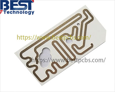
High-speed PCB is a circuit board that can support signal transmission. High-speed signals usually refer to signals with frequencies higher than 50MHz, such as high-speed digital signals, high-speed analog signals, etc. These fast transitions can introduce challenges like signal reflections, electromagnetic interference (EMI), and crosstalk, which can disrupt performance if not properly managed.
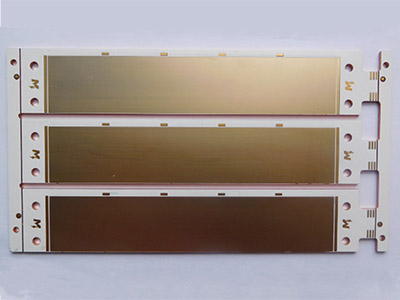
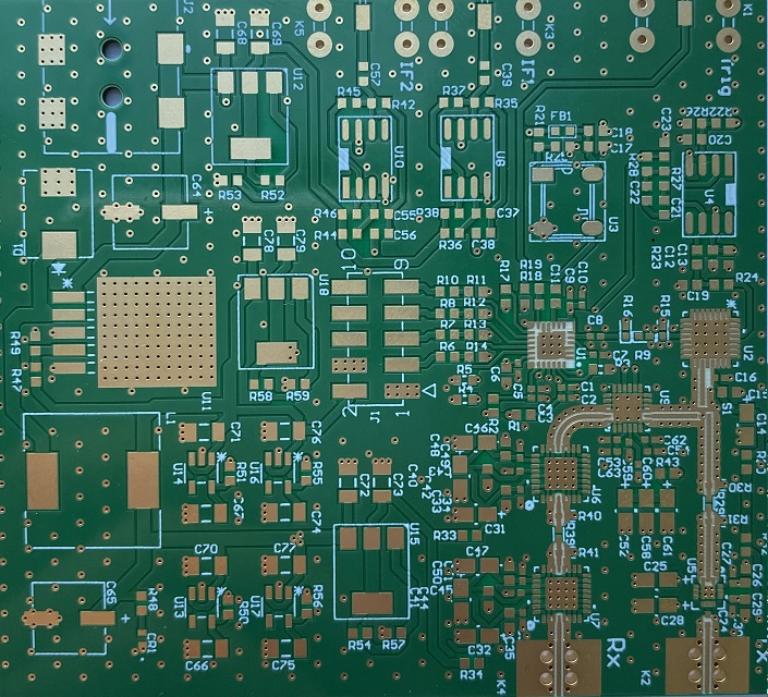
Additionally, these signals will be affected by board materials, layout, wiring and other factors during transmission. Therefore, a specially designed circuit board is required to ensure the integrity and reliability of the signal. Here is a 4 layers high speed PCB for Iradar device with 50ohm single-ended impedance control.
Features of High-Speed PCB
- High frequency
- Low permittivity and low loss factor
- Multilayer design
- Strict impedance control
- High-precision manufacturing
- Low noise characteristic
- High density circuit layout (micro-vias)
- High performance
What is Considered High-Speed PCB Design?
High-speed PCB design focuses on managing the complexities that come with high-frequency signals and fast switching. Key considerations include:
– Signal Integrity: Ensuring signals travel without distortion or loss.
– Power Management: Distributing power effectively to minimize noise and voltage drops.
– Heat Handling: Managing heat from high-speed components to prevent overheating.
– Impedance Matching: Keeping impedance consistent to reduce signal reflections and loss.
– Differential Pair Routing: Reducing EMI and crosstalk by routing complementary signal pairs together.
This type of high speed pcb design requires a solid understanding of electromagnetic principles, advanced simulation tools, and precise manufacturing techniques. For those new to high-speed PCB design, EBest Circuit (Best Technology) offers expert guidance and solutions.
What’s the Best Material for High-Speed PCB Design?
Choosing the right material for high speed pcb is vital for maintaining signal integrity and achieving optimal performance. The material impacts the board’s dielectric constant (Dk), loss tangent, and overall signal quality. Common materials include:
– FR4: Widely used but not ideal for very high frequencies due to higher loss tangent.
– Rogers (RO4000 series): Preferred for high-speed designs thanks to its low dielectric constant and loss tangent.
– Teflon: Excellent for high-frequency applications but more expensive and harder to process.
Selecting the appropriate material ensures the PCB can handle high-speed signals without compromising performance.
Where is the High-Speed PCB Commonly Used in?
High-speed circuit boards are widely used in signal transmission applications, the typical fields are including:
1. Communication equipment – such as 5G base stations, optical fiber communication equipment, etc.
2. Data center – like high-performance computing, storage servers, etc.
3. Consumer electronics in our daily life – high-end smartphones, tablets, gaming devices, etc.
4. Aerospace and military – high speed are always used in high-end devices. For example, radar, navigation systems and other equipment with high reliability requirements.
What is the 3H Rule in High Speed PCB Design?
The 3H rule is a guideline suggesting that signal traces should be spaced at least three times the height of the dielectric (3H) between the signal layer and the adjacent ground or reference layer. This helps minimize crosstalk and maintain signal integrity, particularly for high-speed digital signals with rise times of 1 ns or less. Key aspects include:
– Trace Spacing: Keeping traces apart by at least 3H reduces electromagnetic coupling and interference.
– Signal Integrity: Adequate spacing helps maintain clear signals in high-speed circuits.
– Effectiveness: This rule is especially beneficial for fast digital signals, reducing the risk of crosstalk and interference.
For instance, if the dielectric height between the signal layer and the reference layer is 0.2 mm, traces should be at least 0.6 mm apart to follow the 3H rule.
How to Design a High-Speed Board?
Designing a high-speed PCB involves several strategies to ensure effective signal transmission, power distribution, and minimal EMI. Here’s a step-by-step approach:
Component Placement and Layer Stack-Up
Place high-speed components to minimize signal paths and interference. Group related components to simplify routing. In addition, create a layer stack-up that supports controlled impedance and reduces signal loss. Use ground planes between layers for a return path for high-frequency currents.
Trace Routing and Impedance Control
Keep high-speed traces short and direct, avoiding right-angle bends. Use microstrip or stripline configurations for controlled impedance and minimal noise. For impedance control, calculate and ensure consistent impedance for traces. Use differential pair routing for high-speed signals to reduce EMI and crosstalk.

Power Distribution and EMI Mitigation
Use decoupling capacitors near high-speed components to filter noise and stabilize the power supply. Design a robust power distribution network to minimize impedance and ensure stable voltage. And employ proper grounding and shielding techniques. Route high-speed signals on inner layers between ground planes to reduce EMI and provide a consistent return path.
Simulation and Testing
Use signal integrity analysis tools like SI or PI to simulate the PCB layout, predicting signal behavior and identifying potential issues. Analyze aspects like eye diagrams to assess signal quality.
High-speed PCB design is a complex but rewarding endeavor that ensures your electronics perform efficiently in high-frequency environments. By understanding the fundamentals and applying the right techniques and materials, you can create robust, high-speed boards. EBest Circuit (Best Technology) is here to assist you with expert advice and solutions for your high-speed PCB needs.