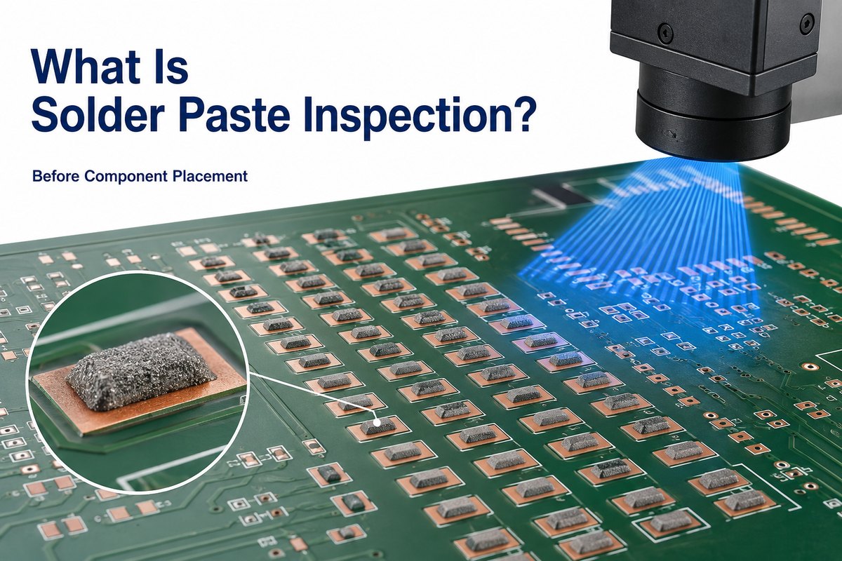
What is solder paste inspection? Solder paste inspection, or SPI, checks the deposits printed onto PCB pads before components are placed. A 3D SPI system measures deposit height and shape to calculate area, volume, and position. These measurements help identify printing problems while the board can still be corrected before placement and reflow.
The useful question is not simply whether the machine displays “pass.” It is whether the inspection program measures the right deposits, uses a suitable reference, and applies limits that have been validated for the assembly. A passing print is one process checkpoint—not proof that every finished solder joint will be reliable.
Where Does SPI Fit in the PCB Assembly Line?
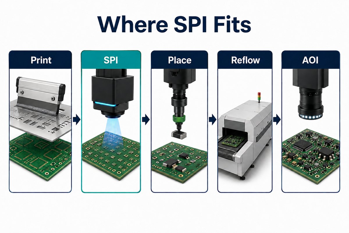
SPI normally sits after stencil printing and before pick-and-place. At this point, the inspection target is the printed paste—not a mounted component or a solidified solder joint.
- Print: a squeegee transfers paste through stencil apertures onto the pads.
- Inspect: SPI checks the deposits against the programmed print requirements.
- Place: components are positioned on accepted prints.
- Reflow: the assembly follows a qualified thermal profile.
- Inspect and test: later checks evaluate placement, accessible joints, hidden features where applicable, and electrical performance.
Finding a printing error early can avoid placing components onto a defective print. It does not remove the need to control placement accuracy, paste condition, reflow, or downstream testing.
Solder Paste Inspection Process
The solder paste inspection process begins with a board-specific program. Accurate machine measurements cannot compensate for an incorrect pad map, reference volume, or revision.
- Load the correct data: match PCB revision, paste-layer data, stencil revision, and component requirements.
- Register the board: use the configured fiducials and board orientation to locate inspection regions.
- Establish the surface reference: identify the local board or pad baseline used for height measurements.
- Measure and classify: compare each deposit with the appropriate target and limits.
- Review exceptions: separate actual print defects from alignment, reference, or recipe errors.
- Record the disposition: release, hold, or clean and reprint under the approved process.
Programming should distinguish solder paste openings from copper and solder mask features. Our explanation of solder mask and solder paste layers covers why these data sets are not interchangeable.
Solder Paste Inspection Parameters
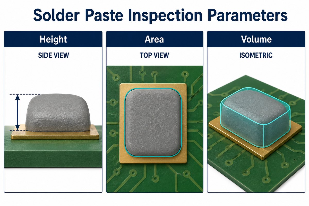
The main solder paste inspection parameters are height, area, volume, and offset. Reading them together is more useful than treating any one number as a complete verdict.
| Parameter | Measurement | Typical units |
| Height | Deposit elevation above the selected reference surface | µm |
| Area | Detected deposit footprint in the board plane | mm² or percentage |
| Volume | Paste volume calculated from measured shape | mm³ or percentage |
| Offset | Deposit displacement from the programmed target | µm in X and Y |
A wide, shallow deposit may have an acceptable-looking footprint but insufficient volume. Conversely, a tall deposit does not necessarily contain the intended total volume if its footprint is small. Offset can also matter even when volume is close to target: the paste must be positioned where the termination and pad need it.
Example—not an acceptance limit: assume a rectangular stencil aperture is 0.30 mm × 0.50 mm in a 0.10 mm thick stencil. Its theoretical aperture volume is 0.015 mm³. A measured deposit of 0.012 mm³ represents 80% transfer efficiency relative to that aperture volume. Whether it is acceptable depends on the validated assembly requirements; 80% is not automatically a pass or fail.
Before interpreting a percentage report, ask what “100%” means. It may refer to theoretical aperture volume or a configured nominal target. Results from different programs are not directly comparable until their reference definitions are aligned.
How Does 3D SPI Measure the Paste?
3D SPI reconstructs the deposit surface using optical measurement. Depending on the equipment, this can involve projected light patterns or laser-based profiling. The measured surface is compared with a reference plane to calculate deposit geometry.
A 2D image can reveal a footprint or visible bridge, but it does not independently provide a full height map. That difference matters when two deposits look similar from above yet contain different amounts of paste.
Board warpage, surface reflectivity, shadows, and the choice of reference regions can influence the measurement. Multiple illumination directions and local height-reference methods are examples of equipment features used to address these issues. Their availability and performance are machine-specific; “3D” alone does not establish measurement capability.
For a demanding package, check repeatability on the actual board and deposit geometry. A brochure resolution number is not the same as demonstrated measurement accuracy in production.
A practical measurement study separates repeated scans of the same print from scans after the board is unloaded and reloaded. The first tests short-term measurement consistency; the second also exposes registration and handling effects. If those variations are large relative to the proposed tolerance, the process team should resolve the measurement problem before using the results for fine printer adjustments.
Solder Paste Inspection Tolerance
Solder paste inspection tolerance should be set around the needs of each deposit group and validated against assembly results. One percentage window should not be assumed suitable for every pad on a mixed-technology board.
Start with the stencil design, paste characteristics, package geometry, and printing process. Then use trial builds and downstream findings to establish limits that separate acceptable variation from prints likely to cause trouble.
- Group deposits with comparable aperture geometry and assembly requirements.
- Confirm that height and volume references remain stable across the board.
- Assess measurement variation before tightening a tolerance.
- Correlate marginal prints with placement, reflow, and final inspection results.
- Control program revisions when the stencil, paste, board finish, or package changes.
Repeated false calls are a reason to investigate the measurement and recipe, not automatically widen every limit. Equally, a low rejection count is not evidence of a capable process if the limits are too broad to identify meaningful variation.
Windowed apertures for a large thermal pad need particular care in the recipe. Several separate deposits may belong to one component land. Decide whether acceptance is evaluated by individual window, a combined region, or both, and document that choice. Comparing the combined volume with a target intended for one window would produce a misleading result even if the optical measurement itself were correct.
Solder Paste Inspection Defects
Solder paste inspection defects include missing deposits, insufficient or excessive paste, misplaced deposits, and paste connecting regions that should remain separate. These are printing conditions, not final solder-joint diagnoses.
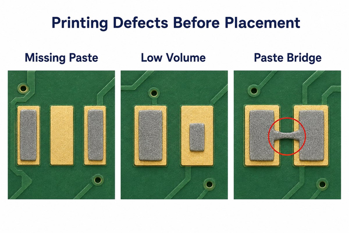
- Missing or low-volume paste: investigate blocked apertures, release behavior, paste condition, and print settings.
- Excess paste: check aperture design, stencil contact, support, and the printing setup.
- Deposit offset: review alignment, fiducial recognition, board movement, and registration.
- Paste bridging or smearing: examine stencil underside contamination, separation behavior, support, and material handling.
The pattern helps narrow the investigation. A problem confined to one aperture differs from a whole-board shift or a gradual trend across many prints. SPI identifies what changed; confirming the cause still requires examining the printing process.
Do not label a print as a “cold solder joint.” That term describes a soldering outcome, whereas SPI takes place before solder has reflowed. The later thermal and metallurgical conditions have not yet occurred.
What Should Happen After an SPI Failure?
Hold the affected board before component placement and verify the call. Review the image or height map, the failed value, the target, and the program revision before making a disposition.
If the print is genuinely unacceptable, follow the approved cleaning and reprinting procedure for the board and paste system. Do not assume that adding paste by hand produces the same controlled deposit as a qualified printing process.
Then address recurrence: check the stencil, board support, print alignment, underside cleaning, paste handling, and relevant printer settings. After a correction, inspect a new print and verify that the original problem is resolved without introducing a different one.
For repeated failures around small apertures, review the SMT stencil as well as the machine settings. An inspection threshold cannot repair an aperture design that does not release paste consistently.
How Is SPI Different from AOI?
SPI evaluates the print before placement; AOI evaluates visible features at its configured inspection stage. They answer different questions and should not be treated as substitutes.
| Inspection | Typical stage | Main target |
| SPI | After paste printing | Deposit geometry and position |
| Pre-reflow AOI | After placement, where used | Visible component presence and placement |
| Post-reflow AOI | After soldering | Visible component and joint features |
Hidden solder connections may require other inspection methods, and electrical defects require appropriate testing. Neither an SPI pass nor an AOI pass proves every functional requirement. For the later optical stage, see our guide to AOI in PCB manufacturing.
How Can SPI Data Improve Printing Control?
Trend data can reveal drift that an isolated pass/fail result hides. Track comparable deposit groups by board, print sequence, stencil revision, and relevant process events rather than averaging unrelated pads into one reassuring number.
For example, a consistent directional offset may justify checking alignment, while falling volume in a particular aperture group may prompt a stencil-release investigation. Compare the trend with cleaning cycles and setup changes before assigning a cause.
Some printer and SPI combinations support integrated feedback. Such a connection needs compatible equipment, validated correction rules, and limits on what the system may adjust. It should not be assumed present on every SMT line, and it should not turn an unresolved measurement problem into an automatic printer correction.
What Should an SPI Report Contain?
A useful report lets an engineer trace a result to the board, deposit, program, and disposition. A green dashboard without that context is difficult to investigate later.
- Board or panel identifier, inspection time, and product revision.
- SPI program revision and the applicable pad or deposit group.
- Measured values, units, nominal references, and acceptance limits.
- Images or height maps for reviewed exceptions.
- Release, hold, reprint, or other approved disposition.
- Relevant process changes and links to downstream inspection or test records.
Specify the required records before production if they are part of your quality agreement. Retention, serialization, and reporting formats should be agreed for the project rather than assumed from the presence of an SPI machine. Our overview of PCB testing explains how inspection fits into a broader verification plan.
How Can EBest Circuit Support Your PCB Assembly Inspection Plan?
At EBest Circuit, we provide PCB fabrication and PCBA assembly support, including solder paste inspection within our SMT capabilities. We can review your board data, component requirements, and inspection expectations together so the manufacturing and verification plan matches the assembly.
If your starting question is what is solder paste inspection, the next step is to identify which print characteristics matter for your components and which records your project needs.
Send your Gerber files, BOM, placement data, quantity, and inspection or traceability requirements to sales@bestpcbs.com. We will review the assembly scope with you, including any package-specific checks that need to be agreed before production.