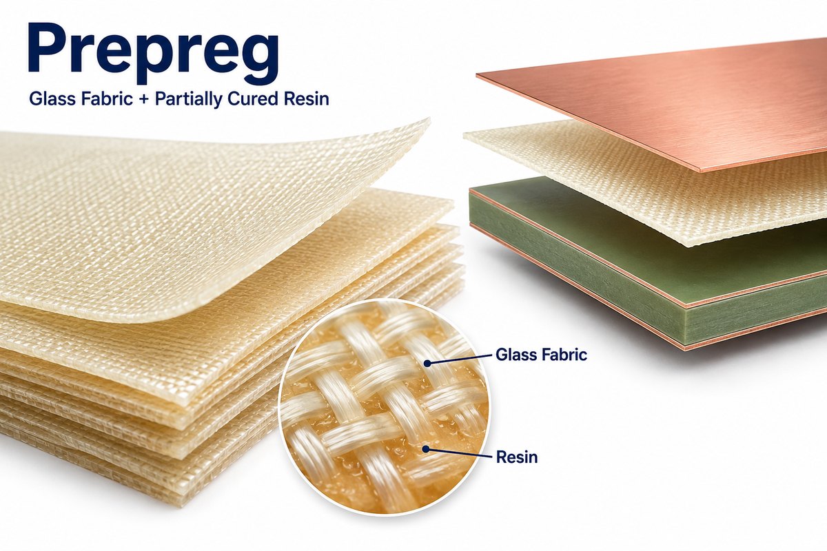
Prepreg is a reinforcement material already impregnated with resin. In conventional multilayer PCBs, it usually means woven glass fabric containing partially cured thermosetting resin. During lamination, that resin flows around copper features and then cures, bonding the stack while electrically separating adjacent conductor layers.
Choosing prepreg affects dielectric spacing, impedance, resin filling, and manufacturability. The glass style alone is not a complete material specification: the resin system, resin content, ply count, and pressed construction also matter.
What Is PCB Prepreg Made Of?
PCB prepreg combines a reinforcing fabric with a controlled resin formulation. The fabric provides a supporting structure, while the resin supplies bonding and contributes to the finished dielectric’s electrical and thermal behavior.
For many FR-4 constructions, the reinforcement is electrical-grade woven glass and the resin is epoxy-based. Other material families use different formulations for requirements such as lower loss, higher thermal performance, or controlled flow.
The supplier impregnates the fabric and advances the resin to an intermediate state, commonly called B-stage. Conventional PCB prepreg is handled as a sheet, but it remains reactive. After the qualified lamination cycle, the resin becomes a cured part of the board.
“Prepreg” describes the material form, not a single performance grade. It is also used outside electronics, including carbon-fiber composites. Those materials should not be treated as interchangeable with the insulating glass-reinforced bonding sheets specified for a PCB.
PCB Prepreg vs Core
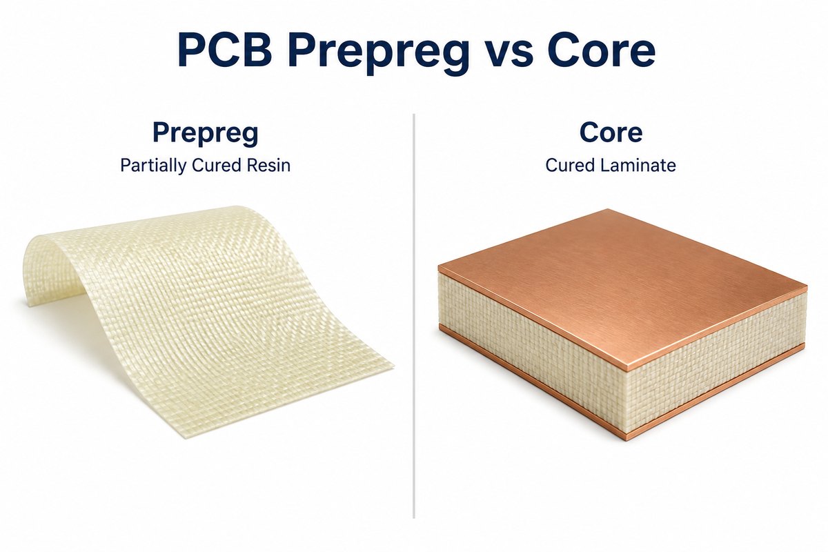
The main distinction in PCB prepreg vs core is the cure state before multilayer lamination. A core is already a cured laminate; prepreg supplies resin that can flow and bond during the next pressing operation.
| Feature | Prepreg | Core |
| Resin state before layup | Partially cured | Already cured |
| Typical supplied form | Resin-impregnated reinforcing sheet | Rigid laminate, often copper-clad |
| Role during pressing | Bonds layers and fills copper topography | Provides an existing dielectric layer and circuit support |
| Thickness for stackup design | Use the fabricator’s pressed construction | Use the specified laminate thickness and tolerance |
In a common four-layer foil construction, the two inner copper layers are patterned on a double-sided core. Prepreg and outer copper foil are placed on each side and laminated into one board. The prepreg-derived layers are solid dielectrics in the finished PCB; they do not remain loose adhesive sheets.
A core and a prepreg construction with similar nominal thickness are not automatically interchangeable. Their electrical properties, tolerances, and manufacturing roles may differ. For the broader layer arrangement, see our PCB board stackup guide.
PCB Prepreg Types
PCB prepreg types can be described by glass style, resin family, resin content, and flow behavior. These describe different attributes, so a designation such as “1080” should not be mistaken for a complete product grade.
- Glass style: familiar examples include 106, 1080, 2113, 2116, and 7628. The numbers identify fabric constructions, not universal finished thicknesses.
- Resin family: options include conventional epoxy-based systems and specialized formulations for thermal or high-frequency requirements.
- Resin content: a product may offer several resin percentages using the same fabric.
- Flow behavior: standard-flow and controlled- or low-flow products serve different bonding needs.
- Weave construction: spread-glass options can be relevant where local dielectric variation matters.
Terms such as standard, medium, or high resin are supplier-dependent descriptions. Specify the actual product and resin percentage when the design depends on them. Similarly, “high Tg” does not define dielectric loss, moisture behavior, or every aspect of thermal reliability.
For thin HDI dielectrics, glass construction must also suit the intended microvia process. A material appropriate for a conventional multilayer board is not automatically suitable for every laser-drilled build-up.
Prepreg PCB Thickness
Prepreg PCB thickness should be evaluated as a pressed dielectric construction, not simply the thickness of a loose sheet. During lamination, resin redistributes into the spaces around etched copper and the stack consolidates.
Keep three measurements separate: dry glass fabric thickness, supplied prepreg sheet thickness, and cured dielectric thickness in the board. A value taken from one category should not be entered into a calculator as another.
The following examples come from Isola’s published IS420 prepreg construction table. They show why a glass style needs its resin content alongside it. These are product-specific listed values, not guaranteed pressed thicknesses for every PCB design.
| IS420 glass style | Resin content | Listed thickness |
| 1080 | 64% | 0.073 mm |
| 1080 | 70% | 0.090 mm |
| 2116 | 52% | 0.116 mm |
| 2116 | 57% | 0.132 mm |
The fabricator must translate material data into a buildable stackup using the actual copper pattern, press process, and ply arrangement. Ask for the target dielectric spacing and its tolerance at the relevant layer pair, not just a nominal overall board thickness.
Also clarify whether a core dimension includes its copper cladding. Mixing copper-inclusive and dielectric-only dimensions can make a thickness calculation look correct while counting copper twice. A finished-board thickness requirement and an impedance-critical dielectric spacing are separate controls.
How Does Resin Content Affect Copper Filling?
Resin must fill the spaces around the copper pattern while leaving the required dielectric separation. Copper thickness and the amount of copper retained on each layer therefore influence the bonding construction.
A sparse circuit pattern leaves more space to fill than a nearly solid plane of the same copper thickness. Heavy copper creates taller features. Both conditions can increase the importance of resin volume and flow control.
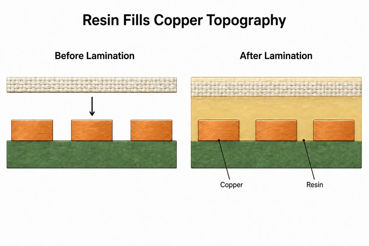
Resin content and resin flow are not the same property. Content describes how much resin the material contains; flow depends on the formulation, cure advancement, temperature history, pressure, and construction. A higher resin percentage does not by itself guarantee successful filling.
Selection should balance fill requirements with the final thickness and electrical targets. If a fabrication review calls for a different resin content or additional ply, reassess the affected dielectric spacing rather than treating the change as a purchasing detail.
PCB Prepreg Dielectric Constant
PCB prepreg dielectric constant, usually written Dk, is a property of the resulting resin-and-reinforcement construction under specified test conditions. It is not one fixed number for all FR-4 prepregs.
Glass type, resin formulation, resin proportion, frequency, and test method influence the value used in design. Df describes dielectric loss and must be considered separately. A material can meet a thickness target without meeting the loss budget for a fast channel.
For controlled impedance, use construction-specific data agreed with the fabricator. Specify the reference layer, trace geometry, copper thickness, and required impedance tolerance. A generic library value may be useful for an early estimate but should not silently become the released manufacturing assumption.
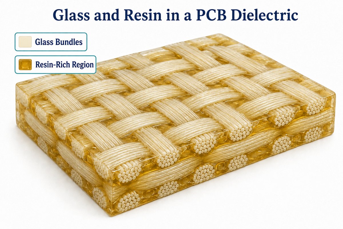
The weave also creates local differences between glass-rich and resin-rich regions. For sensitive high-speed channels, routing orientation and available spread-glass constructions may deserve review. The appropriate response depends on the channel requirements; not every board needs a specialized weave.
Our high-speed PCB design guide explains how material decisions interact with routing and signal integrity.
What Happens to Prepreg During Lamination?
During a qualified lamination cycle, the resin softens and flows, wets the prepared interfaces, and progresses toward full cure. The process must provide enough time for filling before the resin loses its ability to flow.
- Prepare and verify the inner layers and bonding surfaces.
- Lay up the specified cores, prepreg plies, and copper foil in the correct sequence.
- Apply the validated thermal, pressure, and vacuum conditions where required.
- Complete the required cure and controlled cooling.
- Verify the resulting construction and applicable acceptance requirements.
There is no single press temperature or pressure recipe for all prepregs. Supplier guidance is a starting point that must be matched to the fabricator’s equipment and board construction. Hybrid materials and sequential lamination need their own compatibility and thermal-history review.
PCB Prepreg Shelf Life
PCB prepreg shelf life depends on the specific product, storage conditions, and exposure history. Use the current supplier instructions and lot documentation instead of a blanket rule such as “all prepreg lasts six months.”
Temperature, humidity, and moisture-barrier packaging matter. Material taken from colder storage should remain sealed while it equilibrates to the layup environment when the supplier requires this, helping avoid condensation on the sheets.
- Track material grade, lot, receipt date, expiry basis, and opened-package exposure.
- Use clean gloves and protect sheets from contamination and fabric damage.
- Reseal unused material according to the product instructions.
- Keep expired or improperly stored material on hold until an approved disposition is available.
Do not assume that baking restores an aged prepreg to its original condition. Moisture removal and resin cure advancement are different issues, and an improvised treatment may change the flow needed during pressing.
Which Problems Can an Unsuitable Prepreg Construction Cause?
An unsuitable construction or poorly controlled process can contribute to resin starvation, voiding, inadequate bonding, or incorrect dielectric spacing. These symptoms need investigation; they do not identify prepreg as the sole cause.
For example, a bonding defect can involve contamination, moisture, inner-layer preparation, cure conditions, or a material mismatch. Review the material lot and handling history together with the lamination records and physical evidence.
For thickness or impedance deviations, compare the released stackup with the actual material construction and measured board. Checking only the material family name can miss a change in glass style, resin content, or ply count.
Cross-sections and other agreed inspections can help verify layer geometry and investigate interfaces. Where separation is suspected, our PCB delamination guide discusses the broader manufacturing and handling factors.
What Should the Fabrication Notes Specify?
Specify the performance and construction details needed to protect the design, while leaving room for a reviewed manufacturing solution where appropriate.
- Approved laminate and bonding-material family, with substitution rules.
- Layer sequence, finished thickness, and critical dielectric spacings.
- Copper thicknesses and controlled-impedance requirements.
- Glass style, resin content, or ply count where these are design-critical.
- Thermal, loss, insulation, and reliability requirements relevant to the product.
- Required stackup approval and inspection records.
If you specify only a brand and “FR-4,” the fabricator still needs to resolve the construction. If you prescribe every ply without checking availability, the result may be unnecessarily difficult to source. Agree the stackup before routing dimensions are frozen, especially for high-speed or unusual copper structures.
Availability also affects cost and delivery. A standard construction already qualified by the fabricator may avoid a special material order, while an uncommon glass-and-resin combination can require additional procurement or validation. Ask which requirements are fixed and which equivalent constructions can be reviewed. Savings should come from an agreed alternative, not an undocumented substitution after the layout has been approved.
Material substitutions should be reviewed for more than nominal Tg. A change can alter pressed spacing, Dk, Df, flow, or processing compatibility. Our guide to glass transition temperature in PCB materials explains why Tg is only one part of that assessment.
How Can EBest Circuit Support Your PCB Stackup?
At EBest Circuit, we provide PCB fabrication and PCBA services, including multilayer and impedance-controlled boards. We can review your proposed stackup alongside the copper layout, material requirements, and assembly needs before the design moves into production.
If you need help selecting a prepreg construction, send your Gerber files, proposed layer stack, copper thicknesses, impedance targets, and order quantity to sales@bestpcbs.com. Include any approved material list or substitution restrictions so we can discuss suitable manufacturing options for your project.