DFX design brings manufacturing, assembly and test requirements into PCB development before the layout is released. DFX means design for X, with X representing a design objective; design for excellence is another common name. For a PCB, the immediate questions are whether the bare board can be fabricated, the components can be assembled, and the finished assembly can be tested.
A layout can pass electrical design-rule checks yet contain an impractical BGA escape pattern, leave too little space for rework, or hide a test point behind a fitted connector. PCB DFX addresses those problems while the designer can still change placement, routing or the planned process. Reliability requirements add another question: will the assembly withstand its intended operating conditions?

How Does DFX Differ from DFM, DFA and DFT?
DFX is the umbrella approach. DFM, DFA and DFT address different production tasks within it:
- DFM — design for manufacturing or manufacturability: checks bare-board construction against the fabricator’s process. A trace, hole or stackup must meet both the design requirement and the selected manufacturing capability.
- DFA — design for assembly: checks how parts will be placed, soldered, inspected and reworked. A footprint that fits electrically can still create an assembly-access problem.
- DFT — design for test or testability: provides the access and circuit conditions needed to detect specified faults or verify functions. A reachable pad is useful only when the planned test can obtain a meaningful result through it.
DFMA combines manufacturing and assembly considerations. Some suppliers also use DFM as shorthand for both, so confirm what their review includes. A broader DFX review brings the affected teams together; a fabrication approval alone does not establish assembly test coverage or product reliability.
Why Should DFX Principles Be Applied Before PCB Production?
Early review exposes conflicts before routing, tooling and procurement make them harder to resolve. Moving a connector during placement may be straightforward. Moving it after a fixture and enclosure have been built can require changes to all three.
Useful DFX principles turn those consequences into design decisions:
- Design to an agreed process. Obtain the intended fabricator’s stackup and geometry constraints. A prototype made through a different process does not prove that the production route is suitable.
- Reserve assembly and test access before placement is fixed. Ask the assembly and test teams what space their equipment needs. Add the resulting keepouts to the layout while alternatives remain practical.
- Preserve electrical and reliability requirements. Widening a trace, moving a component or adding a test pad can affect impedance, return paths or thermal behavior. Recheck the affected requirement before accepting the change.
- Verify repeatability. Hand-assembling one prototype may conceal access or handling problems in the intended production sequence. Use build feedback to check whether the proposed process works consistently.
What Does DFM Check in a PCB Design?
In a PCB DFX manufacturing review, DFM checks whether the selected process can produce the specified board. Use the actual stackup, copper requirements and hole structure, rather than a generic minimum-feature table.
- Traces, spaces and copper clearance. Check narrow routes, BGA escape areas and copper near the board edge against the agreed fabrication rules. If a change is required, verify its electrical effect as well as its manufacturability.
- Holes, annular rings and vias. Confirm drill sizes, finished-hole requirements, layer spans and the proposed via process. A smaller hole or an added microvia may require a different fabrication route; it is not automatically a safe way to free routing space.
- Stackup and controlled impedance. Agree on the layer construction and impedance requirements before final routing. A nominal line width without the corresponding dielectric and copper geometry is not a complete controlled-impedance instruction.
- Mask, outline and panel features. Review solder-mask openings, edge clearances, slots, cutouts and any panel requirements. Resolve differences between the drawing and exported geometry before the fabricator prepares production data.
Record the agreed process and any exceptions in the fabrication package. Detailed PCB design for manufacturing work should leave the fabricator with requirements it can evaluate, rather than instructions to make unspecified changes during CAM preparation.
What Does DFA Check Before PCB Assembly?
DFA checks the populated board and the operations needed to build it. Review the actual package variants and component bodies, not only the copper pads.
- Footprints, polarity and orientation. Match the footprint to the ordered part’s package drawing. Check pin numbering, polarity marks and rotation conventions against the BOM and placement data; a matching designator does not prove the correct package was used.
- Land pattern and solder-paste design. Check the footprint, solder-mask openings and stencil apertures as one assembly decision. For QFN/SON packages, use the device recommendations and TI’s QFN/SON assembly guidance to evaluate pad geometry and solder-paste deposition, then confirm the details with the assembler.
- Placement, soldering and rework access. Check tall parts, connectors and neighboring packages against the equipment approach. A component may be placeable but difficult to remove without heating or disturbing its neighbors.
- Inspection and handling. Identify which joints are visible to the planned optical inspection and which need another method. Agree on board support and panel handling where those operations could interfere with fitted components.
A courtyard check is a useful starting point, but it only tests the clearance represented in its rules. The assembly team still needs to confirm the intended process and access.
What Does DFT Check for PCB Testing?
DFT starts with what the test must detect, then works backward to the required access and circuit state. Separate bare-board continuity/isolation testing from testing a populated PCB assembly; they address different defects.
- Test method and coverage. Identify the faults or requirements addressed by in-circuit testing, flying probes, functional testing or another selected method. State the gaps instead of treating one test name as complete coverage.
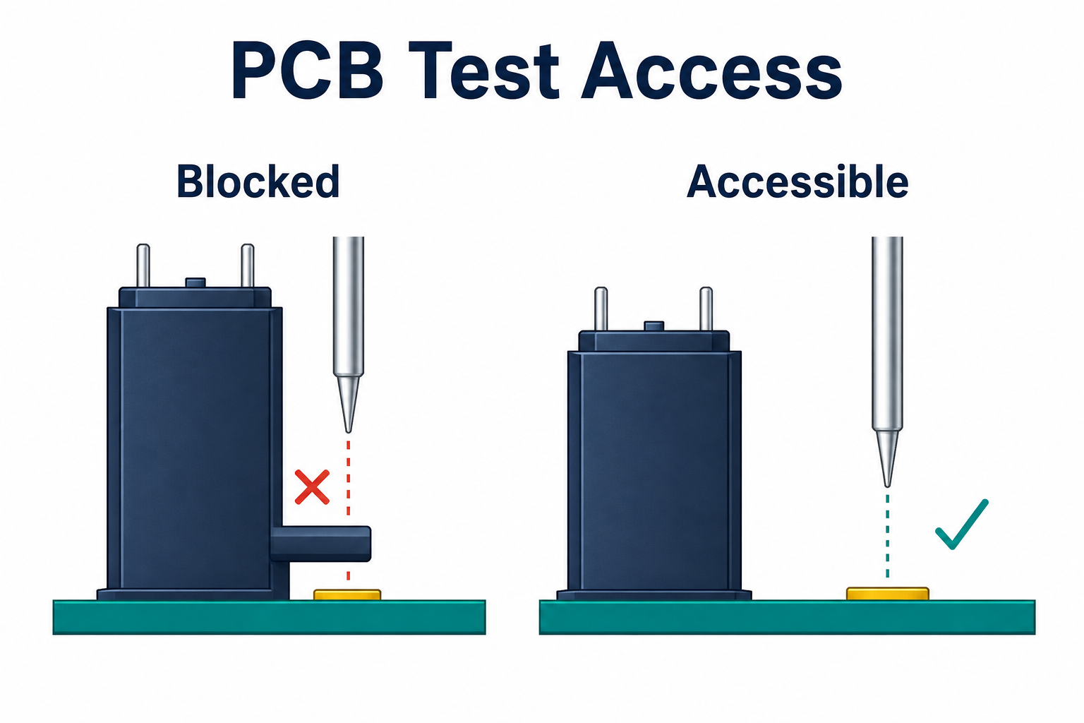
- Physical access. Check probe approach, contact area and surrounding component height in the intended test configuration. Agree on dimensions with the test team; a pad that is visible in a bare-board view may be blocked after assembly.
- Electrical access and board state. Define power, ground, reset, programming and measurement conditions. Boundary scan or self-test can help where supported and implemented, but neither is available merely because the board has a connector.
- Measurement limits and signal integrity. Set pass/fail limits appropriate to the circuit and test setup. Review added pads, branches and loading on sensitive nets before releasing test-access changes.
The result should connect each required test to an interface, operating condition, measurement and acceptance limit. Keep inaccessible or untested requirements visible in the test plan.
How Does DFR Support PCB Reliability?
Design for reliability checks whether the assembly can withstand its expected loads and environment. Define temperature, duty cycle, humidity, vibration and service-life requirements where relevant, then investigate the failure mechanisms they can drive.
For a power device, review the heat path through its package and PCB, then verify temperatures under representative load and enclosure conditions. For a board carrying connector loads, review mounting and mechanical support. Environmental protection must also remain compatible with assembly, test and any required repair.
Passing a production functional test does not prove service life. DFR may require thermal analysis, stress assessment or environmental validation beyond the DFM, DFA and DFT checks.
When Should You Perform a PCB DFX Review?
Begin before architecture and placement decisions are fixed, and repeat the relevant checks as the design matures.
- Before detailed layout: agree on the fabrication route, likely assembly process and test strategy. The output is a usable set of constraints for stackup and placement.
- During placement and routing: review dense packages, access regions and mechanical interfaces. Resolve conflicts while components and routes can still move.
- Before fabrication release: review matching design files and close build blockers. Record any accepted exceptions against the released revision.
- After prototype or pilot builds: examine actual assembly problems, test failures and validation results. Update the design or process and verify the affected requirements before the next build.
A manufacturer change, package substitution or test-method change should trigger a focused reassessment even if the schematic has not changed.
What Do Practical PCB DFX Examples Look Like?
The following are illustrative engineering scenarios, not measured factory case studies. Each shows how a finding becomes a design decision and what evidence would close it.
Example 1 — DFM: a BGA escape pattern exceeds the chosen process
Situation and risk: Routes between BGA pads require trace/space geometry or vias outside the fabricator’s agreed process. A clean electrical DRC can miss this mismatch if its rules do not represent that process.
Proposed change: Review the exact package guidance, escape routing and stackup with the fabricator. Consider rerouting, another layer arrangement or a supported via structure. If the package requires a different fabrication route, establish that before committing the layout.
Verification: Obtain confirmation for the revised geometry, rerun manufacturing checks and recheck affected electrical constraints. For an unproven package/process combination, review prototype evidence before volume production; supplier acceptance of a drawing is not a measured yield result.
Example 2 — DFA: a tall connector blocks QFN rework access
Situation and risk: A connector fits beside a QFN in the placement view but obstructs the planned rework nozzle. Removing the QFN could disturb nearby parts or expose them to excessive heat.
Proposed change: Move the connector or reserve the access region required by the assembler’s rework method. Check the enclosure fit and affected routing before accepting the new position.
Verification: Review the populated-board model with the actual tool dimensions, then validate the proposed rework operation on representative hardware where required. Closure needs evidence of usable access and acceptable results, not just a larger CAD courtyard.
Example 3 — DFT: a test point disappears behind a fitted component
Situation and risk: A test pad is exposed on the bare PCB but lies beneath a connector overhang after assembly. The fixture cannot contact it at the intended test stage, leaving a required measurement unavailable.
Proposed change: Relocate the pad to an accessible area, provide another suitable interface, or revise the test sequence. If testing moves earlier, identify which later assembly faults that test will no longer detect.
Verification: Recheck connectivity and signal loading, prove contact access on the populated board, and demonstrate the required measurement with repeatable contact. Update the coverage record before closing the finding.
How Do You Perform a PCB DFX Analysis?
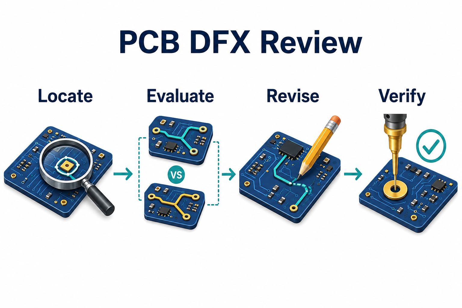
A DFX analysis links a specific design feature to a production risk, a decision and verification evidence. The PCB designer owns design changes, while fabrication, assembly, test and product specialists supply the constraints and evidence for their areas.
- Establish the review basis. Identify the board revision, assembly variant, supplier process and applicable acceptance criteria. Resolve missing or conflicting inputs before making findings that depend on them.
- Record actionable findings. Give the location, affected operation and evidence. For example, identify the obstructed pad and fixture approach, rather than writing “improve testability.” Separate confirmed violations from questions needing investigation.
- Agree on a disposition. Assign an owner and proposed correction. Consider its effect on the other DFX objectives and distinguish build blockers from improvements that can wait for a later revision.
- Verify and close. Check the corrected revision using the appropriate design review, measurement or build evidence. Retain the result with the finding; a risk accepted without correction needs an identified approver and reason.
What Files Are Needed for a PCB DFX Review?
Provide matching fabrication, assembly and test information for one identified revision. The review scope determines the necessary inputs:
- Fabrication: supply Gerber and drill data, or an accepted ODB++ package, with the fabrication drawing, stackup and controlled-impedance requirements. The fabricator needs both geometry and build instructions.
- Assembly: supply the BOM with exact part numbers and fitted variants, assembly drawings and pick-and-place data identifying positions, rotations and board sides. Check that designators and fitted parts agree across these files.
- Testing: supply schematics, relevant net information, programming requirements and the test specification. State the intended board configuration and acceptance limits so the test team can assess access and coverage.
- Mechanical and reliability review: supply component/enclosure geometry and relevant operating conditions. The responsible engineers need those constraints to judge clearance, support and thermal requirements.
If the BOM and layout disagree, identify the intended variant and reissue a consistent package. Do not assume that the newest individual files belong to the same release.
What Should a PCB DFX Checklist Confirm Before Release?
A release checklist confirms that the review has produced usable decisions and evidence. Use the following items to decide whether the design can proceed through the agreed process; they do not replace the detailed checks above.
| Design Item | Release Check and Purpose |
|---|---|
| Board geometry | Confirm that the fabricator accepts the released trace, hole and via requirements. This resolves the process mismatch identified during DFM. |
| Stackup | Confirm the agreed construction and impedance requirements. Review electrical effects if manufacturing changes altered the geometry. |
| Assembly access | Confirm the fitted packages and intended placement, soldering and rework access. Resolve obstructions before committing assembly tooling. |
| Test coverage | Match required checks to usable access, board states and acceptance limits. Record gaps so physical access is not mistaken for fault coverage. |
| Reliability risks | Confirm that required analysis or validation is complete for this release stage. Carry any permitted open work forward with an owner and acceptance basis. |
| Release identity | Match files and closed findings to the same revision and variant. Obtain approval for remaining exceptions before ordering the build. |
Download the editable DFX review template (CSV). Use one row per finding to record its location, consequence, owner, action and closure evidence.
FAQs About DFX Design
Q1: Is DFX the same as FMEA?
A1: No. Failure mode and effects analysis (FMEA) examines potential failures, their causes and effects to guide risk treatment. DFX is the broader approach to designing for manufacturing, assembly, testing and other selected objectives. FMEA can help prioritize a DFX change, but a manufacturing or access review is not automatically an FMEA.
Q2: Is a DFX review worthwhile for a small prototype batch?
A2: Yes, with a scope matched to the build. A dedicated production fixture may be unnecessary, but an unbuildable footprint or inaccessible programming interface can still stop a prototype. Check immediate blockers and record which volume-production assumptions remain unverified.
Q3: Does 100% test-point access mean 100% fault coverage?
A3: No. Access describes what can be contacted; coverage describes what the tests can detect. A reachable net may not reveal a particular component fault. Define the fault set or requirements behind the coverage figure and document the tests and remaining gaps.
Q4: Does an approved DFX report transfer to a new manufacturer?
A4: It provides useful history, but the new process needs its own assessment. Stackups, tolerances, assembly equipment and fixtures may differ. Retain applicable findings and rerun checks whose assumptions changed, binding the new approval to the supplier and revision.
Q5: Can DFX software replace engineering review?
A5: Software can screen supported features against configured rules, but engineers must verify the inputs and interpret the results. Check library data, supplier constraints, waived findings and requirements the tool does not model. An empty error list does not establish complete manufacturability, test coverage or reliability.
How Do You Turn DFX Findings into a Better PCB?
Use DFX design to resolve specific production problems before release: an unsupported escape pattern, an obstructed rework area or an unavailable test connection. Agree on the change with the affected teams, then verify it against the correct revision. The value comes from resolving those problems without creating new electrical, assembly or reliability risks.
Send your PCB design files and BOM to EBest Circuit at sales@bestpcbs.com for a free DFM review. Include quantity and known fabrication, assembly or test concerns. Testability analysis and reliability validation may require additional information and a separately agreed scope.