





SiC packages do more than protect a silicon-carbide die. The selected package establishes the electrical terminals, internal interconnects, thermal path, mounting method, insulation features, and physical interface to the PCB or bus structure. Those details directly affect switching overshoot, EMI, heat removal, board area, assembly, and inspection.
This guide focuses on power-semiconductor packaging for SiC MOSFETs, Schottky diodes, and power modules. It explains how to compare common package families and translate the device choice into PCB, PCBA, cooling, and mechanical requirements.
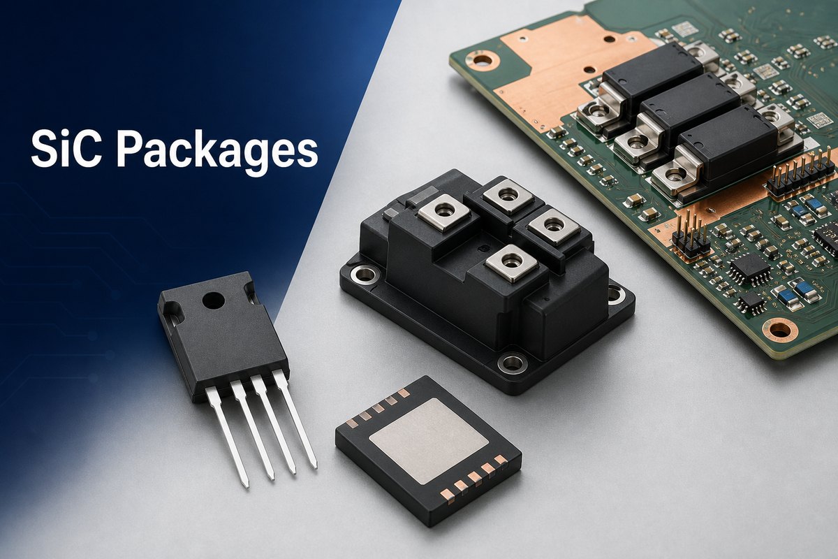
What Are SiC Packages?
A SiC package is the mechanical, electrical, and thermal structure that connects a silicon-carbide power die to the rest of the system. It may contain one device, several parallel dies, a half bridge, a three-phase bridge, temperature sensing, or other integrated functions.
The package is not the same as the semiconductor technology. Two SiC MOSFETs with similar voltage and on-resistance ratings can behave differently in the same converter because their lead arrangement, Kelvin connection, internal inductance, exposed thermal surface, insulation, and recommended layout are different.
Before creating a footprint, use the full manufacturer part number and its current datasheet. A family name such as TO-247, TOLL, or a module platform does not guarantee identical pinout, dimensions, creepage features, pad layout, mounting method, or thermal limits across suppliers.
Why Does SiC Package Choice Matter?
Package choice matters because SiC devices can switch with fast voltage and current edges. The package and PCB together form parasitic inductances and capacitances that may limit usable switching speed or create overshoot, ringing, false turn-on, common-mode current, and measurement error.
- Electrical path: lead length, terminal geometry, internal bonds, and bus overlap affect loop inductance.
- Gate control: a dedicated Kelvin-source terminal can separate the driver return from load current.
- Thermal path: heat may leave through a rear tab, a bottom pad, an insulated baseplate, or a top-side cooling surface.
- Assembly: the package may require through-hole soldering, reflow, press-fit connections, screw terminals, or controlled mounting pressure.
- Insulation: terminal spacing, exposed metal, isolation material, slots, coating, and the surrounding mechanics all influence the final insulation design.
- Service strategy: a module can simplify replacement at system level, while a dense SMD solution may reduce size but require more specialized rework.
Which SiC Package Types Are Used in Power Electronics?
Current SiC portfolios span through-hole discretes, surface-mount discretes, top-side-cooled packages, and multi-die power modules. Availability depends on device generation, voltage, current, qualification, and manufacturer, so the list below is a design map rather than a universal catalog.
| Package family | Board interface | Main design consequence |
| TO-247-3 | Through-hole, three main leads, rear thermal tab | Familiar mounting, but the shared source path can add gate-loop feedback |
| TO-247-4 | Through-hole with a dedicated Kelvin-source lead | Separates driver return from power-source current when routed correctly |
| TO-263 / D2PAK variants | Surface mount with a large bottom-side pad | Compact assembly; solder joint, copper spreading, and board thermal path are critical |
| TOLL / Thin-TOLL | Low-profile leadless surface mount | Short electrical paths and small area, with tight land-pattern and reflow control |
| TOLT / other top-side-cooled SMD | Surface mount plus a top thermal interface | Moves most heat toward a top heat sink and reduces dependence on PCB heat flow |
| Insulated power module | Pins, press-fit contacts, or terminals plus a baseplate/top cooling surface | Integrates multiple dies but adds bus, mounting, flatness, torque, and interface requirements |
TO package labels describe a mechanical family, not the complete electrical behavior. Compare the exact package drawing, pin assignment, isolation construction, thermal impedance, stray inductance data, land pattern, and mounting note for the selected orderable part.
SiC MOSFET Packages
SiC MOSFET packages are often compared by voltage and current rating first, but the board should be planned around four additional questions: where the switching current flows, where the gate current returns, where the heat exits, and how the part is assembled.
A three-lead through-hole package can be practical for established mechanical designs and lower-density production. A four-lead version provides a Kelvin-source connection, but only delivers its intended benefit when the gate driver returns to that dedicated terminal instead of sharing the high-current source route. Surface-mount packages shorten connections and support automated placement, yet exposed-pad soldering and heat spreading become part of the PCB design.
Do not copy a silicon MOSFET footprint or gate network solely because the outline looks familiar. Faster SiC switching can expose inductance, coupling, probe-access, and insulation weaknesses that were acceptable in the earlier design.
How Do SiC Power Modules Differ from Discrete Packages?
SiC power modules place multiple power dies and internal interconnects in one package, often on an insulated ceramic-metal substrate. A module can reduce the number of separate power packages and offer a compact bridge structure, but it does not remove the need for low-inductance external connections, controlled cooling, and coordinated mechanical design.
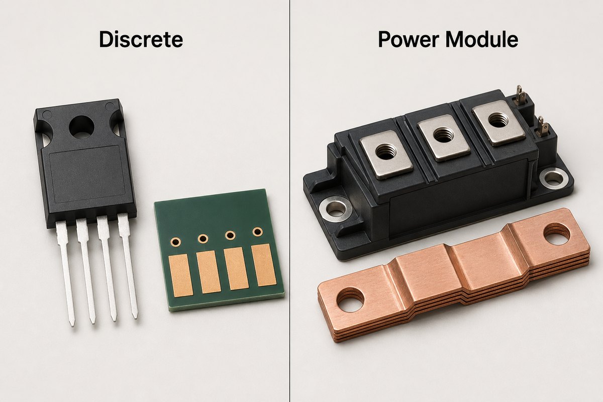
| Decision area | Discrete packages | Power modules |
| Power-stage flexibility | Individual devices can be arranged for the required topology | Topology and internal connections are partly fixed by the module |
| External interconnect | PCB copper commonly carries power and gate connections | PCB, busbar, terminals, or press-fit structures may share the interconnect task |
| Cooling | Managed per device through tab, bottom pad, or top surface | Managed through a larger insulated baseplate or top cooling interface |
| Assembly | THT or reflow processes; more individual placements | Fewer power placements, but tighter mounting, flatness, and torque control |
| Repair approach | A single device may be replaceable, depending on layout and damage | The module is normally treated as one replaceable unit |
For a new sic power module design, freeze the electrical topology and the cooling/mechanical stack together. Selecting a module after the PCB outline is fixed often creates long bus paths, obstructed driver placement, or an impractical heat-sink interface.
What Does SiC Power Module Packaging Need from the PCB?
SiC power module packaging needs a PCB and mechanical assembly that respect the module’s terminal map, isolation boundary, cooling surface, and mounting sequence. The control PCB may carry gate-drive and sensing connections while a busbar or separate copper structure carries the main current.
- Keep gate-driver connections short and matched where parallel switches or bridge legs require symmetry.
- Place local DC-link capacitors so their current loop to the module terminals is physically compact.
- Do not route sensitive sensing lines beside high-dv/dt nodes or through the high-current return path.
- Include tolerance for terminal position, press-fit holes, connector engagement, mounting holes, and heat-sink flatness.
- Define torque, mounting order, thermal-interface material, and allowable mechanical stress from the module supplier’s instructions.
- Provide safe probe access for gate voltage, switch-node behavior, current measurement, and temperature validation.
Some modules expose an electrically insulated cooling surface; others require additional insulation. Never infer isolation from appearance. Use the exact module documentation and the end-product safety standard.
How Does a Kelvin Source Change the PCB Layout?
A Kelvin-source pin gives the gate driver a dedicated reference closer to the semiconductor source potential. It reduces the unwanted voltage in the gate loop caused by load-current di/dt through a shared source inductance.
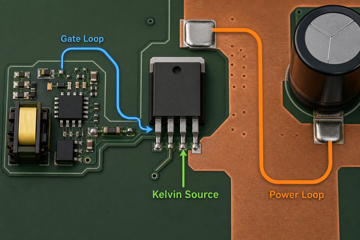
The PCB must preserve that separation:
- Return the driver’s source/reference connection directly to the Kelvin-source terminal.
- Carry load current through the main source terminal and its wider power path.
- Place the driver, local isolated supply decoupling, and gate resistor close to the MOSFET.
- Avoid overlapping the gate path with drain or switch-node copper where capacitive coupling can inject noise.
- When devices are paralleled, review gate-path symmetry and the manufacturer’s recommended gate-resistor arrangement.
A Kelvin terminal is not a license to lengthen the gate loop. Package inductance, via transitions, connector inductance, and the external return geometry still affect switching behavior.
How Should the Commutation and Gate Loops Be Routed?
Route the commutation loop and gate loop as two deliberately controlled structures. The high-current loop should be short and use closely coupled outgoing and return conductors. The gate loop should be compact, protected from the switch node, and referenced to the correct source terminal.
- Place the local DC-link capacitor first. Put it across the switching cell before routing peripheral power paths.
- Minimize loop area. Use overlapping planes or closely spaced conductors where voltage and insulation constraints allow.
- Keep switch-node copper purposeful. It must carry current and spread heat, but excess area can increase capacitive coupling.
- Place the driver next to the device. Long control traces add inductance and make the gate more vulnerable to noise.
- Separate sensing from power current. Current shunts, desaturation protection, temperature sensing, and voltage dividers need controlled reference paths.
- Design measurement access. Probe loops and long ground leads can misrepresent fast waveforms; plan low-inductance test connections.
For systems above basic low-voltage logic levels, package spacing is only one part of the insulation path. Our high-voltage PCB design guide explains why working voltage, transients, pollution degree, altitude, material group, coating, slots, and nearby metalwork must be reviewed together.
How Do Top-Side and Bottom-Side Cooling Differ?
Top-side cooling sends heat directly from the package’s exposed upper surface to a heat sink or cold plate. Bottom-side cooling sends heat into a soldered pad and then through PCB copper, vias, an insulated metal substrate, or a lower heat spreader.
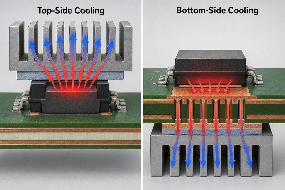
Top-side cooling can reduce the PCB’s thermal burden and free the lower board surface for routing or insulation. It introduces mechanical questions about interface compression, heat-sink flatness, package-height tolerance, electrical isolation, and assembly sequence. Bottom-side cooling can be simpler mechanically, but board thermal resistance and solder-joint quality become more influential.
For bottom-side exposed pads, thermal vias may help move heat through the board. Their diameter, pitch, plating, fill/cap method, connection to inner copper, and effect on solder wicking must be designed as one thermal and assembly system. Thermal simulation should be correlated with measurements on the assembled unit under representative load and airflow.
What PCB and Assembly Details Should Be Checked?
Manufacturing review should begin before the device footprint is locked. High-current copper, large exposed pads, mixed thermal mass, isolation slots, and heat-sink hardware can create competing fabrication and assembly requirements.
- Footprint source: use the current package drawing and recommended land pattern for the exact part number.
- Copper construction: state finished copper, plated features, current paths, copper balance, and any heavy-copper transition.
- Stencil design: divide large paste apertures where needed and define the target from package and process guidance.
- Reflow and moisture handling: follow the component’s package-specific limits; do not apply a generic profile to every SiC device.
- THT handling: control lead forming, insertion, solder fill, component standoff, heat-sink attachment, and mechanical load.
- Module mechanics: document coplanarity, hole tolerance, fastener stack, torque, thermal interface, and assembly order.
- Cleanliness and coating: confirm flux residues, coating keep-outs, coverage near high-voltage pins, and compatibility with the operating environment.
Heavy copper may support current distribution and spreading, but it also changes etching, resin fill, drilling, plating, solder mask, and reflow behavior. Review our 4-layer heavy copper PCB article when the power stage uses thick copper rather than a separate bus structure.
How Should SiC Package Assembly Be Inspected?
Inspection must match the joint and package. AOI can check visible leads, polarity, placement, and surface solder. It cannot fully assess a hidden exposed-pad joint, internal voiding, or an obscured module interface.
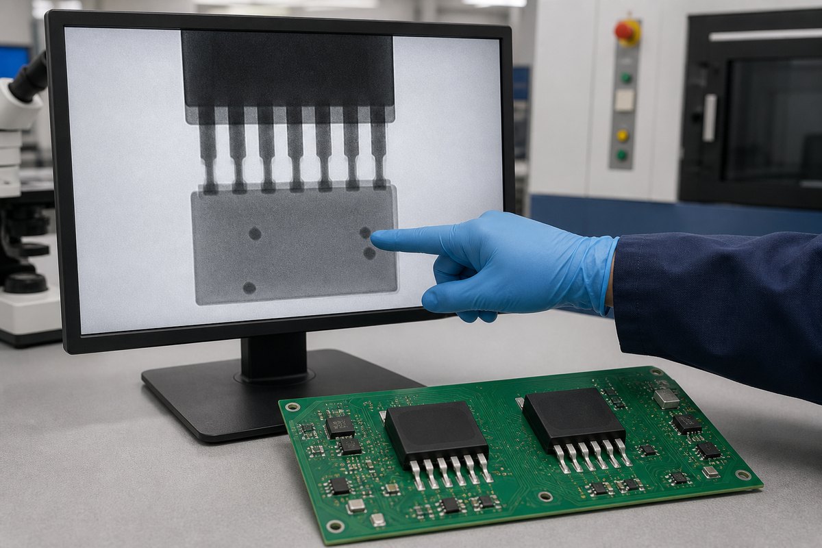
- Use AOI or visual inspection for visible terminals, alignment, solder bridges, polarity, and component damage.
- Use X-ray where the critical solder interface is hidden and the acceptance plan requires it.
- Inspect THT solder fill and lead condition according to the agreed workmanship criteria.
- Verify module seating, fastener torque records, interface coverage, connector engagement, and isolation hardware.
- Validate electrically with controlled power-up, gate-waveform checks, protection tests, temperature monitoring, and application-relevant load conditions.
X-ray inspection for PCB assembly is evidence about hidden joint geometry, not proof of complete electrical or thermal performance. Define what the image must detect and how the result will be judged before production.
Which SiC Package Fits the Application?
The best package is the one that satisfies the complete electrical, thermal, mechanical, assembly, safety, and sourcing case. A smaller outline is not automatically better, and a module is not automatically easier.
| Project priority | Package direction to evaluate | Required confirmation |
| Familiar through-hole mechanics | TO-247 family | Kelvin option, lead spacing, heat-sink isolation, and solder process |
| Compact automated assembly | D2PAK, TOLL, or related SMD family | Land pattern, stencil, void control, board thermal path, and rework |
| Direct heat extraction above the PCB | Top-side-cooled SMD package | Interface material, compression, height tolerance, and electrical isolation |
| Integrated bridge at higher power | SiC power module | Bus layout, cooling plate, terminal system, driver placement, and mounting sequence |
| Fast switching with controlled gate reference | Package with a Kelvin-source terminal | Pinout, separate return routing, gate-loop geometry, and overshoot validation |
Before release, provide the device orderable part number, datasheet revision, footprint source, schematic, Gerber or ODB++ data, stackup, copper requirements, BOM, assembly drawing, cooling stack, mechanical drawing, insulation requirements, applicable workmanship criteria, test plan, quantity, and target schedule. This package lets the PCB and assembly teams review the same physical system instead of making separate assumptions.
FAQ About SiC Packages
Are all four-lead SiC MOSFET packages Kelvin-source devices? No. Check the exact pin assignment in the datasheet. A fourth lead can support a Kelvin-source function, but package families and pin orders are not interchangeable.
Can a TO-247-4 device use a TO-247-3 PCB footprint? Do not assume so. The lead count, spacing, body dimensions, mounting geometry, and intended source routing may differ. Use the recommended footprint for the exact part.
Does a SiC power module eliminate PCB parasitic inductance? No. Internal module design can reduce some parasitics, but external bus, capacitor, gate-driver, sensing, and connector paths still contribute inductance and coupling.
Is top-side cooling always better than bottom-side cooling? No. It can shorten the heat path through the package, but it adds heat-sink, interface, tolerance, isolation, and assembly requirements. The better choice depends on the complete mechanical and thermal design.
Can solder-void limits be copied from another exposed-pad package? No. Use the device supplier’s mounting guidance, the agreed workmanship criteria, thermal model, and validated assembly process. Location and shape can matter as much as total void area.
Do faster SiC edges always improve converter performance? No. Faster switching may reduce switching loss, but can increase overshoot, ringing, EMI, common-mode current, and stress if the package and PCB loops are not controlled.
How Can EBest Circuit Support Your SiC Power PCB?
At EBest Circuit, we support PCB design review, prototyping, fabrication, component sourcing, PCB assembly, AOI, X-ray inspection, and functional-test coordination for power-electronics projects. For a SiC design, our review can connect the selected package to the footprint, stackup, copper distribution, thermal-via structure, insulation features, stencil strategy, assembly sequence, and inspection plan.
Send the exact SiC part numbers, Gerber files, BOM, stackup or current requirements, cooling and mechanical drawings, test requirements, and quantity to sales@bestpcbs.com. We will review the manufacturing package and identify PCB or assembly items that should be resolved before production. For reference during design release, keep this SiC packages guide with the approved component and mechanical documentation.







