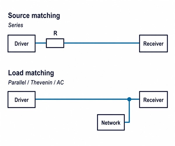
The main transmission line termination techniques in PCB design are series, parallel, Thevenin, and AC termination. Series termination matches the source; the other three place a terminating network at the load. The choice depends on where reflections occur, how much current the driver can supply, and how quickly the receiver must reach a valid logic level.
A low clock frequency does not rule out the need for termination. A fast edge can reflect along a long trace before the voltage settles, while a short trace may work without a discrete resistor. Compare the signal’s fastest edge with the route delay, then check whether the receiver stays within its voltage and timing limits under the expected operating conditions.
What Is Transmission Line Termination in PCB Design?
Termination controls reflections by changing the impedance at a transmission line’s source or load. A PCB trace and its return path have a characteristic impedance, Z0. When a traveling edge reaches a different impedance, part of the voltage wave returns along the trace. Repeated reflections can cause ringing, overshoot, or a second crossing of a clock input’s threshold.
For an ideal resistive load, the reflection coefficient is:
ΓL = (ZL − Z0) / (ZL + Z0)
A matched load gives ΓL = 0. An open circuit gives +1, producing a reflected voltage of the same polarity; a short circuit gives −1, producing the opposite polarity. These are simplified limits. Receiver capacitance, package inductance, vias, and connectors make the real response frequency-dependent.
A load terminator absorbs the wave when it reaches the receiver. A source terminator absorbs the reflection when it returns to the driver. Both can control ringing, but the voltage seen along the trace differs between them.
When Does a PCB Trace Need Termination?
Analyze termination when the route delay is significant relative to the fastest rise or fall time. Clock frequency does not describe edge speed: a 10 MHz signal can still have subnanosecond transitions. Obtain the edge rate under the intended drive strength and loading, then estimate the complete source-to-load delay.
For example, a 100 mm route with an assumed propagation delay of 6 ps/mm has a one-way delay of 0.6 ns and a round-trip delay of 1.2 ns. With a 1 ns edge, the reflection takes long enough to affect the transition. With a 10 ns edge, the same route is electrically much shorter. The assumed 6 ps/mm is not a material specification; calculate the delay from the actual stackup.
Check three things before adding a resistor:
- Interface requirements: inspect the transmitter and receiver documentation for internal termination, permitted networks, and drive settings. An external resistor may be unnecessary or harmful if matching is already on-chip.
- Route topology: identify every receiver, connector, and branch. A source-terminated point-to-point result does not establish that a multi-drop bus will settle correctly.
- Receiver margin: compare simulated threshold crossings and settling with the sampling window. For a clock, a second threshold crossing can matter even when the final voltage is correct.
How Do the Main Transmission Line Termination Techniques Compare?
The main trade-off among transmission line termination techniques is between source matching and load matching. Series termination adds little DC load at a high-impedance receiver. The load-end networks differ in their current demand, bias, and response to repeated transitions.
| Technique | Matching action | Selection condition |
|---|---|---|
| Series | Matches the source to absorb the returning wave. | One-way point-to-point route with a high-impedance receiver. |
| Parallel | Absorbs the arriving wave at the load. | Load-end matching is needed and the driver supports the DC load. |
| Thevenin | Provides load matching at a chosen bias voltage. | The interface needs both a terminating resistance and a defined bias. |
| AC | Provides load matching during a limited transient interval. | Continuous DC loading is undesirable and the signal pattern suits the RC network. |
A one-way CMOS clock with one receiver is often a good starting point for series termination. If the interface specifies a load-end network, use that circuit as the starting point instead. Differential signaling describes the interconnect mode, not a fifth passive network; its termination follows the receiver and bus specification.
How Does Series Termination Work?
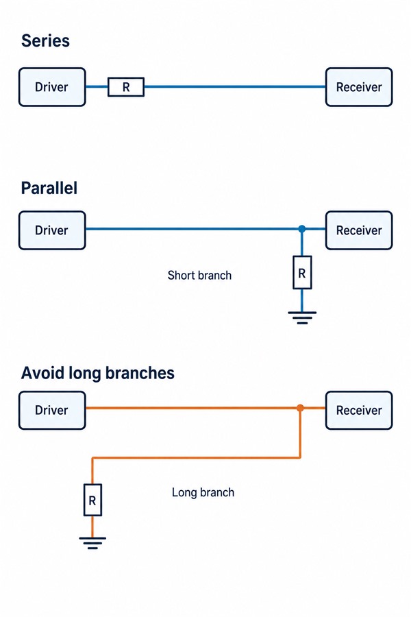
A series resistor combines with the driver’s output impedance to match Z0 at the source. Place it between the output pin and the main trace, with as little intervening copper as practical. The starting relationship is RS + Zdriver ≈ Z0.
In an ideal matched-source line with a high-impedance far end, the driver launches half of its open-circuit step voltage. At the far end, the positive reflection adds to the incident wave, so the receiver reaches the full step on the first arrival, after one one-way delay. The reflected wave then returns to the matched source and is absorbed. The receiver does not inherently have to wait for a round trip to reach the full level.
An input partway along a source-terminated trace sees the reduced step first and the returning reflection later. The intermediate voltage may sit near its switching threshold. This is why series termination works best with a single receiver at the far end, although receiver capacitance and package effects still need to be checked.
Series termination draws little steady-state current into a high-impedance load. Too much resistance can slow the edge and reduce timing margin. Check rising and falling transitions separately: the driver’s pull-up and pull-down impedances may differ. Analog Devices’ explanation of high-speed signal interfacing describes how the waves travel between the source and load.
How Does Parallel Termination Work?
Parallel termination places a resistor at the receiver or physical bus end so the incident wave sees a matched load. For a simple single-ended line, begin with RT ≈ Z0, connected to the reference required by the interface.
With a matched resistor, the arriving wave produces little reflection at the load. Keep the copper between the termination node and receiver short; any trace beyond the terminator is still unterminated. The connection to the reference also needs to be short, because its inductance weakens the match at fast edges.
The main cost is DC loading. A resistor to ground draws current in the high state; a resistor to the supply loads the low state. Calculate the actual loaded output voltage as well as resistor power. For an ideal 3.3 V source with 18 Ω output resistance driving 50 Ω to ground, the steady-state load voltage is only 3.3 × 50 / 68 ≈ 2.43 V, and the current is about 48.5 mA. Those assumed values illustrate why a correct impedance can still give an invalid logic level or excessive driver current.
Check the device’s output characteristics rather than relying on this simple resistive model. Even a smooth transition is unusable if the high level falls below VIH or the low level rises above VIL.
When Should You Use Thevenin Termination?
Use Thevenin termination when the interface needs load-end matching to a defined bias voltage. A resistor R1 connects the signal to VCC, and R2 connects it to ground. With low-impedance supply references, their parallel combination sets the terminating resistance:
Req = R1R2 / (R1 + R2)
VT = VCC × R2 / (R1 + R2)
For example, two 100 Ω resistors provide 50 Ω equivalent resistance and a 1.65 V unloaded bias from a 3.3 V supply. The undriven divider draws 16.5 mA. Driver current and resistor dissipation change when the signal is actively held high or low, so this is not the complete power budget.
Check the bias voltage as carefully as the resistance. A midpoint bias may leave the receiver at an invalid level while the line is idle or undriven. Resistor tolerance and reference noise affect both the bias and the match. Place both resistors at the load end, then check the high, low, and idle voltages against the receiver limits.
How Does AC Termination Work?
AC termination uses a series resistor-capacitor branch from the load to its reference. During a fast transition, the capacitor lets transient current flow through the resistor. After the capacitor charges, it blocks DC, reducing steady-state loading compared with a plain shunt resistor.
The match lasts only while the capacitor is charging. Too small a capacitor stops absorbing energy before the reflections settle. A larger one loads the line for longer, takes longer to recover, and draws more current during switching. The effective time constant depends on the impedances connected to the branch as well as its R and C values.
Test isolated edges, the fastest repeating pattern, and the longest allowed runs of identical bits. A network that damps an isolated edge may respond differently after several transitions. In each case, check the receiver thresholds and sampling window. TI’s comparison of differential termination techniques covers these AC-network limitations alongside resistive alternatives.
An AC termination branch connects from the load to its reference; it is not the same as a coupling capacitor inserted in the signal path. Do not substitute it for an interface-specified termination solely to reduce DC power.
How Is Termination Different for Differential Pairs?
A differential terminator matches the impedance seen between the two conductors. For a point-to-point LVDS link, a common implementation is one resistor across the receiver inputs. Its value follows the specified differential impedance and the receiver requirements.
Do not assume every differential pair needs 100 Ω. Some receivers already have a switchable internal resistor, while some buses need termination at both physical ends. Adding an external 100 Ω resistor across an enabled internal resistor of the same value gives a load of about 50 Ω, which can reduce the differential swing and overload the transmitter.
Place an external cross-pair resistor near the receiving pins with balanced connections. A resistor across the pair terminates the differential mode; it does not independently establish a common-mode bias or correct asymmetric routing. Split or biased terminations must follow the interface circuit rather than a generic substitution.
Analog Devices’ LVDS and M-LVDS implementation guide explains how point-to-point and multipoint layouts differ. Identify the physical line ends and allowed stubs before choosing the network; counting receivers alone is not enough.
How Do You Calculate Termination Resistor Values?
Start with the impedance match, then simulate nearby resistor values using the actual driver and trace. For series termination, subtract the driver’s effective output impedance:
RS ≈ Z0 − Zdriver
Worked example: assume a one-way point-to-point line, nominal Z0 = 50 Ω, estimated driver impedance = 18 Ω, and one high-impedance receiver. The starting resistor is 50 − 18 = 32 Ω. These are calculation assumptions, not measured board data.
Try 27 Ω, 30 Ω, 33 Ω, and 36 Ω in simulation. With the assumed driver, the total source resistances are 45 Ω, 48 Ω, 51 Ω, and 54 Ω. The 33 Ω resistor is closest to the nominal match; the simulations will show whether it also gives enough voltage and timing margin.
- Model the driver: use the vendor’s validated IBIS model with the intended I/O settings. Check pull-up and pull-down behavior over process, voltage, and temperature; the assumed 18 Ω will not remain constant.
- Vary the channel: include the specified impedance tolerance, receiver capacitance, resistor tolerance, packages, and vias. Compare the worst overshoot, undershoot, and settling time for each resistor.
- Check the sampling point: reject values that cause extra threshold crossings or leave insufficient setup/hold margin. Choose a range that works across the tested conditions, rather than the value with the smoothest nominal waveform.
For a parallel resistor, start near Z0 and verify output current and loaded logic levels. For Thevenin termination, solve resistance and bias together. An AC branch also needs a capacitor chosen for the transient and pattern constraints. The device specification takes priority where it prescribes values or calibrated on-die termination.
Where Should Termination Resistors Be Placed?
Place source termination next to the driver and load termination next to the receiver or physical line end. Keep the unmatched copper segment short enough that its delay is small relative to the signal edge. The allowable distance depends on edge rate and stackup, so there is no universal millimeter limit.
- Series network: route the output pin directly to the resistor, then continue with the main controlled-impedance trace. If the resistor cannot sit close to the pin, include that connecting segment in the simulation.
- Parallel, Thevenin, or AC network: place the branch at the line end, with short connections to the receiver and reference. A long trace leading off to the resistor creates another segment that can reflect.
- Differential or bidirectional link: preserve balanced pair connections and identify the physical ends. Follow the bus topology when either device can transmit.
Include pad expansions, neck-downs, return vias, and plane changes around the resistor in the channel model. The schematic treats the resistor as a lumped component, but its pads and connecting copper also affect the signal.
How Do Controlled Impedance and PCB Manufacturing Affect Termination?
A terminator must match the impedance of the manufactured trace, not just the nominal design value. Trace width, etched conductor shape, copper thickness, dielectric spacing, material Dk, and solder mask all affect impedance. Vias and reference-plane transitions add local discontinuities.
Consider a fixed 50 Ω load on a hypothetical line spanning 45–55 Ω. At 45 Ω, ΓL = 5 / 95 ≈ +5.3%; at 55 Ω, ΓL = −5 / 105 ≈ −4.8%. These are voltage-reflection coefficients for a single ideal resistive boundary, not measured overshoot or a board acceptance limit. They show why a nominal match still needs a tolerance analysis.
Before releasing the layout, agree on the controlled-impedance stackup and verification requirements: signal and reference layers, target impedance and tolerance, finished geometry, and a representative coupon. If the fabricator changes the dielectric or trace geometry, update the channel model and recheck the termination values.
A coupon TDR measurement checks that coupon’s impedance under the recorded test conditions. It cannot establish the timing of a complete route through connectors, vias, and loads. Use channel measurements to locate discontinuities, and check the powered receiver waveform separately. Keep the stackup revision, coupon identity, fixture details, and measurement conditions with the results so they can be compared with the simulation.
Fix a broken return path or long branch before tuning the resistor. Otherwise, a waveform that looks acceptable at one driver setting may fail when the load or temperature changes.
What Are the Most Common Termination Mistakes?
A resistor that matches the schematic may still perform poorly on the board. These symptoms help narrow down what to check:
- A familiar resistor value still rings: confirm the current stackup and I/O drive setting. Reusing 22 Ω or 33 Ω from another board does not establish the same source impedance.
- A low-frequency clock double-triggers: inspect its edge rate and receiver threshold crossings. Repetition rate alone does not rule out transmission-line behavior.
- The edge becomes too slow: include driver impedance in the source match and check receiver capacitance. Adding a full Z0 resistor can introduce excessive source resistance.
- Ringing remains despite a correct resistor: inspect the physical connection and probe setup. A long termination stub or probe ground lead can undermine the expected result.
- Differential swing falls after assembly: check internal-termination settings and external population. Unintended parallel resistors may halve the intended load.
- Typical simulation passes but hardware fails: compare model settings, actual geometry, supply conditions, and measurement loading. Retest operating corners before changing the resistor by trial and error.
How Do You Choose the Right Transmission Line Termination Technique?
The right network keeps the receiver within its voltage and timing limits without overloading the driver. Work through the circuit in this order:
- Check whether termination is needed. Compare the fastest edge with the channel delay, then check the unterminated waveform against the receiver limits. This shows whether the route needs further termination analysis; clock frequency alone cannot answer that question.
- Check the topology and interface requirements. Mark the sources, receivers, physical line ends, and internal termination. Use the device documentation to identify which external networks are allowed and where they connect.
- Choose a network and calculate starting values. Decide whether the circuit needs source matching, load matching, a bias voltage, or temporary loading. Calculate the resistance and driver current, together with any bias or RC requirements.
- Simulate the routed board. Vary component values and operating conditions with the actual resistor placement, vias, and other discontinuities included. Keep the networks that meet the receiver’s voltage, threshold-crossing, and timing limits.
- Measure the prototype. Probe the receiver node with a suitable low-loading probe and compare the waveform with the simulation. Resolve any disagreement before finalizing the production BOM and I/O settings.
Keep the selected parts and I/O settings with the stackup revision, model versions, acceptance limits, and measured or simulated margins. After a layout or component change, these records show which assumptions need to be checked again.
FAQs About Transmission Line Termination
Q1: Should you terminate both ends of a transmission line?
A1: It depends on the interface and direction of transmission. Some bidirectional buses terminate at both physical ends; a one-way source-terminated point-to-point net typically uses a high-impedance far end. Adding a second network changes the loading and must be modeled.
Q2: Does DDR use the same termination on every signal?
A2: No. Data, strobes, clocks, and command/address signals can use different topologies and termination schemes. Follow the controller and memory generation’s routing rules and on-die termination settings; a generic 50 Ω or 100 Ω recommendation is insufficient.
Q3: What if driver impedance is already higher than Z0?
A3: A negative result from Z0 − Zdriver means a positive series resistor cannot create the desired source match. Recheck the model and permitted drive settings, then simulate another valid circuit rather than adding resistance automatically.
Q4: Must a termination resistor match 50 Ω exactly?
A4: First verify that 50 Ω is the correct target. The accepted resistor value depends on the termination type, device impedance, tolerance, and required margin. A nominally exact resistor cannot correct an incorrect stackup or a large local discontinuity.
Q5: How close is close enough to the pin?
A5: Use any device-specific layout limit first. Otherwise, model the segment between the pin and termination relative to the fastest edge. A fixed distance such as 5 mm is not universally safe across different edge rates and stackups.
Q6: Should you add optional termination footprints?
A6: They can make prototype tuning easier if placed at the correct boundary. Include the pads and unused branch geometry in the model, and document which parts are fitted so assembly does not create unintended double termination.
Conclusion
Start with the interface requirements and signal path, calculate the initial component values, then test the routed board. A nominal impedance match is only the starting point: the receiver must still see valid voltage levels and enough timing margin under the expected operating conditions.
Need a controlled-impedance PCB or assembly quote? Send EBest Circuit your Gerber or ODB++ files, proposed stackup, signal layers, impedance targets and tolerances, quantity, and required delivery date. Request a free DFM review and include any coupon and test-report requirements. For assembly, also send the BOM, placement data, and a clear list of which optional termination parts should be fitted.