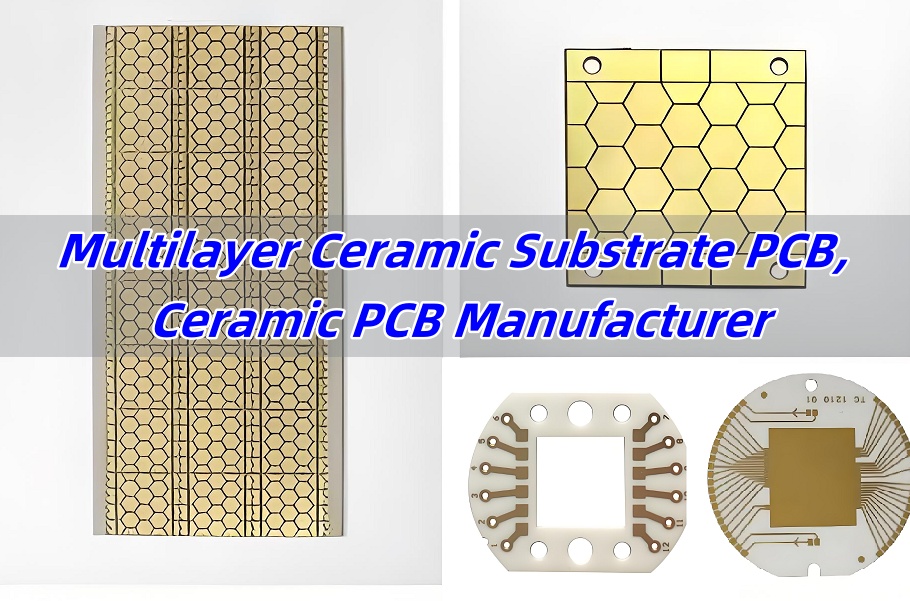
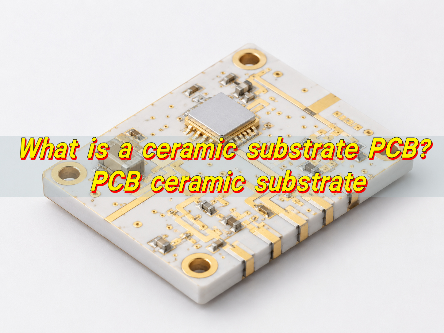
What is a ceramic substrate for PCB?
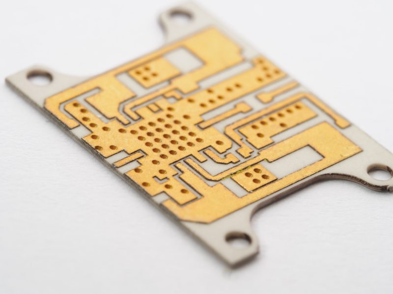
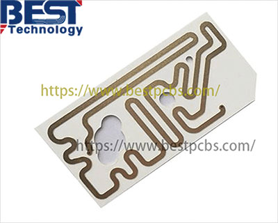
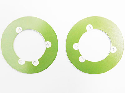
Ceramic substrate for PCB refers to a specialized base material made from advanced ceramic compounds, designed to support and interconnect electronic components. Unlike conventional fiberglass-based laminates such as FR-4, ceramic substrates are engineered to deliver exceptional thermal stability, electrical insulation, and mechanical strength under demanding conditions.
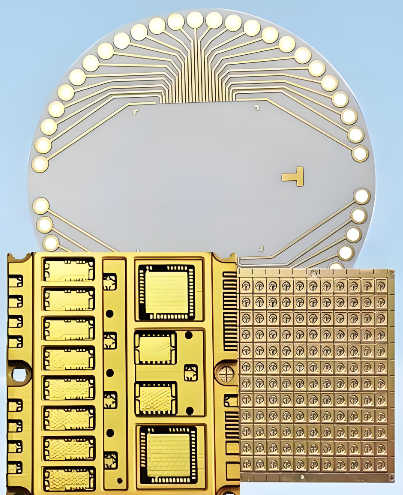
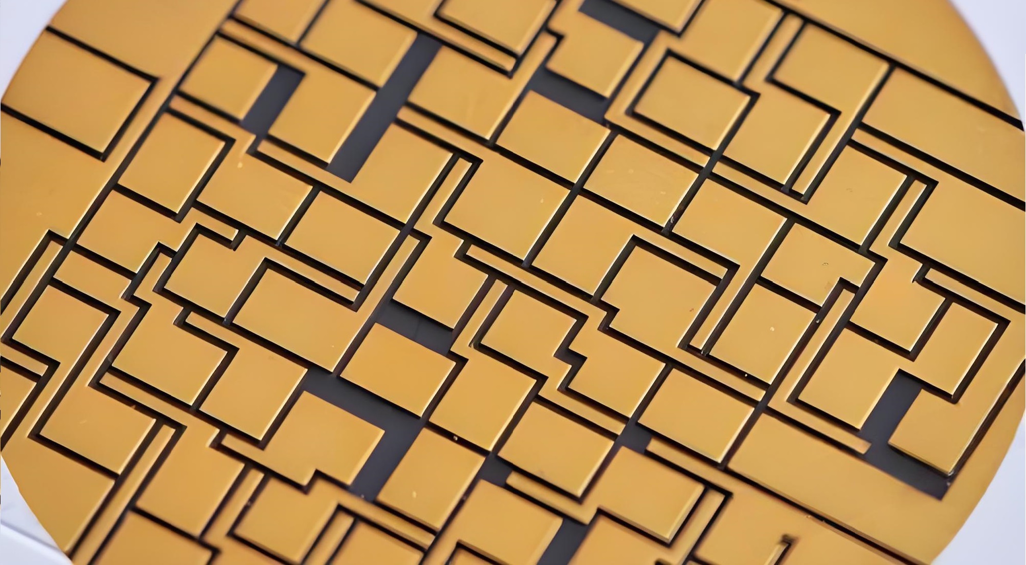
In practical terms, a ceramic substrate circuit board is typically constructed using thick-film or thin-film processes. Conductive traces are printed or deposited directly onto the ceramic surface, forming highly reliable electrical pathways. These boards are often used in applications where heat management, reliability, and dimensional stability are critical—such as power electronics, RF modules, and high-frequency communication systems.
From a design perspective, ceramic substrates offer a level of precision that is difficult to match with organic materials. Their low coefficient of thermal expansion (CTE) aligns closely with semiconductor devices, reducing mechanical stress during thermal cycling. This makes them particularly suitable for chip-on-board (COB) and direct die attachment configurations.
EBest Circuit (Best Technology), with its extensive experience in advanced PCB manufacturing, integrates ceramic substrate solutions into high-performance electronic assemblies. By combining precision fabrication techniques with strict quality control, We ensure that ceramic PCB substrates meet the rigorous demands of modern electronics.
What Materials Are Used for Ceramic Substrates PCB?
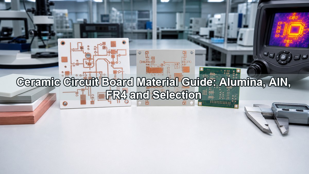
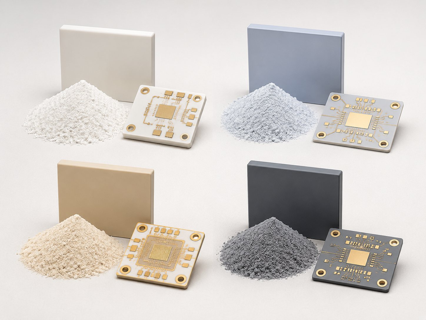
Ceramic substrate PCBs rely on a range of engineered ceramic materials, each selected based on performance requirements such as thermal conductivity, dielectric constant, and mechanical robustness. The most commonly used materials include:
- Aluminum Oxide (Al₂O₃)
Often referred to as alumina, this is the most widely used ceramic substrate material due to its cost-effectiveness and reliable performance. It provides good electrical insulation and moderate thermal conductivity, making it suitable for general-purpose applications. - Aluminum Nitride (AlN)
Known for its exceptional thermal conductivity, aluminum nitride is ideal for high-power and heat-sensitive applications. It offers a thermal performance comparable to some metals while maintaining excellent electrical insulation. - Beryllium Oxide (BeO)
This material delivers outstanding thermal conductivity but is less commonly used due to handling concerns. It is typically reserved for specialized, high-performance applications. - Silicon Nitride (Si₃N₄)
Silicon nitride combines high mechanical strength with good thermal properties. It is particularly valued in applications requiring resistance to thermal shock and mechanical stress.
Each material brings a distinct set of advantages. For instance, alumina offers affordability and reliability, while aluminum nitride excels in thermal management.
In advanced manufacturing environments like those at EBest Circuit, material selection is guided by both engineering analysis and real-world application experience. This ensures that each ceramic PCB substrate is optimized for its intended use.
What are the substrates for PCB?
Printed circuit boards can be built on a variety of substrate materials, each designed to meet different electrical, thermal, and mechanical requirements.
The most common PCB substrate types include:
- FR-4 (Fiberglass Epoxy)
The industry standard for general electronics, offering a balance of cost and performance. - Metal Core PCBs (MCPCB)
Incorporate a metal base (usually aluminum) to improve heat dissipation. - Flexible Substrates (Polyimide)
Used in applications requiring bending or dynamic movement. - Rogers and High-Frequency Laminates
Designed for RF and microwave applications with controlled dielectric properties. - Ceramic Substrates
Provide superior thermal conductivity, electrical insulation, and dimensional stability.
To better understand how ceramic substrates compare with traditional materials, the following table provides a clear overview:
| Property | FR-4 | Metal Core PCB | Ceramic Substrate PCB |
|---|---|---|---|
| Thermal Conductivity | Low | Moderate | High |
| Dielectric Stability | Moderate | Moderate | Excellent |
| Mechanical Strength | Good | Good | Very High |
| Operating Temperature | Limited | Improved | Extremely High |
| Cost | Low | Medium | Higher |
| Reliability | Standard | Enhanced | Premium |
Ceramic substrate PCBs distinguish themselves by delivering a unique combination of thermal and electrical performance. While they may involve higher upfront costs, their long-term reliability and efficiency often justify the investment.
How Does a Ceramic Substrate PCB Help with Heat Dissipation?
Heat management is one of the most compelling reasons to choose a ceramic substrate PCB. As electronic devices become more compact and powerful, efficient heat dissipation is no longer optional—it is essential for performance and longevity.
Ceramic materials inherently possess high thermal conductivity, allowing heat to spread rapidly across the substrate. This prevents localized hotspots, which can degrade components and reduce system reliability.
Several mechanisms contribute to the superior thermal performance of ceramic PCB substrates:
- Direct Heat Conduction
Heat generated by components is transferred directly into the ceramic substrate and distributed evenly. - Low Thermal Resistance
Ceramic materials minimize resistance to heat flow, enabling efficient thermal transfer. - Stable Thermal Expansion
Matching CTE between the substrate and components reduces stress and improves heat cycling performance. - Integration with Heat Sinks
Ceramic substrates can be easily paired with external cooling solutions for enhanced thermal management.
Compared to traditional PCBs, ceramic substrates eliminate the need for additional thermal management layers or complex cooling structures. This not only simplifies design but also reduces overall system weight and footprint.
EBest Circuit leverages these advantages by offering precision-engineered ceramic PCB solutions tailored for high-power applications. Their manufacturing expertise ensures consistent thermal performance across production batches.
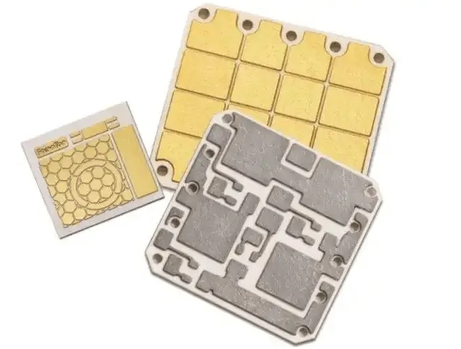
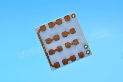
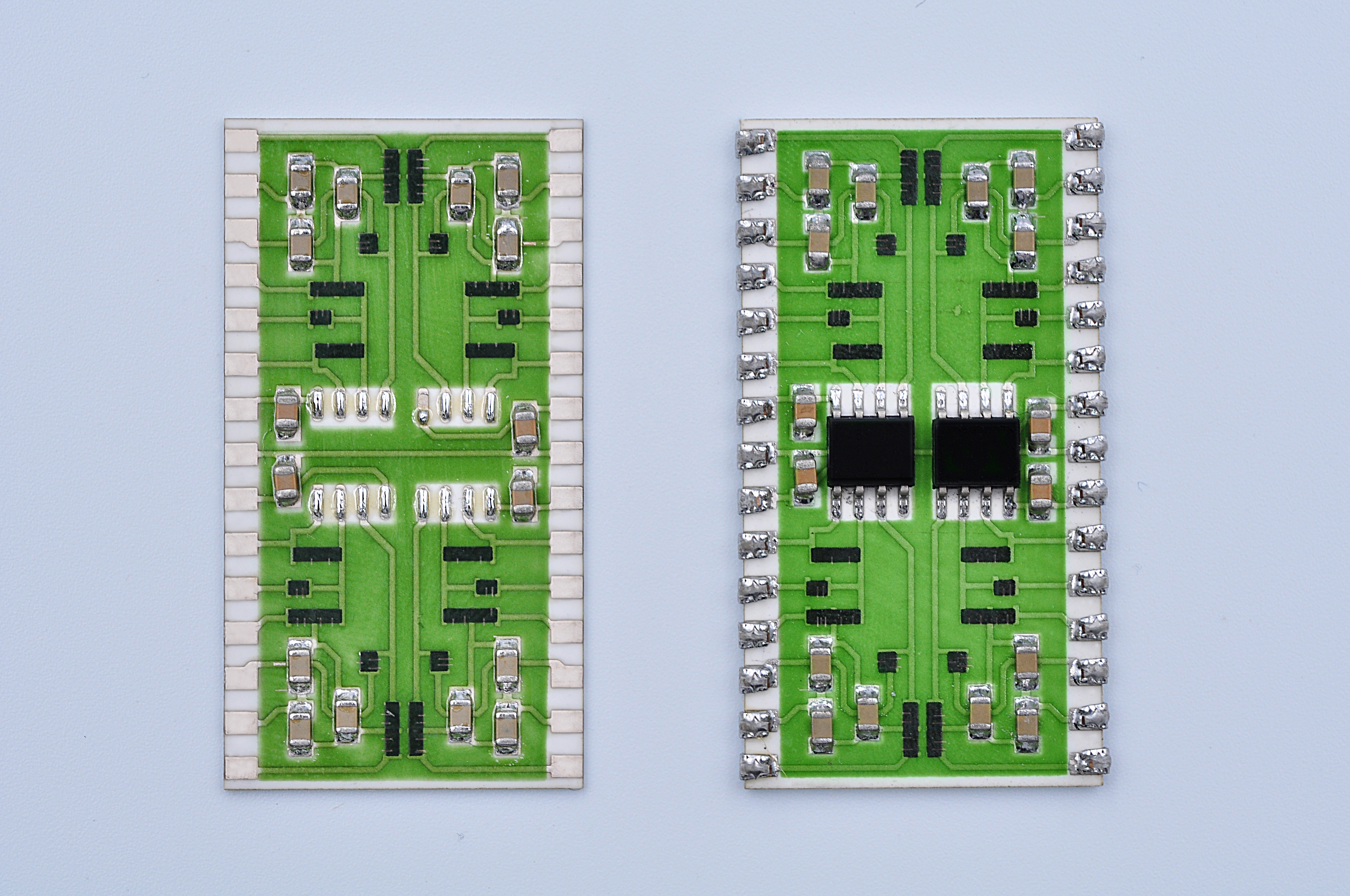
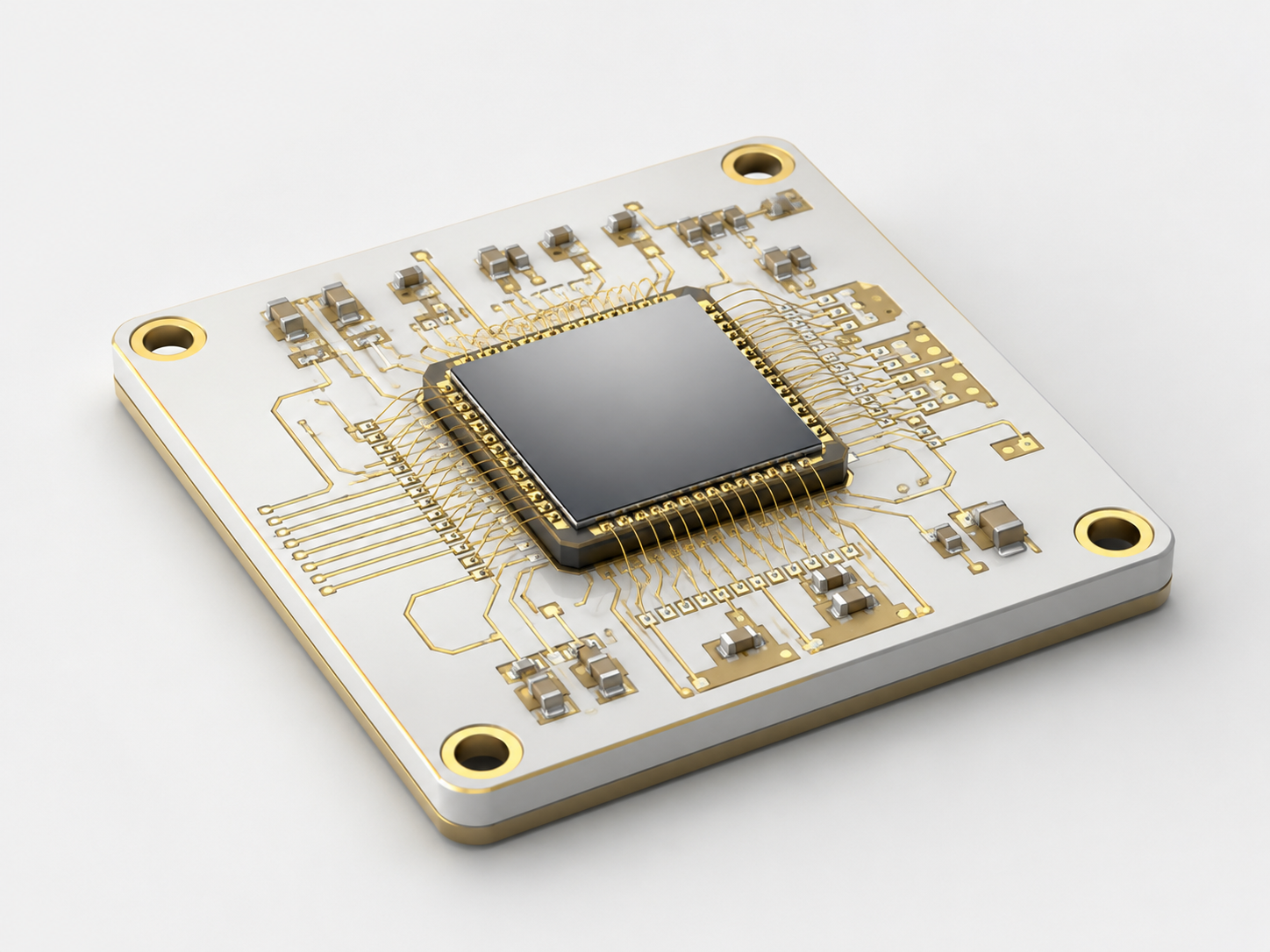
What features does COB ceramic substrate PCB possess?
COB (Chip-On-Board) ceramic substrate PCBs represent a highly integrated approach to electronic assembly. In this configuration, semiconductor chips are mounted directly onto the ceramic substrate, eliminating the need for traditional packaging.
This design approach offers several distinctive features:
- Compact Integration
Direct chip attachment reduces size and improves signal integrity. - Enhanced Thermal Pathways
Heat is transferred directly from the chip to the ceramic substrate. - Improved Electrical Performance
Shorter interconnections minimize signal loss and latency. - High Reliability
Fewer interconnect points reduce the risk of failure. - Precision Alignment
Ceramic substrates provide a stable platform for accurate chip placement.
COB ceramic substrate PCBs are widely used in LED modules, sensors, and high-frequency devices. Their ability to combine compactness with performance makes them a preferred choice for advanced electronic systems.
At EBest Circuit, COB ceramic substrate solutions are developed with a focus on reliability and manufacturability. Their process control ensures consistent bonding quality and optimal performance.
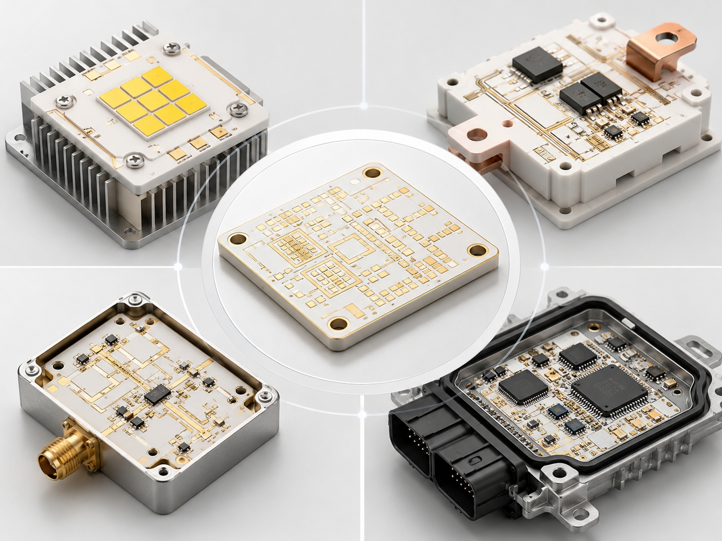
What are ceramic PCBs used for?
Ceramic PCBs are deployed across a wide range of industries where performance and reliability are critical. Their unique properties make them indispensable in applications that demand high thermal efficiency and electrical precision.
Common applications include:
- Power Electronics
Used in inverters, converters, and power modules. - LED Lighting Systems
Provide efficient heat dissipation for high-brightness LEDs. - Automotive Electronics
Suitable for harsh environments and high-temperature conditions. - Telecommunications
Ideal for RF and microwave circuits. - Medical Devices
Ensure reliability in critical healthcare equipment. - Aerospace and Defense
Deliver performance under extreme conditions.
These applications highlight the versatility of ceramic substrate PCBs. Whether in consumer electronics or mission-critical systems, they offer a dependable foundation for advanced circuitry.
What Are the Benefits of Ceramic Substrate PCBs?
Ceramic substrate PCBs deliver a compelling set of advantages that make them a preferred choice for high-performance applications. Their benefits extend beyond basic functionality, offering long-term value and reliability.
Key benefits include:
- Exceptional Thermal Management
Efficient heat dissipation enhances component lifespan. - High Electrical Insulation
Prevents leakage and ensures stable operation. - Dimensional Stability
Maintains structural integrity under temperature variations. - Chemical Resistance
Resists corrosion and environmental degradation. - High-Frequency Performance
Supports fast signal transmission with minimal loss. - Long Service Life
Reduces maintenance and replacement costs.
These advantages translate into improved system performance and reduced operational risks. For engineers and designers, ceramic PCBs provide a reliable platform for innovation.
EBest Circuit integrates these strengths into their manufacturing processes, delivering ceramic PCB substrates that meet stringent industry standards. Our commitment to quality ensures consistent performance across applications.
What is a major disadvantage of ceramics?
While ceramic substrate PCBs offer numerous benefits, it is important to acknowledge their limitations to make informed design decisions.
The primary disadvantage is cost. Ceramic materials and manufacturing processes are generally more expensive than traditional PCB technologies. This can impact project budgets, especially for large-scale production.
Additionally, ceramics can be brittle, making them more susceptible to mechanical damage if not handled properly. However, modern engineering techniques have significantly improved their durability.
Despite these challenges, the advantages of ceramic substrates often outweigh the drawbacks in high-performance applications. When reliability and efficiency are priorities, ceramic PCBs remain a strong choice.
FAQs About Ceramic Substrate PCB
1. Is ceramic substrate PCB better than FR-4?
It depends on the application. Ceramic PCBs outperform FR-4 in thermal and high-frequency scenarios, while FR-4 remains suitable for cost-sensitive designs.
2. Can ceramic PCBs be used in consumer electronics?
Yes, especially in devices requiring efficient heat management, such as LED lighting and power modules.
3. Are ceramic substrates environmentally stable?
They offer excellent resistance to moisture, chemicals, and temperature variations.
4. What industries benefit most from ceramic PCBs?
Automotive, aerospace, telecommunications, and medical industries are among the primary users.
5. How does EBest Circuit ensure quality?
Through strict process control, advanced manufacturing techniques, and adherence to international standards.
Summary:
Ceramic substrate PCBs represent a powerful evolution in circuit board technology. By replacing traditional organic materials with advanced ceramics, they deliver superior thermal performance, electrical stability, and long-term reliability. From power electronics to aerospace systems, their applications continue to expand as technology demands higher efficiency and durability.
For inquiries or technical support, feel free to reach out: sales@bestpcbs.com