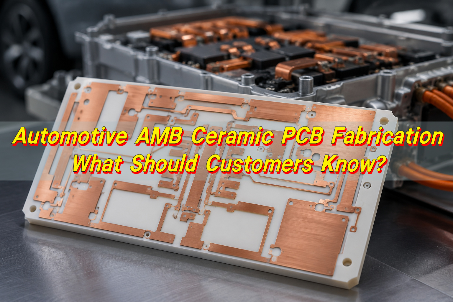
automotive amb ceramic pcb fabrication is used when an automotive power electronics design needs a ceramic substrate that can carry high current, transfer heat away from power devices, and survive repeated thermal and mechanical stress. In practical sourcing terms, buyers should evaluate AMB only when the power module, inverter, converter, or high-load control unit needs stronger copper-to-ceramic bonding than a standard PCB stack can provide.
AMB stands for active metal brazing. In an AMB ceramic substrate, copper is bonded to ceramic using an active brazing process, often under high temperature and controlled atmosphere or vacuum conditions.
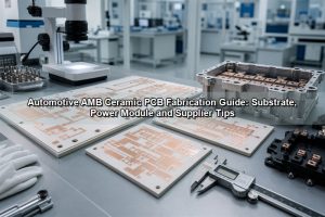
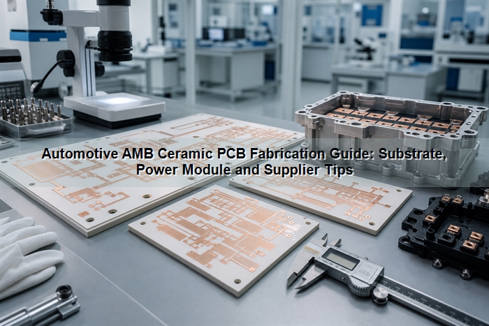
What Is Automotive AMB Ceramic PCB Fabrication?
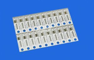
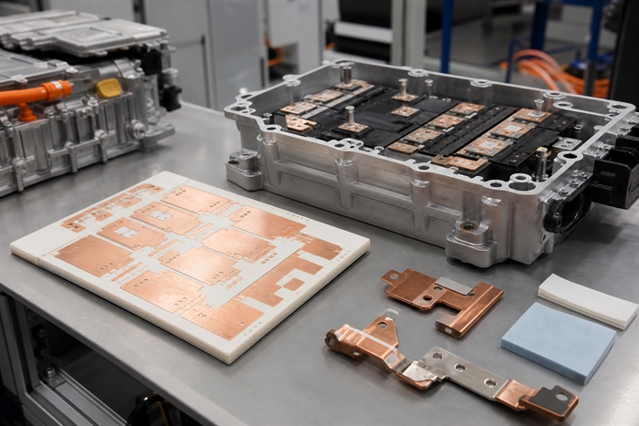
Automotive AMB ceramic PCB fabrication is the production of copper-bonded ceramic substrates for vehicle power electronics, especially where high current, insulation, heat spreading, and thermal cycling resistance must be reviewed together. The process creates a metalized ceramic circuit carrier rather than a conventional organic laminate PCB.
In the fabrication flow, the supplier reviews the drawing, ceramic type, copper thickness, conductor pattern, isolation distance, surface finish, edge tolerance, and sample quantity before confirming the route. For automotive projects, the review should also include thermal cycling expectations, partial discharge or dielectric requirements when applicable, and whether the prototype must represent the future production process.
Compared with standard FR4 PCB or metal-core PCB, AMB is usually considered for higher-power sections of the system, not low-power control electronics. It belongs in the same decision space as ceramic PCB, DBC ceramic substrates, and other power electronic substrate technologies.
Why Are AMB Ceramic Substrates Used in Automotive Power Modules?
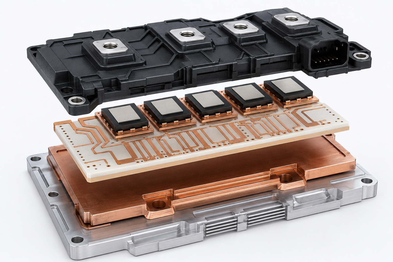
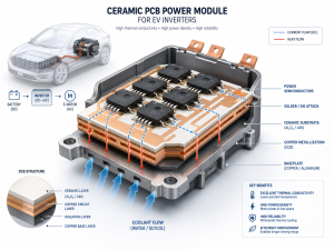
AMB ceramic substrates are used in automotive power modules because they combine electrical insulation, heat transfer, copper current paths, and stronger copper-to-ceramic bonding for harsh power cycling conditions. This matters most when the module carries IGBT, SiC MOSFET, diode, or power-dense switching components in an EV inverter, DC-DC converter, onboard charger, or motor control unit.
The core design logic is stress management. Power devices heat and cool quickly, while copper, ceramic, solder, die attach, and baseplate materials expand differently. If the substrate cannot manage this mismatch, the module may suffer copper delamination, ceramic cracking, solder fatigue, increased thermal resistance, or early electrical failure.
AMB is not necessary for every automotive PCB component. Low-current sensor boards, control boards, lighting controllers, and communication boards may use FR4, high-Tg FR4, rigid-flex, or MCPCB depending on temperature and mechanical requirements. AMB becomes relevant when the circuit carrier is part of the thermal and mechanical reliability path of the power module.
How Does AMB Ceramic Compare with DBC and DPC?
The choice between AMB, DBC, and DPC should start with power density, copper thickness, line resolution, material, and thermal cycling risk. AMB is often considered when mechanical reliability and copper bonding strength matter more than very fine conductor geometry.
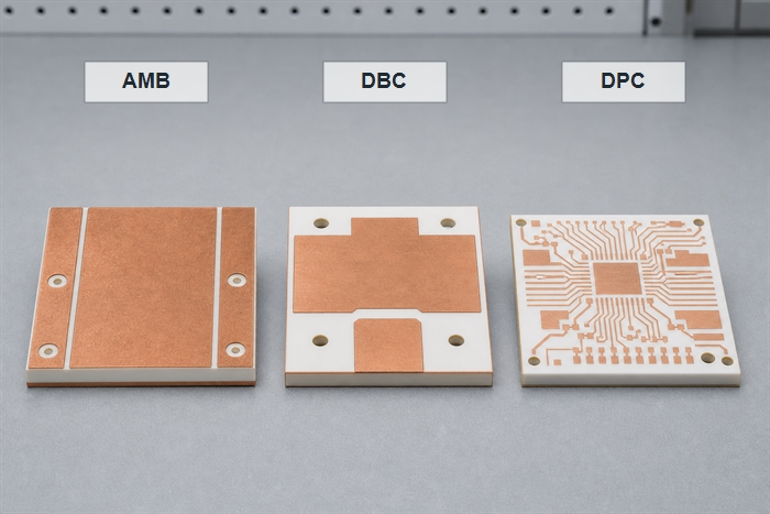
| Technology | Best fit | Buyer should check |
| AMB ceramic substrate | High-reliability power modules, especially with Si3N4 or demanding thermal cycling | Brazing quality, copper adhesion, ceramic toughness, voids, and thermal cycling data |
| DBC / DCB ceramic substrate | Mature power module designs that need thick copper and strong heat spreading | Ceramic type, copper thickness, etching limits, dielectric strength, and solderability |
| DPC ceramic PCB | Finer conductor patterns, smaller features, or designs needing plated structures | Line width, via structure, plating thickness, and whether current capacity is sufficient |
If the design combines high current, thick copper, and severe thermal cycling, AMB or DBC should usually be evaluated before DPC. If the design needs finer routing and lower current, DPC may be more practical. For an RFQ, ask the supplier to explain the process recommendation instead of quoting only the requested keyword.
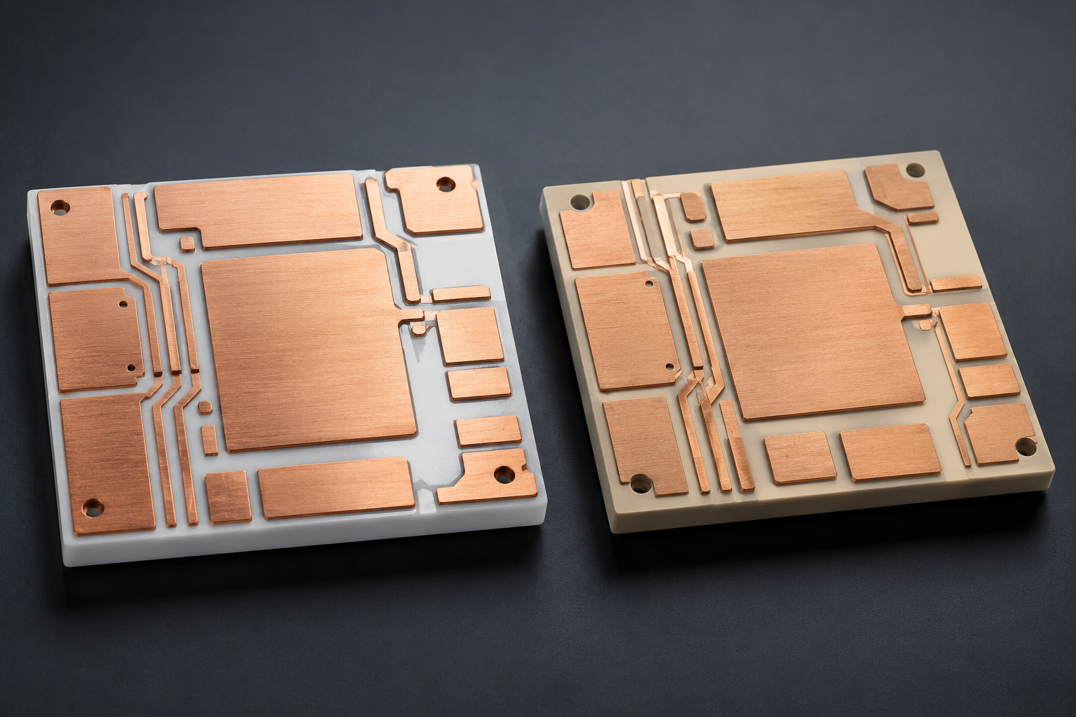
Which Materials Matter in AMB Ceramic PCB Fabrication?
The main materials in AMB ceramic PCB fabrication are the ceramic substrate, copper layer, active brazing material, and final surface finish. For automotive power modules, the ceramic choice can affect thermal conductivity, bending strength, fracture toughness, dielectric behavior, and long-term cycling performance.
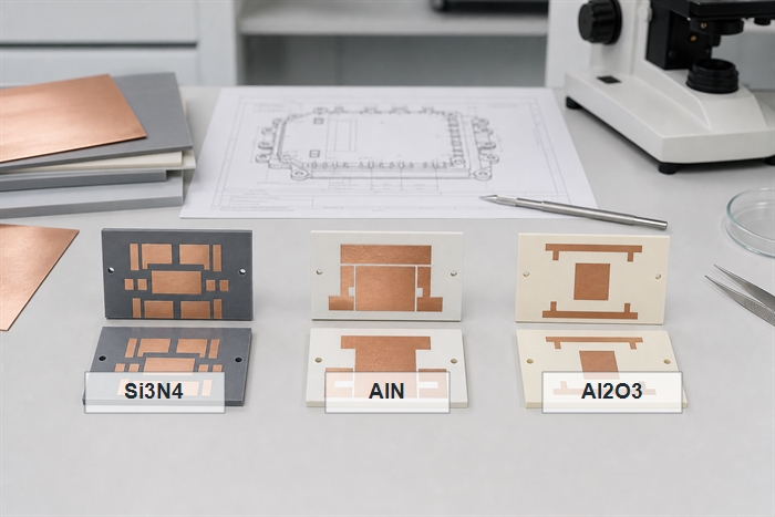
| Material | Why buyers consider it | Practical caution |
| Si3N4 | Often selected for higher mechanical toughness and thermal cycling resistance in demanding power modules | Cost, availability, thickness, and supplier process maturity should be confirmed early |
| AlN | Selected when high thermal conductivity is a primary driver | Mechanical robustness and cycling performance must be reviewed with the exact module design |
| Al2O3 | Useful when cost and insulation matter more than maximum thermal performance | May not be enough for high-power automotive modules with aggressive heat density |
For high-risk automotive applications, do not choose only by thermal conductivity. A substrate with higher thermal conductivity but lower mechanical margin may still create reliability risk if the copper thickness, die attach, baseplate, and thermal cycling profile are not matched.
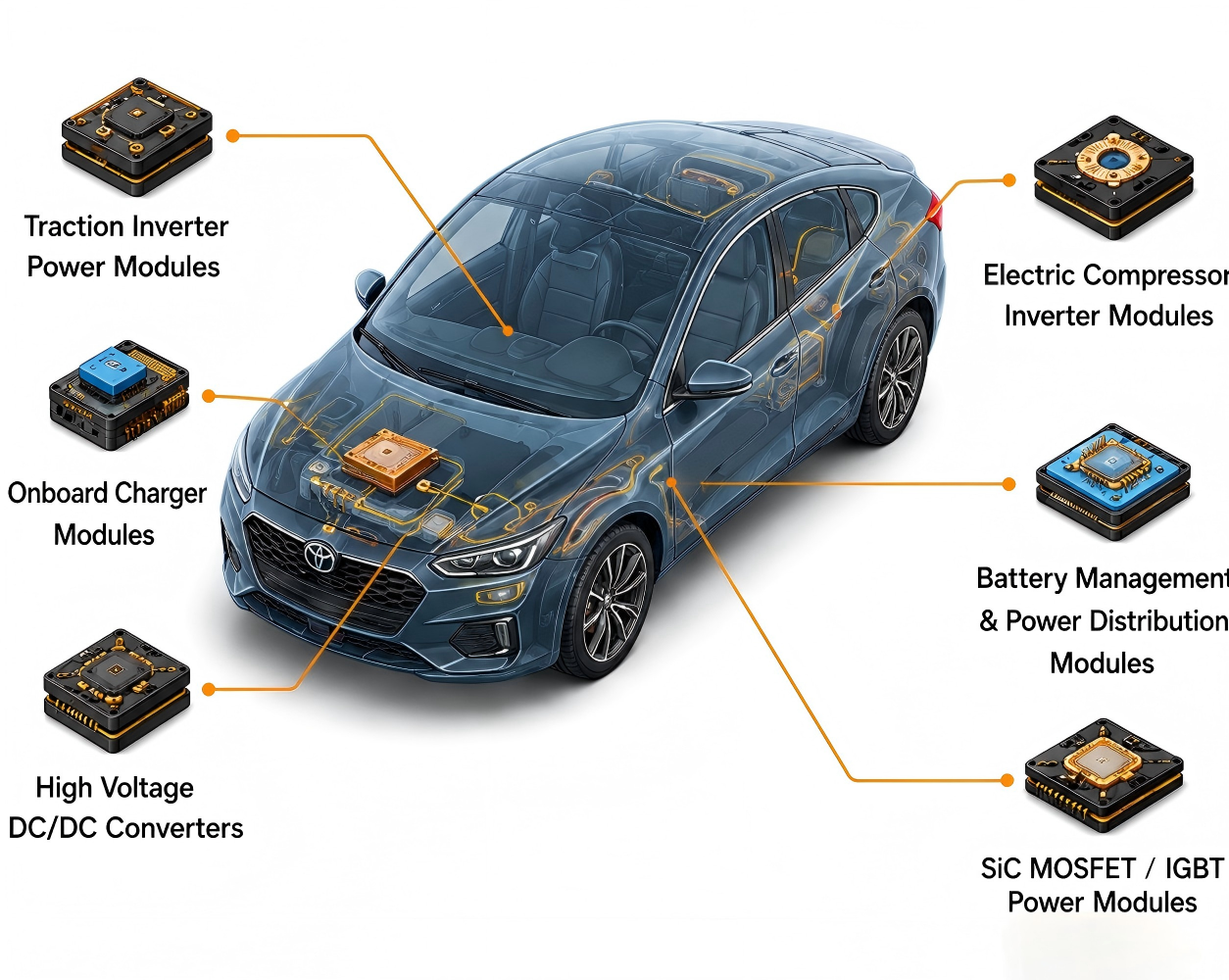
What Automotive PCB Components Use AMB Ceramic Substrates?
AMB ceramic substrates are mainly used in automotive power electronics components where the circuit carrier is exposed to high heat flux, high current, and repeated load changes. They are less relevant for ordinary logic boards and more relevant for modules that sit close to power semiconductor devices.
- EV traction inverter power modules using SiC MOSFETs, IGBTs, or diodes.
- Onboard charger power conversion modules.
- DC-DC converter modules for high-voltage to low-voltage conversion.
- Motor control modules and high-load switching units.
- Battery thermal management or high-current protection circuits when ceramic isolation and heat spreading are needed.
For mixed automotive PCB assemblies, the AMB substrate is often only one part of the full electronic system. The surrounding gate driver, sensing, communication, and control circuits may still use conventional PCB or PCBA processes, so the supplier handoff between ceramic substrate fabrication and assembly review should be planned early.
What Manufacturing Factors Affect AMB Ceramic PCB Quality?
AMB ceramic PCB quality is strongly affected by ceramic preparation, copper thickness, brazing interface quality, pattern etching, surface finish, edge processing, and inspection. A buyer should review these factors before approving a prototype because they influence both electrical performance and long-term mechanical reliability.
- Copper thickness: affects current carrying capacity, heat spreading, etching geometry, and stress at the copper-to-ceramic interface.
- Pattern geometry: sharp corners, narrow gaps, large copper islands, and asymmetric copper balance can change stress concentration.
- Brazing interface: voids, poor wetting, or inconsistent bonding can increase thermal resistance and reduce cycling life.
- Ceramic edge quality: chips, microcracks, and rough edges can create handling and reliability risk.
- Surface finish: should match die attach, soldering, wire bonding, or module assembly requirements.
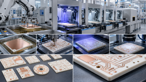
EBest Circuit (Best Technology) lists AMB ceramic PCB among its ceramic PCB technology scope, together with DPC, DBC/DCB, LTCC, HTCC, thick-film, and thin-film ceramic PCB. For automotive use, any maximum capability or fast-turn request should still be checked against material, dimensions, copper thickness, testing scope, and engineering review.
What Reliability Tests Matter for Automotive AMB Ceramic PCB?
Reliability testing for automotive AMB ceramic PCB should focus on thermal cycling, power cycling relevance, insulation, copper adhesion, dimensional stability, solderability, and visual or microstructural inspection. The exact test plan should match the module’s voltage class, mission profile, assembly method, and customer qualification standard.
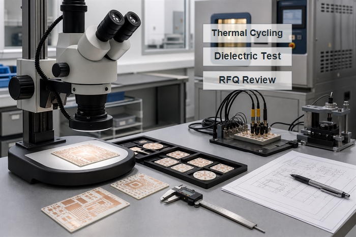
| Check | Why it matters | Buyer action |
| Thermal cycling | Finds stress-related issues at the copper, braze, ceramic, and solder interfaces | Share the expected temperature range and cycle target before quoting |
| Dielectric / insulation testing | Confirms isolation margin for high-voltage automotive modules | Specify voltage, spacing, and acceptance criteria |
| Microsection or interface review | Helps evaluate voids, bonding quality, copper thickness, and process consistency | Request sample inspection data for critical prototype builds |
| Dimensional inspection | Protects module fit, die placement, and baseplate alignment | Mark critical dimensions separately from non-critical dimensions |
For SiC traction inverter modules, power cycling is especially relevant because it stresses the package under realistic electrical and thermal load changes. Even when the AMB supplier does not run full module-level power cycling, the substrate design should be reviewed with that stress path in mind.
What Should Buyers Provide for an AMB Ceramic PCB Quote?
A useful AMB ceramic PCB quote requires more than Gerber files. The supplier needs enough design and application context to judge material fit, copper thickness, brazing route, test requirements, and whether the prototype can scale to automotive production.
- Gerber, drill, drawing, and copper layer data.
- Ceramic material preference, such as Si3N4, AlN, or Al2O3.
- Copper thickness, substrate thickness, and finished board thickness.
- Surface finish and assembly method, including soldering, die attach, or wire bonding needs.
- Voltage, current, insulation distance, and thermal load targets.
- Critical dimensions, tolerance class, and edge quality requirements.
- Prototype quantity, expected production volume, and PPAP or automotive documentation expectations.
- Required inspection reports, thermal cycling requirements, and packaging instructions.
If the project includes assembled automotive PCB components, send BOM, placement data, thermal interface notes, and test requirements at the same time. This lets the supplier check substrate fabrication and downstream assembly risks together instead of discovering mismatches after samples are made.
How to Choose Automotive PCB Suppliers for AMB Ceramic Projects?
Automotive PCB suppliers for AMB ceramic projects should be evaluated by engineering review quality, ceramic substrate experience, inspection capability, documentation discipline, and ability to support prototype-to-production transfer. A supplier that can quote quickly but cannot explain material trade-offs may create risk during qualification.
Ask each supplier how they review Si3N4 versus AlN, which copper thicknesses fit the selected process, what inspection data can be provided for prototypes, how they control edge damage, and what information is needed before mass production. If automotive documentation is required, confirm expectations before the prototype order, not after the design is frozen.
EBest Circuit (Best Technology) can be positioned as a ceramic PCB and PCBA manufacturing partner for buyers who need engineering communication across prototype review, ceramic substrate fabrication, assembly discussion, and quotation preparation. For AMB projects, the useful conversation is not a generic price request; it is a file-and-requirement review that connects material choice, reliability target, and production feasibility.
FAQ
What is AMB ceramic PCB fabrication used for in automotive electronics?
AMB ceramic PCB fabrication is used for high-power automotive electronics where the substrate must provide insulation, heat spreading, copper current paths, and thermal cycling resistance. Typical uses include EV inverter power modules, onboard chargers, DC-DC converters, motor control modules, and other circuits that place SiC MOSFETs, IGBTs, or diodes close to the heat path.
Is AMB ceramic better than DBC for automotive power modules?
AMB is not automatically better than DBC; it is better suited when the design needs stronger copper-to-ceramic bonding and improved mechanical reliability under severe thermal cycling. DBC remains a mature option for many power modules. The correct choice depends on ceramic material, copper thickness, module stress profile, cost target, and qualification requirements.
Which ceramic material is best for AMB power modules?
Si3N4 is often considered for demanding AMB power modules because it offers strong mechanical toughness and thermal cycling resistance. AlN is attractive when thermal conductivity is the main driver, while Al2O3 is more cost-oriented but usually less suitable for high-power automotive modules. Buyers should review material choice with copper thickness, module layout, and test requirements together.
What files are needed for an automotive AMB ceramic PCB quote?
A useful quote should include Gerber data, mechanical drawings, ceramic material preference, copper thickness, substrate thickness, surface finish, voltage and current targets, thermal load, critical tolerances, sample quantity, production estimate, and reliability test expectations. If assembly is involved, include BOM, placement data, die attach or soldering notes, and packaging requirements.
Can AMB ceramic substrates be assembled into automotive power modules?
Yes, AMB ceramic substrates can be used in automotive power module assembly, but the assembly method must be reviewed early. Die attach, solderability, wire bonding, surface finish, baseplate attachment, insulation spacing, and thermal interface materials can all affect reliability. The substrate supplier and assembly team should align before prototype approval.
How should buyers evaluate automotive PCB suppliers for AMB ceramic projects?
Buyers should evaluate whether the supplier can review ceramic material, copper thickness, AMB process route, edge quality, inspection data, thermal cycling expectations, and prototype-to-production transfer. For automotive projects, also check documentation discipline, traceability expectations, quality system fit, and whether the supplier can explain trade-offs instead of only quoting a price.
Conclusion
Automotive AMB ceramic PCB fabrication is most useful when the design needs a ceramic power substrate for high current, heat spreading, insulation, and thermal cycling reliability. It is not the default choice for every automotive PCB; it should be selected when the power module’s stress profile, device type, copper requirement, and qualification plan justify the process.
Before requesting a quote, prepare the material target, copper thickness, drawings, electrical and thermal requirements, prototype quantity, expected production volume, and reliability test expectations. If you are evaluating AMB ceramic substrates for automotive power modules, contact EBest Circuit (Best Technology) at sales@bestpcbs.com for engineering review and quotation support.