PCB manufacturing PCB manufacturing
Home > Blog

multilayer ceramic pcb

Multilayer Ceramic Circuit Board: What Should Engineers Know?
Tuesday, May 19th, 2026

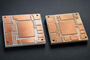
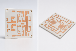
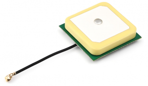
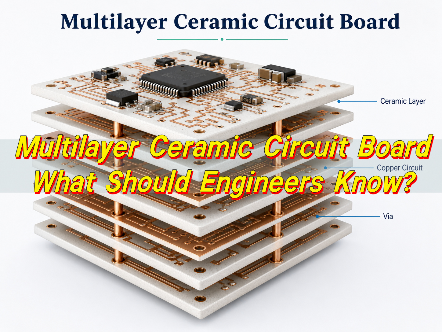
What Is a Multilayer Ceramic Circuit Board?

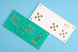
Multilayer Ceramic Circuit Board is a circuit structure built with multiple conductive layers inside or on a ceramic substrate. Instead of using glass-reinforced epoxy, like a standard FR4 board, it uses ceramic materials such as alumina, aluminum nitride, silicon nitride, or low-temperature co-fired ceramic materials. These materials give the board strong thermal performance, stable electrical behavior, and excellent mechanical reliability in demanding applications.

A multilayer ceramic substrate is usually designed with several internal layers. These layers may include signal traces, ground planes, power planes, buried vias, thermal vias, and pads for components. The internal structure allows engineers to place more circuits into a smaller area while keeping the board stable and efficient. Compared with a single-layer ceramic board, the multilayer version offers more design freedom and better electrical integration.

The term “multilayer ceramics” can refer to different technologies. Some boards are made by stacking ceramic green sheets and co-firing them with metal paste. Others use post-fired ceramic substrates with plated copper structures. The right technology depends on the required line width, copper thickness, thermal conductivity, operating frequency, and production volume.

How Does a Multilayer Ceramic PCB Work?

Multilayer ceramic PCB works by combining several conductive layers with insulating ceramic layers. Each conductive layer has a specific electrical role. Some layers carry signals, some distribute power, and some act as ground planes.

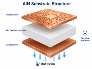
The ceramic material acts as the dielectric body. It separates the copper, tungsten, molybdenum, silver, or gold conductor layers while providing electrical insulation. At the same time, ceramic conducts heat better than many organic PCB materials. This allows heat generated by power devices, LEDs, resistors, or RF components to move away from hot spots more efficiently.

In high-speed or RF designs, the ceramic substrate also helps keep electrical performance stable. Ceramic materials usually have controlled dielectric properties, low moisture absorption, and good dimensional stability. This helps the board maintain signal quality across temperature changes and long-term use.

A typical multilayer ceramic circuit structure may include:

  • Signal layers for routing compact circuits and component connections.
  • Ground layers for shielding, return current control, and noise reduction.
  • Power layers for stable voltage distribution.
  • Via structures for vertical interconnection between layers.
  • Thermal paths for transferring heat from components to the base or housing.

The design principle is simple, but the execution requires precision. The inner layers must align correctly. Via filling must be reliable. The ceramic body must be fired or processed under controlled conditions.

ItemStandard FR4 Multilayer Circuit BoardMultilayer Ceramic Circuit Board
Base MaterialGlass fiber and epoxy resinAlumina, AlN, Si₃N₄, LTCC, or other ceramics
Thermal ConductivityModerateHigh to very high, depending on ceramic type
Dimensional StabilityGood for common electronicsExcellent under heat and harsh use
Moisture AbsorptionHigher than ceramicVery low
Common UseConsumer electronics, control boards, general PCB assembliesPower electronics, RF modules, sensors, medical, automotive, LED, aerospace
Main AdvantageCost efficiency and broad availabilityHeat control, compact structure, high reliability

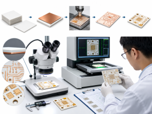
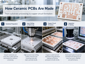
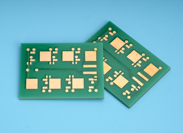
How Is a Multilayer Ceramic Circuit Board Manufactured?

The manufacturing process depends on the selected ceramic technology. However, the general target is always the same: create a stable ceramic body with precise internal conductive layers and reliable vertical interconnections. For this reason, the process requires strict control of materials, layer registration, firing temperature, conductor shrinkage, and surface finish.

For LTCC and HTCC structures, production often starts with ceramic green tape. This tape is a flexible ceramic sheet before firing. The manufacturer punches or drills via holes, fills them with conductive paste, prints circuit patterns, stacks the layers, laminates them under pressure, and then fires the structure at a controlled temperature. During firing, the ceramic and conductor system become a solid integrated body.

For post-fired ceramic PCB manufacturing, the ceramic substrate may be prepared first, and then copper circuits are built by metallization, plating, etching, or film deposition. This route is often used when higher copper conductivity or thicker copper is needed.

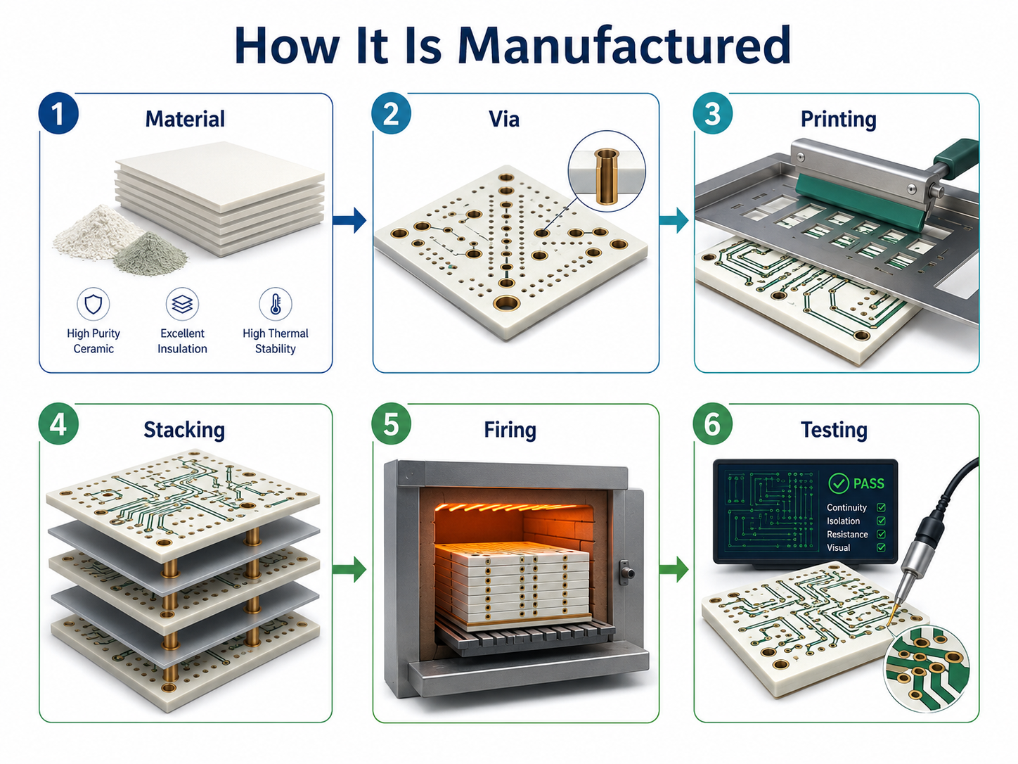
A common multilayer ceramic PCB manufacturing flow may include:

  • Material selection: Choose alumina, AlN, Si₃N₄, LTCC, or another ceramic based on heat, dielectric, and mechanical needs.
  • Stack-up design review: Confirm layer count, conductor width, spacing, via size, dielectric thickness, and thermal path.
  • Via formation: Create vertical holes by punching, laser processing, or drilling, depending on the process.
  • Via filling and conductor printing: Fill vias and print inner circuit layers using suitable conductive material.
  • Layer stacking and alignment: Stack all layers with accurate registration to protect electrical continuity.
  • Lamination or bonding: Press layers together under controlled temperature and pressure.
  • Firing or metallization: Sinter the ceramic body or build copper after ceramic firing.
  • Surface finishing: Apply suitable finish for soldering, wire bonding, or component attachment.
  • Inspection and testing: Use visual inspection, electrical testing, dimensional measurement, and reliability checks.

EBest Circuit (Best Technology) supports ceramic PCB manufacturing with engineering review, material selection, DFM feedback, and production process control. For multilayer ceramic projects, this early review is especially useful because design choices made at the beginning directly affect yield, cost, and long-term product reliability.

What Should Be Considered in Multilayer Circuit Board Design?

Multilayer circuit board design for ceramic substrates requires a slightly different mindset from FR4 design. Engineers should not treat ceramic as just another base material. Ceramic has its own processing rules, strength profile, copper bonding behavior, dielectric behavior, and thermal characteristics.

The first point is material choice. Alumina is widely used because it offers good insulation, stable performance, and attractive cost control. Aluminum nitride is preferred when thermal conductivity is a key requirement. Silicon nitride is useful where mechanical toughness and thermal cycling resistance matter. LTCC materials are often selected for compact RF modules, sensors, and embedded passive designs.

The second point is the layer structure. Engineers should decide which layers will carry signals, which layers will act as ground, and which paths will move heat away from components. In compact power or RF designs, a ground plane is not only an electrical reference. It may also help reduce noise, improve shielding, and stabilize impedance.

Designers also need to consider via diameter, via pitch, conductor thickness, minimum spacing, solder pad size, board thickness, edge clearance, and surface finish. Ceramic is hard and dimensionally stable, which is excellent for many uses.

Here is a practical design comparison:

Design FactorWhy It MattersEngineering Recommendation
Ceramic MaterialAffects heat transfer, dielectric behavior, cost, and strengthSelect material according to power, frequency, size, and environment
Layer CountControls routing density and board thicknessUse only the required number of layers to balance function and cost
Via StructureDetermines vertical connection and current pathMatch via size and filling method with process capability
Ground PlaneImproves signal return path and shieldingUse continuous ground where RF or high-speed signals are present
Thermal PathReduces component temperature risePlace thermal vias or heat-spreading layers close to heat sources
Copper ThicknessAffects current carrying and heat spreadingChoose based on current load and assembly needs
Pad DesignAffects solder quality and component stabilityFollow component footprint and ceramic process rules
Surface FinishAffects solderability and wire bondingSelect ENIG, silver, gold, or other finish based on assembly method

A well-designed multilayer ceramic board is not only smaller. It is also easier to assemble, easier to test, and more reliable in service. Therefore, engineers should involve the manufacturer early, especially when the design includes fine lines, high thermal load, RF routing, or special component packaging.

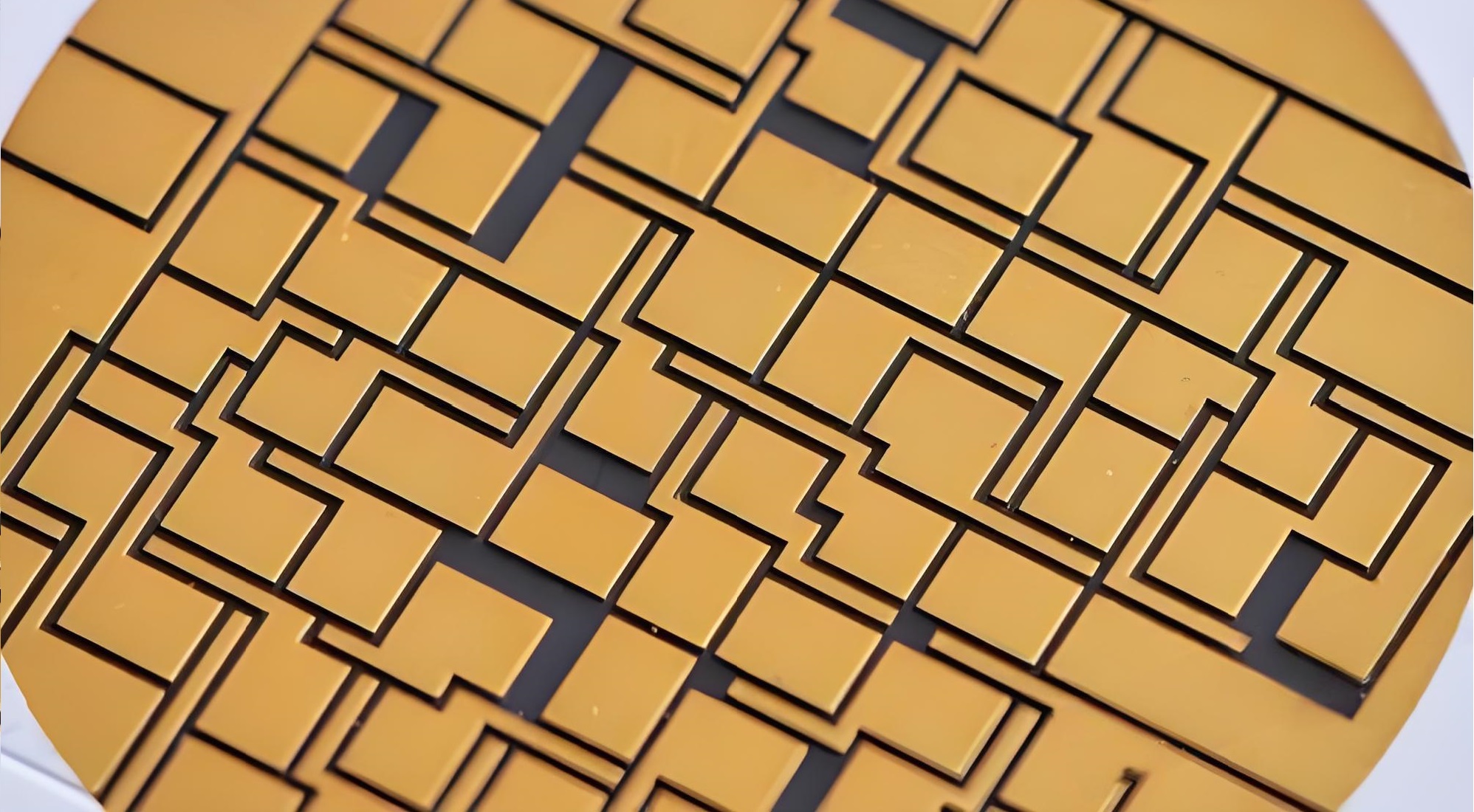
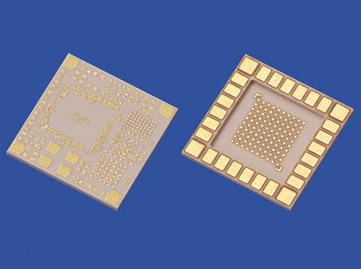
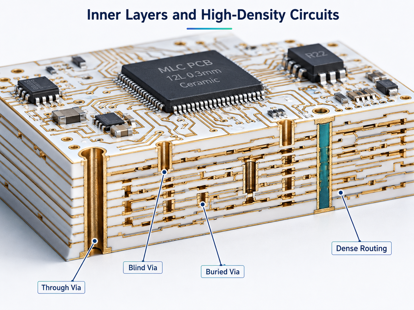
How Are Inner Layers Connected in a Multilayer Ceramic PCB?

Inner layers in a multilayer ceramic PCB are connected through vias. These vias create vertical electrical paths between different conductive layers. Without vias, each layer would remain isolated, and the board could not function as an integrated multilayer circuit.

The via structure may vary according to the ceramic process. In co-fired ceramic technology, vias are usually formed in the green tape before firing. They are then filled with conductive paste. After stacking and firing, the via becomes part of the ceramic body. In plated ceramic processes, vias may be laser-drilled or mechanically processed, then metallized and plated to form a conductive barrel.

There are several via types that may be used in multilayer ceramic designs:

Via TypeDescriptionTypical Use
Through ViaConnects from the top layer to the bottom layerGeneral interconnection and test access
Blind ViaConnects an outer layer to one or more inner layersCompact routing and HDI-style layouts
Buried ViaConnects only internal layersDense routing without occupying outer-layer space
Filled ViaVia hole is filled with conductive or non-conductive materialHeat transfer, current carrying, or flat pad support
Thermal ViaDesigned mainly to move heatPower devices, LEDs, modules, and heat-sensitive circuits

For power electronics, vias must also carry current and heat. A via that only works electrically may not be enough. The designer may need a via array under power components, a copper-filled structure, or direct thermal connection to a metal base or heat sink. In RF circuits, via placement affects grounding and shielding. Poor via distribution can increase parasitic effects, while a carefully designed via fence can improve isolation.

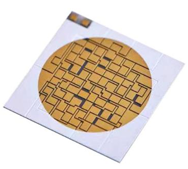
Can Multilayer Ceramic PCBs Support High-Density Circuits?

Yes, multilayer ceramic PCBs can support high-density circuits when the process and design rules are properly matched. Their multilayer structure allows more routing channels within a smaller footprint. This is helpful for compact modules, sensor packages, RF front-end circuits, LED arrays, power control units, and advanced industrial electronics.

High-density design is not only about placing many traces in a small area. It also requires stable insulation, precise via registration, controlled conductor geometry, and reliable assembly pads. Ceramic substrates offer strong dimensional stability, which helps maintain fine features during processing and use.

LTCC is especially useful for compact high-density designs. It can integrate internal conductors, vias, cavities, and sometimes passive structures. This makes it suitable for RF modules, filters, antennas, sensor packages, and compact electronic assemblies.

For dense ceramic circuit boards, engineers should pay attention to:

  • Routing priority: Place sensitive signals first, then power and support traces.
  • Ground control: Use ground planes and via stitching to manage return paths.
  • Thermal mapping: Identify heat sources before finalizing layer placement.
  • Assembly clearance: Keep enough room for soldering, inspection, and rework evaluation.
  • Panelization: Consider breakaway design, edge strength, and handling during production.
  • Testing access: Add test points or inspection features where space allows.

A high-density multilayer ceramic substrate can be powerful when designed with discipline. It can reduce module size while improving heat flow and electrical stability.

What Are the Benefits of Multilayer Ceramic Circuit Boards?

The benefits of multilayer ceramic circuit boards come from the combination of ceramic insulation, dense interconnection, and excellent thermal behavior.

One major benefit is thermal management. Ceramic materials can transfer heat more effectively than many organic PCB materials. Aluminum nitride, in particular, offers high thermal conductivity, making it suitable for power modules, high-brightness LEDs, laser devices, and compact electronics with concentrated heat sources.

Another benefit is electrical stability. Ceramic substrates usually have low moisture absorption and stable dielectric properties. This supports RF performance, high-frequency behavior, and long-term signal integrity. For products working in changing temperatures or demanding environments, that stability is highly valuable.

Mechanical and chemical resistance also matter. Ceramic boards can perform well in high-temperature, high-voltage, or chemically challenging conditions. They keep their shape well and provide a strong platform for precision circuits.

Key benefits include:

  • Efficient heat dissipation for power components and high-brightness devices.
  • Compact multilayer routing for smaller electronic modules.
  • Stable dielectric behavior for RF, sensor, and high-frequency circuits.
  • Low moisture absorption for dependable operation in harsh environments.
  • Strong insulation for high-voltage or high-reliability circuits.
  • Excellent dimensional stability for precise assembly and fine features.
  • Good long-term reliability for automotive, medical, aerospace, and industrial uses.

Compared with a standard multilayer circuit board, ceramic multilayer technology is not always chosen for basic consumer electronics. Its value becomes clear when the application needs heat control, compact design, stable electrical properties, or rugged operation.

What Are the Common Applications of Multilayer Ceramic PCBs?

Multilayer ceramic PCBs are used in applications where performance, space, and reliability are all important. They are especially valuable when the circuit must handle heat, maintain electrical stability, or operate in demanding conditions..

In power electronics, ceramic boards are used for modules, drivers, converters, inverters, and power control systems. The ceramic body helps move heat away from power semiconductors. This supports better operating temperature control and longer component life.

In RF and microwave devices, ceramic materials provide stable dielectric behavior. This makes them suitable for filters, antennas, amplifiers, radar-related modules, communication systems, and high-frequency sensor packages.

In medical electronics, ceramic boards may be used in sensors, diagnostic modules, imaging equipment, wearable devices, and precision control systems. These products often require stable performance, compact design, and dependable insulation.

In automotive and aerospace electronics, ceramic multilayer boards support harsh-environment applications, including power control, sensor systems, lighting, and communication modules.

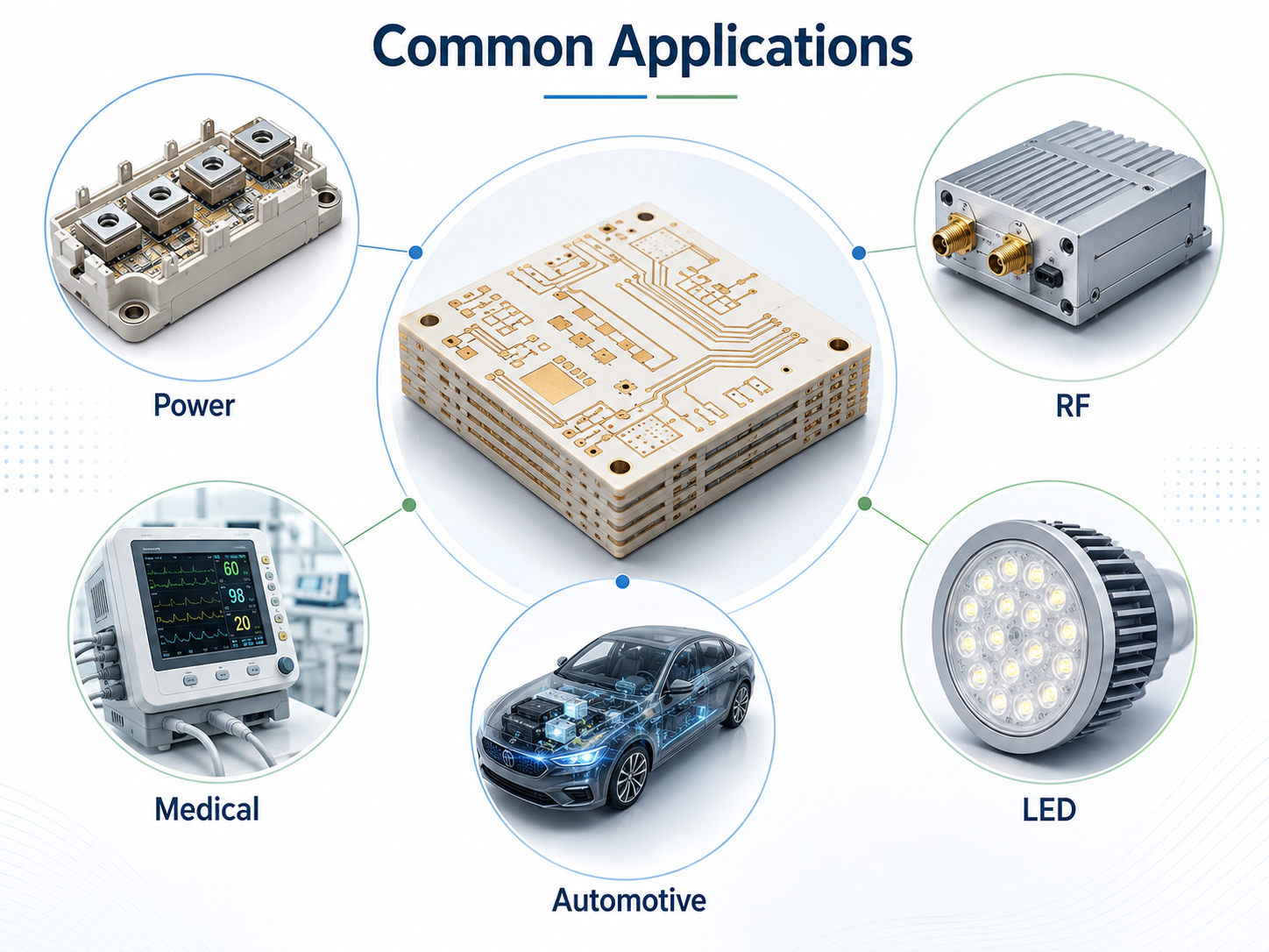
Common application areas include:

  • Power modules and semiconductor packaging.
  • High-brightness LED and laser systems.
  • RF and microwave communication modules.
  • Industrial sensors and control circuits.
  • Medical diagnostic and monitoring equipment.
  • Automotive electronics and EV-related power systems.
  • Aerospace, UAV, and defense-grade electronic modules.
  • High-temperature electronics and precision instruments.

The application range continues to expand because electronics are becoming smaller, hotter, and more function-rich. A multilayer ceramic circuit structure helps engineers fit more capability into limited space while keeping the product stable and manufacturable.

How Do You Choose a Reliable Multilayer Ceramic PCB Manufacturer?

Choosing the right manufacturer is one of the most important decisions in a multilayer ceramic PCB project. Ceramic multilayer boards require more than basic PCB production ability. The manufacturer should understand ceramic materials, stack-up control, via processing, metallization, firing behavior, surface finish, assembly compatibility, and inspection standards.

A reliable manufacturer should first review the design from an engineering perspective. This includes checking material choice, conductor width, spacing, via size, layer count, thermal path, pad design, and expected assembly method. Good DFM feedback can help engineers improve the design before production begins. This saves time and improves first-pass success.

The manufacturer should also have experience with different ceramic materials. Alumina, aluminum nitride, silicon nitride, LTCC, and other multilayer ceramics do not behave the same way during processing. Each material has its own thermal performance, mechanical strength, dielectric value, and processing window.

Quality control is another key factor. Ceramic boards should be inspected for dimensions, layer alignment, circuit continuity, surface quality, plating quality, solderability, and visual defects. For advanced projects, additional checks such as X-ray inspection, cross-section analysis, thermal testing, and reliability testing may be needed.

When evaluating a manufacturer, engineers can use this checklist:

Evaluation PointWhat to CheckWhy It Matters
Ceramic Material CapabilityAlumina, AlN, Si₃N₄, LTCC, DPC, DBC, or other optionsEnsures the right substrate for thermal and electrical needs
Multilayer Process ExperienceLayer alignment, via filling, lamination, firing, metallizationProtects inner-layer reliability
DFM SupportStack-up review, pad review, via review, process adviceReduces design risk before fabrication
Testing CapabilityElectrical test, dimensional inspection, visual inspection, X-ray when neededConfirms product quality before shipment
Assembly KnowledgeSoldering, wire bonding, component placement, thermal interfaceImproves compatibility with PCBA production
Engineering CommunicationClear feedback, fast response, practical suggestionsHelps projects move faster and with fewer revisions
TraceabilityMaterial batch, process record, inspection dataSupports quality control and regulated applications

EBest Circuit (Best Technology) can support customers from ceramic PCB design review to fabrication and assembly-related engineering discussion. For multilayer ceramic projects, the team can help evaluate material options, stack-up feasibility, via structure, surface finish, thermal path, and manufacturing risk. This is especially helpful for engineers working on power electronics, RF modules, medical devices, industrial control systems, LED products, UAV electronics, and high-reliability applications.

For project support or quotation requests, contact sales@bestpcbs.com

You may also like

Multilayer Ceramic Substrate PCB, Ceramic PCB Manufacturer
Tuesday, April 15th, 2025

With nearly two decades of experience, EBest Circuit (Best Technology) has become one of the most reliable ceramic PCB manufacturers in Asia. We specialize in high-quality ceramic substrate PCBs for a wide range of industries. From automotive to aerospace, from LED lighting to power electronics—we support innovation with strong technical backing and fast delivery.

We don’t just offer boards; we offer tailored solutions. Our team listens carefully, moves quickly, and delivers results. Whether you need AlN, Al₂O₃, or multilayer ceramic PCB, we’ve got your back.

Multilayer Ceramic Substrate PCB, Ceramic PCB Manufacturer

What Is a Ceramic Substrate PCB?

A ceramic substrate PCB is a circuit board made using ceramic materials as the base instead of traditional resins. Unlike FR-4 or other standard materials, ceramics offer excellent heat resistance, thermal conductivity, and mechanical strength.

They’re not just tough—they’re smart. Ceramics can carry high-frequency signals without distortion. They also handle high power loads with ease, which is why they’re often used in power modules and high-speed communication systems.

Ceramic Substrate PCB Types

Ceramic PCBs vary based on two main categories: materials and production techniques.

1. Divided by Materials

  • Aluminum Nitride (AlN) PCB

Aluminum nitride PCB is favored for its exceptional thermal performance. Its thermal conductivity ranges from 170 to 230 W/m·K, which is much higher than FR4 or even alumina. It’s often used in power devices, RF modules, and LED lighting. This type also provides strong insulation and good mechanical stability.

  • Alumina (Al2O3) PCB

Alumina PCBs are the most common type. They offer a balanced mix of electrical insulation, mechanical strength, and cost-effectiveness. They’re available in 96%, 99%, or 99.6% purity levels. The higher the purity, the better the thermal and electrical properties. These boards are widely used in automotive sensors, LED lighting, and industrial controls.

  • Beryllium Oxide (BeO) PCB

BeO PCBs offer the highest thermal conductivity among ceramic materials—up to 300 W/m·K. However, due to safety concerns during manufacturing, it’s less popular today. Still, for very specific military or aerospace projects, it’s an option. At EBest Circuit (Best Technology), we generally recommend safer materials like AlN or Alumina for most projects.

  • Silicon Nitride (Si₃N₄) PCB

Silicon nitride offers high strength and fracture toughness. It handles heavy vibration and thermal shock better than others. It performs well in both high-temperature and high-load environments.

  • Silicon Carbide (SiC) PCB

SiC gaining attention in high-demand environments like electric vehicles and aerospace systems. It offers thermal conductivity in the range of 80 to 180 W/m·K, along with excellent chemical and radiation resistance.

  • Zirconia (ZrO₂) PCB

Zirconia is known for its toughness and wear resistance. ZrO₂ is used in environments requiring abrasion resistance, such as medical implants, aerospace sealing systems, or sensor housings. It’s not as popular for power electronics but fills special roles where durability matters more than heat dissipation.

2. Divided by Manufacturing Techniques

  • Thick Film Ceramic Substrate PCB

These use screen-printing to apply conductive and dielectric pastes onto the ceramic surface. It’s reliable, cost-effective, and great for low to medium-volume production. The conductor is usually silver or gold. This type works well for sensors and power hybrid circuits. They also support multilayer designs.

  • Thin Film Ceramic PCB

This method uses vacuum deposition and photolithography. It’s precise and supports very fine lines and spaces. Thin-film PCBs are more expensive but deliver unmatched performance in miniaturized devices, such as medical implants or RF modules.

  • DBC Ceramic PCB (Direct Bonded Copper)

DBC PCBs bond copper directly onto a ceramic surface through a high-temperature process. The copper layer is thick and can carry high currents. They are suitable for power semiconductors and automotive applications. They also offer strong adhesion and excellent heat spreading.

  • DPC Ceramic PCB (Direct Plated Copper)

DPC PCBs are made by plating copper directly onto the ceramic using a chemical process. They can achieve finer features than DBC and are suitable for high-frequency or miniaturized devices.

Multilayer Ceramic Substrate PCB, Ceramic PCB Manufacturer
  • HTCC Ceramic PCB (High-Temperature Co-fired Ceramic)

HTCC involves firing a mix of ceramic and metal powders at over 1600°C. It’s durable and works in harsh environments. HTCC PCBs are commonly used in military and aerospace industries due to their stability under extreme conditions.

  • LTCC Ceramic PCB (Low-Temperature Co-fired Ceramic)

LTCC is similar to HTCC but fired at a lower temperature (around 850°C). This process allows for the embedding of passive components, which saves space. It’s perfect for compact, multi-functional devices, especially in telecom and satellite systems. Both HTCC and LTCC ceramic substrate can made into multilayers.

  • AMB Ceramic PCB (Active Metal Brazing)

AMB PCBs use an active brazing technique to bond copper and ceramic. This method provides better bonding strength than DBC and is ideal for high-load applications like electric vehicles.

Technical Specification of Beryllium Oxide (BeO) Ceramic Substrate

Material PropertyUnitValue
ColorWhite
Medium grain sizeum3-5
Surface roughness (Ra)um0.3-0.5
DensityKg/m33010
Rate of water absorption%0
Bending strength4 point method (40x4x3mm3)Mpa400
Dual ring method (0.63mm substrate thickness)Mpa500
Thermal conductivity (20-100℃)W/m-k220-250
Specific heatJ/kg.K800
Coefficient of Linear expansion1*E-6 / K5.1-8.9
Dielectric constant 6-7
Dielectric loss factor (1 MHz)1*E-30.3
Breakdown Voltage2.0mm substrateKV/mm34
1.0mm substrate17
0.635mm substrate11
Volume resistivity20℃Ohm * cm

Technical Specification of Silicon Nitride (Si₃N₄) Ceramic Substrate

Material PropertyUnitValue
ColorGray, White, Off-White
Medium grain sizeum3-5
Surface roughness (Ra)um0.3-0.5
DensityKg/m33120-3220
Rate of water absorption%0
Bending strength4 point method (40x4x3mm3)Mpa147
Dual ring method (0.63mm substrate thickness)Mpa490
Thermal conductivityW/m-k18.42
Specific heatJ/kg.K710
Coefficient of Linear expansion (20-1000℃)10-6/℃2.8-3.2
Dielectric constant 9.4-9.5
Dielectric loss factor (1 MHz)1*E-30.3
Breakdown Voltage2.0mm substrateKV/mm34
1.0mm substrate17
0.635mm substrate11
Volume resistivity20℃Ohm * m1.4*105
500℃Ohm * m4*108

Technical Specification of Silicon Carbide (SiC) Ceramic Substrate

Material PropertyUnitValue
ColorBlack
Medium grain sizeum3-5
Surface roughness (Ra)um0.3-0.5
DensityKg/m33220
Rate of water absorption%0
Bending strength4 point method (40x4x3mm3)Mpa400
Dual ring method (0.63mm substrate thickness)Mpa500
Thermal conductivityW/m-k83.6
Specific heat-106℃J/kg.K399.84
107℃472.27
247℃1266.93
Coefficient of Linear expansion (20-1000℃)10-6/℃6.28-9.63
Dielectric constant 7
Dielectric loss factor (1 MHz)1*E-30.3
Breakdown Voltage2.0mm substrateKV/mm34
1.0mm substrate17
0.635mm substrate11
Volume resistivity20℃M * cm102

Technical Specification of Zirconia (ZrO₂) Ceramic Substrate

Material PropertyUnitValue
ColorWhite
Medium grain sizeum3-5
Surface roughness (Ra)um0.3-0.5
DensityKg/m35850
Rate of water absorption%0
Bending strength4 point method (40x4x3mm3)Mpa380
Dual ring method (0.63mm substrate thickness)Mpa500
Thermal conductivityW/m-k2.09
Specific heatJ/kg.K563.89
Coefficient of Linear expansion (20-1000℃)10-6/℃6.5-11.2
Dielectric constant 27
Dielectric loss factor (1 MHz)1*E-30.3
Breakdown Voltage2.0mm substrateKV/mm34
1.0mm substrate17
0.635mm substrate11
Volume resistivity1000℃Ohm * cm104
1700℃Ohm * cm6-7

For technical specifications of Al2O3 and AlN, please click here to view the details.  

What Is the Difference Between Ceramic Substrate and FR-4?

PropertyCeramic Substrate PCBFR-4 PCB
Material Composition  Inorganic (e.g., Al₂O₃, AlN, Si₃N₄)Organic (Epoxy resin + fiberglass)
Thermal ConductivityHigh (AlN: 170–230 W/m·K, BeO: up to 300 W/m·K)Low (~0.3–0.5 W/m·K)  
Operating TemperatureUp to 800°C or moreLimited to ~130–150°C
Electrical InsulationExcellent and stableModerate
Dielectric ConstantLow and stable (AlN ~8.5, Al₂O₃ ~9.8)Higher and less stable (~4.2–4.8)
Moisture AbsorptionNone (non-porous)Yes (hygroscopic)
Mechanical StrengthHigh (brittle but rigid)Good flexibility and toughness
Thermal Expansion (CTE)Very low (~5–7 ppm/°C)Higher (~14–17 ppm/°C)
RF / Microwave PerformanceExcellent (low loss, stable dielectric)Poor to average (higher signal loss)
PriceHigherLower
ApplicationFocus High-power, high-reliability systems (LEDs, lasers, RF)General-purpose, consumer electronics  
Design FlexibilityLess flexible, requires precise processingVery flexible, supports complex multilayer structures

How Thick Is a Ceramic Substrate?

Ceramic substrate PCBs come in various thicknesses, depending on the material and application. The most commonly used thicknesses range from 0.25 mm to 3.0 mm. However, special requests can push this range even further.

  • For alumina, the standard thicknesses are 0.25 mm, 0.38 mm, 0.5 mm, 0.635 mm, 1.0 mm, and 1.5 mm. These sizes work well for LED packages and power control boards.
  • Aluminum nitride substrates are typically used in 0.38 mm to 1.0 mm thicknesses. The thinner sheets are used in RF circuits, while thicker ones help in thermal management and mechanical support.
  • Silicon nitride and silicon carbide can also be customized in terms of thickness. Some high-strength applications require boards thicker than 2 mm to add mechanical stability.
  • For LTCC and HTCC processes, the thickness can vary as layers are stacked. After sintering, the final board may be thinner than expected due to shrinkage. Designers often specify individual layer thicknesses from 100 µm to 300 µm before lamination.

Factors Affect Ceramic Substrate PCB Price

A ceramic substrate price can be varied depends on the material and process used. Here is a detailed explanation.

1. Material Type

Alumina is the most cost-effective, followed by aluminum nitride. Silicon nitride, silicon carbide, and beryllium oxide are more expensive due to material costs and production challenges.

2. Board Size and Thickness

Larger boards cost more to produce. Thicker substrates also require more raw material and longer sintering times, increasing the cost.

3. Layer Count

Single-layer ceramic PCBs are cheaper. Multilayer designs need more lamination and alignment, raising both time and processing costs.

4. Metallization Method

The choice between thick film, DPC, DBC, or HTCC has a big impact. DPC and DBC processes require specialized equipment, so they are more expensive than thick film types.

5. Tolerances and Precision

If your application requires tight tolerances or fine trace widths, this will increase the cost. More precise laser cutting, printing, or etching takes longer and demands higher quality control.

6. Volume

Like most products, higher quantities reduce the per-unit cost. Low-volume or prototype runs are usually priced higher due to tooling and setup.

7. Surface Finish and Testing

Optional services such as ENIG, silver plating, or 100% electrical testing will raise the overall price.

In summary, the price of a ceramic substrate PCB depends on the complexity, material, and quality requirements. While they cost more than FR-4 boards, their performance and longevity often justify the higher investment.

What Is a Ceramic PCB Used For?

  • High-brightness and long-lifetime lighting
  • Inverters
  • IGBTs
  • Motor drives
  • Imaging systems
  • Implants
  • Diagnostics
  • Telecom
  • Antennas
  • Filters
  • Base stations
  • EV batteries
  • Sensors
  • Control units
  • Aerospace
  • Radar systems
  • Satellite modules

Multilayer Ceramic PCB Manufacturing Process

Multilayer ceramic PCBs are built using different methods than traditional FR-4 boards. The most popular technique is the thick film, HTCC or LTCC process, which allows stacking multiple ceramic layers with embedded circuits. Here’s a step-by-step look at how they’re made:

1. Ceramic Tape Casting

First, thin ceramic tapes (called green sheets) are cast using alumina, aluminum nitride, or other ceramic powders mixed with binders and solvents. These tapes are then dried and punched to create holes for vias.

2. Via Filling and Screen Printing

Vias are filled with conductive pastes such as gold, silver, or tungsten. Then, a conductive pattern is printed on each layer using screen printing or sputtering techniques.

3. Layer Alignment and Lamination

Multiple layers are stacked together carefully, with precise alignment. They are then laminated under pressure and heat, forming a compact structure ready for sintering.

4. Sintering or Firing

In this step, the laminated structure is fired in a high-temperature furnace—up to 1,600°C for HTCC or 850°C for LTCC. This burns off the organic materials and solidifies the ceramic and metal layers.

5. Metallization and Plating

After sintering, the external layers are coated with surface finishes like silver, gold, ENIG, or nickel. These finishes improve solderability and prevent oxidation.

6. Laser Cutting and Drilling

Final shaping is done using CO₂ or UV lasers. This step defines the board outline and makes precise holes for connectors or mounting.

7. Inspection and Testing

Each board undergoes dimensional inspection, electrical testing, and sometimes X-ray analysis to check for internal defects or misalignments.

Why Choose EBest Circuit (Best Technology) as Your Ceramic PCB Manufacturer?

You’re not just buying a board. You’re choosing a partner. At EBest Circuit (Best Technology), we offer:

  • Free ceramic substrate technical consultation
  • In-house production for better lead times
  • 100% electrical testing before shipping
  • Rapid prototyping and mass production
  • Custom designs for all industries
  • Friendly support team that speaks your language
  • Military-grade quality
  • ISO13485, IATF16949, AS9100D certificated
  • No minimum order quantity requirement
  • 5 years quality assurance

Let us help bring your next high-performance product to life. Whether it’s Aluminum Nitride PCB, Alumina, or multilayer ceramic PCB, we’re ready to deliver results you can count on.

You may also like

Multilayer ceramic pcb: its process and advantages
Friday, September 13th, 2024

As an innovative technological achievement in the field of electronics, multilayer ceramic pcb are gradually becoming a key force in promoting the development of the electronics industry. It uses ceramic materials as substrates and integrates advanced printed circuit technology, providing solid support for the miniaturization and high performance of electronic equipment.

What is a multilayer ceramic pcb?

A multilayer ceramic pcb is an electronic component that uses ceramic as a matrix material and makes metal circuits on it. It is mainly divided into planar ceramic printed circuit boards and multilayer ceramic pcb.

Planar ceramic printed circuit boards are usually used in some simple electronic devices, while multilayer ceramic pcb are widely used in multiple high-end technology fields due to their higher integration and performance.

From a classification point of view, multilayer ceramic pcb can be divided from different angles. In terms of the number of layers, ceramic circuit boards are currently dominated by single and double panels.

According to materials, there are Al2O3 ceramics, AIN ceramics and BeO ceramics.

  • Alumina substrates are commonly used substrate materials in the electronics industry, with high strength and chemical stability and abundant raw material sources.
  • AIN ceramics have high thermal conductivity and expansion coefficients that match Si, but there are relatively few domestic production technologies and the price is high.
  • Although BeO has high thermal conductivity, its development is limited by toxicity.

According to the manufacturing process, it can be roughly divided into four types: HTCC, LTCC, DBC, and DPC.

  • DBC combines Al2O3 with Cu plate by high temperature heating.
  • DPC deposits Cu on Al2O3 substrate by direct copper plating technology.
  • LTCC is also called low-temperature co-fired multilayer ceramic substrate, and HTCC is also called high-temperature co-fired multilayer ceramic.
Multilayer ceramic pcb: its process and advantages

At present, these ceramic substrates have been maturely applied to various required fields, such as cooling sheets, high-power LEDs and other industries.

What are the manufacturing processes of multilayer ceramic pcb?

Common manufacturing processes of multilayer ceramic pcb:

  • One-time sintering multilayer method: After the ceramic blank is stamped and formed, the conductive layer is printed, and then laminated or printed with an insulating layer, followed by shape punching, and finally sintered and plated with precious metals.
  • Thick film multilayer method: After the ceramic blank is stamped and sintered, the conductive layer is printed, and the conductive layer and the insulating layer are printed repeatedly, and finally sintered.
Multilayer ceramic pcb: its process and advantages
  • High temperature co-firing technology (HTCC): High temperature sintering is adopted, and the sintering temperature is usually above 1500℃. This technology can produce ceramic circuit boards with high mechanical strength, which can make the package more solid and durable. However, high melting metals such as tungsten, molybdenum, and manganese have poor conductivity and sintering shrinkage is difficult to control.
  • Low temperature co-firing technology (LTCC): Sintering at 850-900 degrees Celsius, low-capacitance capacitors, resistors, coupling and other passive components are buried in the multilayer ceramic substrate, and low-impedance metals such as gold, silver, and copper are co-fired as electrodes, and then parallel printing is used to coat the circuit.
  • Direct pressing technology (DBC): Al2O3 is combined with Cu plate by high temperature heating. The production process is relatively simple and direct, and ceramic circuit boards with certain performance can be quickly produced.
  • Vacuum sputtering technology (DPC): Cu is deposited on Al2O3 substrate using direct copper plating technology, which can produce ceramic circuit boards with high precision.

What are the application fields of multilayer ceramic pcb?

(I) Covering high-end technology fields

multilayer ceramic pcb play a vital role in the aerospace field.

Ceramic materials do not decompose chemical bonds due to heat and ultraviolet radiation, do not absorb or release moisture in large quantities, and do not outgas in extreme vacuums. They have excellent temperature resistance and high reliability.

In satellite communication systems, navigation systems, and aircraft control systems, multilayer ceramic pcb ensure that circuits work stably in extreme environments.

Multilayer ceramic pcb: its process and advantages

In the field of medical equipment, multilayer ceramic pcb are widely used in imaging equipment and life support systems. The multilayer design can integrate more functions in a limited space, meeting the key needs of portable medical devices and compact designs.

In the field of automotive electronics, as cars develop towards electronicization and intelligence, the use of multilayer ceramic pcb is becoming more and more common. From engine management systems to entertainment systems, it improves circuit reliability, reduces weight, and improves overall performance.

In communication systems, especially in data centers and network equipment, multilayer ceramic pcb are widely used due to their superior signal integrity and electromagnetic interference shielding capabilities. High-speed signal transmission is possible while ensuring the quality and stability of data transmission.

In the field of high-performance computing, the high integration and high performance of multilayer ceramic pcb can meet the needs of large-scale data processing and high-speed computing.

(II) Significant advantages are widely used

multilayer ceramic pcb have a high degree of integration and can arrange more components and circuits in a limited space to achieve more complex circuit designs.

It has extremely high reliability and adopts professional manufacturing processes with good electrical and mechanical properties. Through strict quality control and testing, the stability and reliability of the circuit board are guaranteed.

Strong design flexibility allows more complex circuit layouts, providing space for innovation and technological progress. Designers can optimize circuit design and reduce the length of signal paths, thereby speeding up signal transmission.

What are the unique advantages of multilayer ceramic pcb?

(I) Excellent performance

multilayer ceramic pcb have many excellent properties. First, high thermal conductivity enables them to dissipate heat quickly and effectively, ensuring that electronic components maintain a stable temperature during operation.

The good thermal expansion coefficient makes the thermal expansion coefficient of the ceramic circuit board similar to that of the chip, which can reduce the impact of thermal stress on the chip. When the temperature changes, the thermal stress between the circuit board and the chip is reduced, which improves the reliability and service life of the electronic equipment.

The low-resistance metal film layer ensures good conductivity and reduces the loss of signal transmission.

The substrate has good solderability, which is convenient for the installation and welding of electronic components and improves production efficiency. Good insulation can effectively prevent circuit short circuits and ensure the safe operation of electronic equipment.

The low high-frequency loss makes the multilayer ceramic pcb have significant advantages in the field of high-frequency communication. In high-frequency signal transmission, the signal loss is low, which can ensure the quality and stability of the signal.

The high-density assembly feature enables the ceramic circuit board to integrate more electronic components in a limited space and realize more complex circuit design.

(II) Rich types suitable for different scenarios

  • Aluminum nitride ceramic circuit boards have the advantages of high thermal conductivity and expansion coefficient matching Si. Its high thermal conductivity can quickly dissipate the heat generated inside the device, making it an ideal packaging material for high-power electronic devices. In the field of high-power LED lighting, aluminum nitride ceramic circuit boards can provide good heat dissipation performance and extend the service life of LED lamps.
  • Alumina ceramic circuit boards are more common, cost-effective, with good insulation and moderate thermal conductivity. Alumina substrates are commonly used substrate materials in the electronics industry, with high strength and chemical stability, abundant raw material sources, and are suitable for a variety of technical manufacturing and different shapes.
  • Thick film ceramic circuit boards consist of gold and dielectric paste printed on a ceramic substrate and baked at a temperature slightly below 1000°C. Thick film ceramic PCBs can use gold or copper, and copper is used most due to its lower cost.
  • LTCC has excellent high frequency, high Q characteristics and high-speed transmission characteristics, good temperature characteristics, can adapt to high current and high temperature resistance requirements, easy to achieve multi-functionality and improve assembly density, and high reliability.
  • High temperature co-fired ceramic (HTCC) circuit boards use alumina and adhesives as well as plasticizers, solvents and lubricants. This method is most suitable for small circuit boards and carrier circuits. HTCC has the advantages of high mechanical strength, high wiring density, and stable chemical properties.

What is the future development of multilayer ceramic pcb?

(I) The market size continues to grow

In recent years, the market size of my country’s ceramic circuit board industry has shown a trend of continuous growth. According to statistics, the market size will be about 2.399 billion yuan by 2023, and the CAGR from 2015 to 2023 will be 19.1%. With the continuous development of the electronic information industry, the market demand for ceramic circuit boards as key electronic components will continue to grow.

(II) Technological progress drives development

With the rapid development of the new generation of information technology, downstream demand will inevitably be more diversified and more technologically advanced, which will put forward higher requirements on the R&D level and process level of ceramic circuit board industry manufacturers.

The downstream industries include integrated circuit packaging, LED, automotive electronics, aerospace and military electronic components. The scale development of the downstream market has created considerable new market capacity for the ceramic circuit board industry. At the same time, the structural upgrading of the downstream industry will help the technological progress of the ceramic circuit board industry.

(III) The global market has broad prospects

In 2023, the global multilayer printed circuit board market size is about 168.8 billion yuan, and it is expected that the market size will be close to 192.9 billion yuan by 2030, with a CAGR of 1.9% in the next six years.

At present, China is the world’s largest market for multilayer printed circuit boards, accounting for nearly 60% of the market share. From the perspective of the global market competition landscape, the sales volume, revenue, price market share and industry ranking of multilayer printed circuit boards of leading companies in the global market are constantly changing.

Conclusion:

In short, multilayer ceramic pcb have shown great potential in the electronics industry with their unique advantages. With the continuous advancement of science and technology, it will play a more key role in more fields and continue to inject new vitality into the innovation and development of electronic technology. BEST Techbology has always been committed to providing customers with high-quality products and professional services, and continuously promoting the development of the ceramic circuit board industry.

You may also like