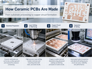
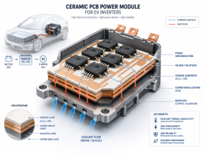
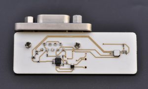
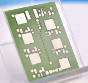
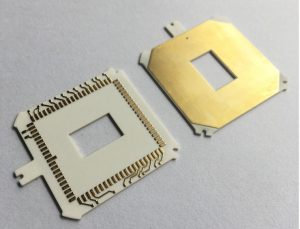
Ceramic PCBs are widely recognized for their thermal stability, outstanding insulation performance, and long-term reliability in demanding electronic applications. From automotive control systems to aerospace electronics and medical instruments, ceramic-based circuit boards are chosen when standard FR4 materials can no longer meet thermal or electrical requirements.
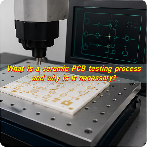
Testing is not simply a routine quality checkpoint. It is a carefully controlled verification system that confirms whether the board can survive electrical loads, thermal cycling, mechanical stress, and long operating hours without failure. In high-performance electronics, even a tiny defect in a ceramic substrate can influence signal transmission, solderability, or heat dissipation.
At EBest Circuit (Best Technology), ceramic PCB testing is integrated into every production stage, from incoming raw material inspection to final electrical verification. This approach helps ensure that each ceramic PCB prototype and production batch achieves consistent quality, dimensional precision, and dependable functionality for industrial applications.
What Is the Ceramic PCB Testing Process?
The ceramic PCB testing process refers to a series of inspections, measurements, and validation procedures performed before, during, and after production. Its purpose is to confirm that the ceramic PCB design matches technical specifications and can operate reliably under real application conditions.
Unlike ordinary printed circuit boards, ceramic PCBs use substrates such as aluminum oxide (Al2O3), aluminum nitride (AlN), or silicon nitride (Si3N4). These materials provide excellent thermal conductivity and electrical insulation, but they also require more specialized processing and inspection methods.
Testing usually begins long before manufacturing starts. Engineering teams first evaluate design files, Gerber data, drilling accuracy, copper layout, and thermal management structures. During production, additional inspections monitor ceramic surface quality, metallization consistency, dimensional tolerance, and layer alignment. After fabrication, the boards undergo electrical and reliability testing to verify performance.
The complete ceramic PCB manufacturing process typically includes testing stages such as:
- Raw material inspection
- Design verification
- Dimensional measurement
- Circuit continuity testing
- Insulation resistance testing
- Thermal shock testing
- Surface finish evaluation
- Solderability analysis
- Environmental reliability validation
Because ceramic materials behave differently from FR4 laminates, testing standards are often tighter. Small cracks, uneven metallization, or microscopic voids may influence long-term stability, especially in high-power applications.
For manufacturers like EBest Circuit (Best Technology), testing is not treated as a final step alone. It is a continuous quality management strategy integrated throughout the entire production workflow.
What Main Tests Are Included in Ceramic PCB Testing Process?
Ceramic PCB testing involves multiple inspection categories. Each test targets a different aspect of board reliability and electrical performance.
Visual and Microscopic Inspection
The first stage usually focuses on surface quality. Engineers inspect the board under magnification to identify:
- Surface scratches
- Ceramic cracks
- Metallization defects
- Copper contamination
- Misaligned drilling
- Uneven solder mask coverage
Since ceramic materials are rigid and brittle compared with traditional PCB materials, microscopic inspection becomes especially important.
Dimensional Accuracy Testing
Precision dimensions directly affect assembly compatibility. Automated optical measurement systems verify:
| Inspection Item | Purpose |
|---|---|
| Board thickness | Ensures thermal consistency |
| Hole diameter | Supports component fitting |
| Pad spacing | Prevents short circuits |
| Outline tolerance | Guarantees assembly alignment |
| Layer registration | Confirms multilayer accuracy |
Even slight dimensional deviations can influence mounting accuracy in high-density applications.
Electrical Testing
Electrical verification is one of the most critical parts of the ceramic PCB testing process. This stage confirms that conductive paths operate exactly as designed.
Common electrical tests include:
- Continuity testing
- Open/short circuit detection
- High-voltage insulation testing
- Dielectric strength testing
- Resistance measurement
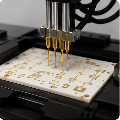
Flying probe systems and bed-of-nails fixtures are commonly used depending on production volume.
Thermal Reliability Testing
Ceramic PCBs are often selected for their superior thermal conductivity. Testing therefore focuses heavily on heat performance.
Typical thermal tests include:
- Thermal cycling
- Thermal shock exposure
- High-temperature storage
- Heat dissipation validation
- Power load simulation
These procedures help determine whether the board structure remains stable after repeated heating and cooling cycles.
Mechanical Strength Testing
Although ceramic substrates offer excellent rigidity, their brittleness requires careful evaluation. Mechanical tests may include:
- Flexural strength analysis
- Peel strength testing
- Shear testing
- Drop impact simulation
These tests help verify structural durability during assembly and operation.
Surface Finish Evaluation
Surface finishes directly influence soldering reliability and oxidation resistance. Inspection methods evaluate coating uniformity, thickness, and adhesion.
Popular surface finishes for ceramic PCBs include:
- ENIG (Electroless Nickel Immersion Gold)
- Silver plating
- Tin plating
- OSP coating
Each finish requires specific testing methods to verify quality consistency.
What Standards Are Followed in Ceramic PCB Testing?
The ceramic PCB industry follows strict international standards to maintain manufacturing consistency and reliability. These standards provide measurable benchmarks for inspection, electrical safety, thermal performance, and environmental durability.
Several major organizations define testing criteria for ceramic PCBs.
IPC Standards
IPC standards are widely adopted across the electronics industry. Important IPC specifications include:
| IPC Standard | Function |
|---|---|
| IPC-6012 | Qualification and performance of rigid PCBs |
| IPC-6013 | Flexible and rigid-flex PCB qualification |
| IPC-A-600 | Acceptability of printed boards |
| IPC-TM-650 | Standardized PCB test methods |
These standards help ensure that ceramic PCBs meet industry-accepted quality levels.
MIL Standards
Military electronics often require additional reliability testing due to harsh operating environments. MIL standards emphasize:
- Extreme temperature endurance
- Shock resistance
- Vibration durability
- Long operational lifespan
Many aerospace and defense applications rely on these advanced testing procedures.
ISO Quality Systems
Manufacturers operating under ISO9001 quality management systems maintain tighter production controls and traceability. At EBest Circuit (Best Technology), ISO-driven procedures help ensure stable manufacturing consistency across ceramic PCB production batches.
RoHS and REACH Compliance
Environmental compliance testing also plays a major role. Ceramic PCBs are often inspected for hazardous material restrictions under:
- RoHS directives
- REACH regulations
These certifications support global product compatibility and environmental responsibility.
Why Is Ceramic PCB Testing Important?
Testing protects product reliability, customer safety, and long-term operational stability. In many high-power electronic systems, board failure can cause expensive downtime or complete equipment malfunction.
Ceramic PCBs are commonly used in:
- Power electronics
- Automotive systems
- LED lighting
- RF communication
- Aerospace electronics
- Medical devices
In these applications, performance consistency matters tremendously.

Ensuring Thermal Reliability
One major reason for ceramic PCB popularity is heat management capability. Testing confirms whether thermal conductivity remains stable under real operating loads.
Without proper thermal verification, overheating can damage:
- Power semiconductors
- LED chips
- RF modules
- High-frequency circuits
Reliable testing helps prevent thermal failure before products reach the field.
Preventing Electrical Failures
Electrical testing detects hidden defects that may not appear during visual inspection. Tiny shorts, weak insulation areas, or incomplete conductive paths can create intermittent failures later.
This is especially critical in:
- High-voltage applications
- RF communication systems
- Medical monitoring equipment
Consistent testing greatly improves operational confidence.
Supporting Long-Term Product Stability
Ceramic materials are engineered for long service life. Reliability testing helps predict performance under extended operating conditions, including temperature fluctuations and humidity exposure.
Long-term testing also reduces warranty risks and improves customer satisfaction.
Improving Production Yield
Testing identifies process weaknesses early in production. Manufacturers can adjust parameters quickly before large-scale defects occur.
This helps improve:
- Manufacturing efficiency
- Product consistency
- Cost control
- Delivery stability
For ceramic PCB manufacturing, early defect detection can significantly reduce production waste.
How Does Ceramic PCB Design Affect Testing Results?
The ceramic PCB design stage directly influences testing performance and manufacturing success. A well-designed board is easier to fabricate, inspect, and validate.
Poor layout decisions can increase thermal stress, signal interference, or assembly challenges.
Trace Width and Spacing
Proper conductor spacing is critical for electrical reliability. Overly narrow spacing may increase short-circuit risk during manufacturing.
Design engineers carefully calculate:
- Current capacity
- Voltage clearance
- Signal integrity
- Thermal expansion effects
Accurate design improves both manufacturability and test pass rates.
Thermal Layout Optimization
Ceramic substrates are often selected for high thermal conductivity, especially aluminum nitride materials. Thermal simulation during ceramic PCB design helps engineers distribute heat efficiently.
Good thermal design improves:
- Component lifespan
- Temperature uniformity
- Power handling capability
Testing usually confirms whether these thermal objectives are achieved.
Via Structure Design
Via placement and metallization quality strongly affect electrical testing results. Improper via structures may create resistance instability or heat concentration areas.
Engineers often optimize:
| Design Element | Testing Influence |
|---|---|
| Via diameter | Current stability |
| Via density | Heat transfer |
| Pad size | Soldering reliability |
| Copper thickness | Resistance performance |
Thoughtful design reduces manufacturing complexity and improves reliability outcomes.
Layer Stackup Accuracy
Multilayer ceramic PCBs require extremely precise alignment. Any layer offset can affect impedance control or RF performance.
Testing validates whether the actual board matches the intended stackup configuration.
What Files Are Checked Before Ceramic PCB Production?
Before manufacturing begins, engineering teams carefully review customer files to minimize production risks and avoid dimensional inconsistencies.
This pre-production analysis is a highly important part of the ceramic PCB testing process.
Gerber File Review
Gerber files contain the complete circuit layout data for fabrication. Engineers verify:
- Copper layer accuracy
- Pad alignment
- Trace spacing
- Board outline dimensions
- Aperture consistency
Software tools help identify potential manufacturability issues before production starts.
Drill File Analysis
Drill files define hole positions and sizes. Accurate drilling is essential for multilayer alignment and component assembly.
Inspection focuses on:
- Hole diameter tolerance
- Hole-to-pad registration
- Mechanical clearance
For ceramic substrates, drilling precision becomes even more critical due to material hardness.
Stackup Verification
Engineers review stackup information to confirm:
- Layer sequence
- Ceramic material type
- Copper thickness
- Dielectric spacing
This stage helps ensure that the finished board can meet thermal and electrical requirements.
DFM Evaluation
Design for Manufacturability (DFM) analysis identifies production risks early. Manufacturers may recommend layout adjustments to improve:
- Yield rate
- Reliability
- Assembly compatibility
- Cost efficiency
At EBest Circuit (Best Technology), DFM verification is routinely integrated before ceramic PCB prototype production begins.
How Is a Ceramic PCB Prototype Tested?
A ceramic PCB prototype serves as an early validation stage before mass production. Prototype testing helps engineers confirm whether the design performs correctly in real-world conditions.
Compared with full-scale production, prototype testing is often more detailed and application-focused.
Functional Verification
Prototype boards are assembled and powered under controlled conditions. Engineers monitor:
- Signal transmission
- Voltage stability
- Thermal behavior
- Component interaction
This stage validates the overall ceramic PCB design concept.
Thermal Imaging Analysis
Infrared thermal cameras help visualize heat distribution across the board.
Thermal imaging can quickly reveal:
- Hotspots
- Uneven heat flow
- Insufficient thermal dissipation
- Overloaded components
This information is valuable for optimizing high-power applications.
Environmental Stress Testing
Prototype boards may undergo accelerated environmental simulations, including:
- High humidity exposure
- Temperature cycling
- Vibration testing
- Salt spray evaluation
These tests help predict long-term field performance.
Assembly Compatibility Testing
Engineers also verify whether the board integrates smoothly with:
- SMT assembly processes
- Reflow soldering profiles
- Housing structures
- Connectors and components
This reduces integration issues before full production begins.
How Are Ceramic PCB Circuits Electrically Tested?
Electrical testing ensures that every conductive path functions correctly and meets design specifications. Because ceramic PCBs are often used in high-frequency and high-power systems, electrical accuracy is especially important.
Flying Probe Testing
Flying probe systems use movable test probes to inspect circuits without requiring custom fixtures.
Advantages include:
- Flexible testing for prototypes
- Fast setup changes
- High accuracy for small batches
This method is commonly used during ceramic PCB prototype validation.
Bed-of-Nails Testing
For larger production volumes, bed-of-nails fixtures provide faster inspection speed.
This method simultaneously contacts multiple test points, improving production efficiency.
| Testing Method | Best Application |
|---|---|
| Flying probe | Prototype and low-volume runs |
| Bed-of-nails | Mass production |
| AOI inspection | Surface defect detection |
| X-ray inspection | Hidden structure analysis |
Insulation Resistance Testing
This procedure measures resistance between conductive paths to ensure proper electrical isolation.
High insulation resistance is critical for:
- High-voltage circuits
- RF modules
- Medical electronics
High-Potential Testing
High-potential (Hipot) testing applies elevated voltage to verify dielectric integrity.
This test helps identify:
- Weak insulation zones
- Material defects
- Potential leakage paths
Reliable Hipot performance demonstrates strong board insulation quality.
What Surface Finish Tests Are Used for Ceramic PCBs?
Surface finish quality strongly influences solderability, corrosion resistance, and assembly reliability.
Different finishes require different inspection methods during the ceramic PCB testing process.
Thickness Measurement
Coating thickness directly affects durability and soldering performance.
Testing methods may include:
- X-ray fluorescence analysis
- Microscopic cross-section inspection
- Chemical thickness measurement
Manufacturers carefully control plating uniformity to maintain stable assembly quality.
Solderability Testing
Solderability evaluation confirms whether components can bond properly to the board surface.
Testing usually simulates real soldering conditions under controlled temperatures.
Strong solderability helps improve:
- Joint reliability
- Assembly yield
- Long-term conductivity
Adhesion Testing
Adhesion tests evaluate how firmly the surface finish bonds to the ceramic substrate.
Poor adhesion may lead to peeling or cracking during thermal cycling.
Corrosion Resistance Testing
Environmental exposure testing helps verify oxidation resistance under humid or corrosive conditions.
This is especially valuable for:
- Automotive electronics
- Outdoor LED systems
- Industrial control equipment
Reliable surface finish performance contributes significantly to overall product lifespan.
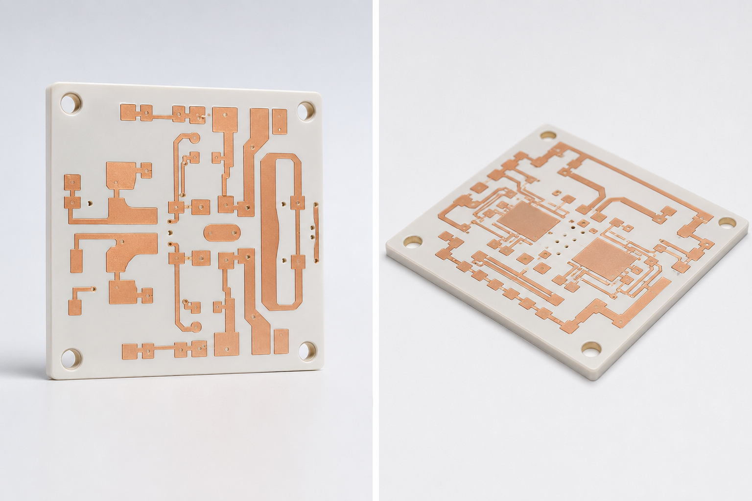
In today’s advanced electronics industry, the ceramic PCB testing process plays a central role in ensuring product reliability, thermal stability, and electrical accuracy. From design verification and raw material inspection to prototype validation and final electrical testing, every stage contributes to the long-term performance of ceramic PCBs.
At EBest Circuit (Best Technology), testing procedures are integrated throughout the complete ceramic PCB manufacturing process to maintain precision, reliability, and consistent quality standards for every project. Whether customers require a ceramic PCB prototype or full-volume production, comprehensive testing remains one of the most valuable safeguards for long-term electronic performance.
For more information about ceramic PCB manufacturing, ceramic PCB design, or prototype services, feel free to contact EBest Circuit (Best Technology) at sales@bestpcbs.com