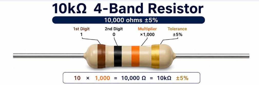
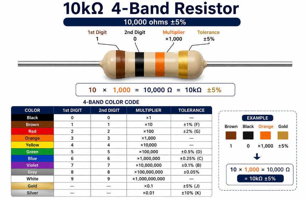
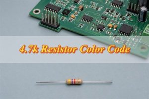
The standard 10k resistor color code is brown-black-orange for a 3-band value reading. A common 4-band 10k resistor is brown-black-orange-gold, meaning 10,000 ohms with ±5% tolerance.
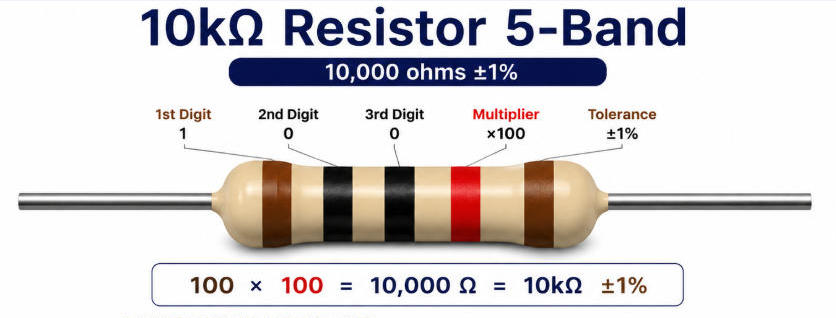
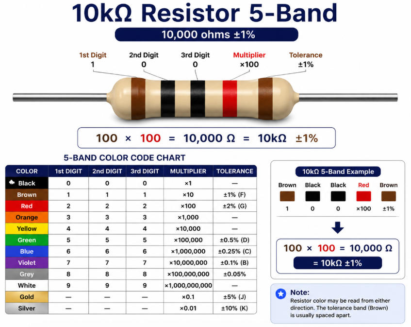
A common 5-band 10k resistor is brown-black-black-red-brown, meaning 10,000 ohms with ±1% tolerance.
A 10k resistor equals 10,000 ohms, or 10 kΩ. It is one of the most widely used resistor values in PCB circuits for pull-up, pull-down, voltage dividers, sensor inputs, timing networks, biasing circuits, and signal conditioning.
What Is a 10k Resistor?
A 10k resistor is a passive electronic component with a resistance value of 10,000 ohms. The letter k means kilo, so 10kΩ = 10 × 1,000Ω = 10,000Ω. In a circuit, a 10k resistor limits current, divides voltage, sets logic levels, or stabilizes input signals.
Why Is the 10k Resistor Color Code Important?
The 10k resistor color code is crucial to identify the resistor value before soldering, testing, repair, or replacement. Wrong resistor values can cause incorrect voltage levels, unstable sensor readings, MCU boot failure, weak pull-up signals, timing errors, or excessive current.
How Does a Resistor Color Code Work?
A resistor color code works by using colored bands to represent digits, multipliers, tolerance, and sometimes temperature coefficient.
Color
Digit
Multiplier
Common Tolerance
Black
0
×1
–
Brown
1
×10
±1%
Red
2
×100
±2%
Orange
3
×1,000
–
Yellow
4
×10,000
–
Green
5
×100,000
±0.5%
Blue
6
×1,000,000
±0.25%
Violet
7
×10,000,000
±0.1%
Gray
8
×100,000,000
±0.05%
White
9
×1,000,000,000
–
Gold
–
×0.1
±5%
Silver
–
×0.01
±10%
What Is the 4-Band 10k Resistor Color Code?
The 4-band 10k resistor color code is brown, black, orange, gold for a ±5% resistor. Calculation: 10 × 1,000 = 10,000Ω = 10kΩ.
What Is the 5-Band 10k Resistor Color Code?
The 5-band 10k resistor color code is brown, black, black, red, brown for ±1% precision. Calculation: 100 × 100 = 10,000Ω = 10kΩ.
10k Resistor Color Bands Compared: 4-Band vs 5-Band
Type
Color Bands
Value
Tolerance
Best Use
4-band
Brown-black-orange-gold
10kΩ
±5%
General pull-up, pull-down, LED signal circuits
5-band
Brown-black-black-red-brown
10kΩ
±1%
Precision sensor, reference voltage, industrial control
6-band
Value bands + tolerance + TCR band
10kΩ
Depends
Temperature-sensitive circuits
How to Read a 10k Resistor Color Code Correctly?
Place the tolerance band on the right, read left to right. For brown-black-orange-gold, brown=1, black=0, orange=×1,000, gold=±5%, resulting in 10kΩ ±5%.
What Is the 10k Surface Mount Resistor Code?
Common SMD markings: 103 (10+3 zeros = 10kΩ) or 1002 (100+2 zeros = 10kΩ).
Materials, Features, and Advantages
10k resistors may be carbon film, metal film, thick film SMD, thin film SMD, or wirewound. Features: 10kΩ value, ±5% or ±1% tolerance, through-hole or SMD packages, moderate power rating, widely applicable.
Applications in PCB Design
Used for pull-up/pull-down circuits, voltage dividers, sensor interfaces, timing, transistor bias, communication line biasing, and general PCB logic stabilization.
Procurement and Manufacturing Tips
Check BOM, package, tolerance, power rating, and source reliability. Use AOI and electrical testing in mass production. Confirm resistor value to avoid wrong placements or rework.
Testing and Quality Standards
Verify with multimeter, LCR meter, flying probe, or functional testing. Factory quality standards include component inspection, IPC workmanship, solder joint inspection, and traceability.
Common Failures and How to Avoid Them
Failures include wrong value, cracked body, poor solder, overheating, color misreading. Avoid by BOM confirmation, correct reel loading, process verification, and first-article inspection.
FAQs About 10k Resistor Color Code
What is the 10k ohm resistor color code? Brown-black-orange for 3-band; brown-black-orange-gold for 4-band ±5%.
What is the 4 band 10k resistor color code? Brown, black, orange, gold; 10 × 1,000 = 10kΩ ±5%.
What is the 5 band 10k resistor color code? Brown, black, black, red, brown; 100 × 100 = 10kΩ ±1%.
What does brown black orange gold resistor mean? 10kΩ ±5%, standard 4-band through-hole resistor.
What are the 10k resistor colors? Brown, black, orange for value; gold for ±5% tolerance; 5-band: brown-black-black-red-brown.
How do you read a 10k resistor color code? Place tolerance band right, read left-to-right, convert colors to digits, apply multiplier.
What is the 10k surface mount resistor code? 103 or 1002 markings; 10kΩ SMD resistor.
Is a 103 resistor the same as a 10k resistor? Yes, 103 = 10kΩ.
What is a 10k linear potentiometer pinout? Three pins: two ends of resistive track, middle wiper; wiper output changes as shaft rotates.
Can I replace a 10k resistor with another value? Only after circuit verification; different values may alter voltage, bias, timing.
Conclusion
The 10k resistor color code varies with 4-band or 5-band type: 4-band is brown-black-orange-gold, 5-band is brown-black-black-red-brown. SMD markings include 103 or 1002. For precision applications, choose appropriate tolerance and material type.
If you need keywords-related products or services, EBest PCB can support PCB manufacturing, PCB assembly, OEM production, ODM development, sample builds, batch production, and custom engineering solutions.
If you’re sourcing reliable PCB/PCBA manufacturing — OEM, ODM, prototyping, mass production, or custom engineering solutions — reach out to our engineering team for technical support and a quote at sales@bestpcbs.com.
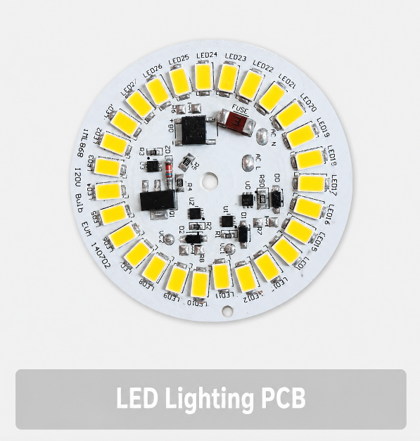
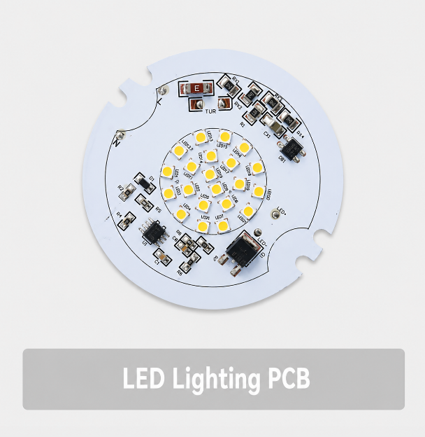
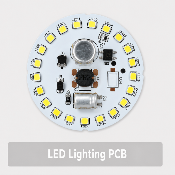
LED Lighting PCB provides electrical connection, mechanical support, and heat dissipation for LED modules. EBest Circuit manufactures custom LED Lighting PCB using aluminum PCB, FR4 PCB, and turnkey assembly services for residential, commercial, high-power, automotive, and outdoor lighting projects.
Are you worried about these problems in LED Lighting PCB projects?
Delivery delays: Unstable production cycles, slow sample approval, material shortages, or batch delays may disrupt your project schedule.
Hidden costs: Extra charges may appear after quotation approval, including tooling changes, material upgrades, testing fees, or assembly adjustments.
Quality instability: Batch variation may cause flickering, overheating, soldering defects, color inconsistency, or field failure risks.
As a 20+ years PCB manufacturer, EBest Circuit provides manufacturing and assembly solutions for global lighting brands, OEM factories, and engineering projects.
Delivery predictability: ERP + MES production tracking supports 7-day standard delivery, 48-hour urgent response, and delay rate controlled at ≤2%.
Cost transparency: BOM-level cost modeling locks pricing before production and covers material, fabrication, assembly, testing, packaging, and export documentation.
Quality reliability: AOI inspection, flying probe testing, thermal validation, and functional testing support 100% critical process inspection, ≤0.3% defect rate, and ≥98% batch consistency.
Welcome to contact us if you have any request for LED lighting PCB manufacturing and assembly: sales@bestpcbs.com.
What Is an LED Lighting PCB?
An LED lighting PCB is a printed circuit board used to mount, connect, and power LED components in lighting products. It provides current paths, mechanical support, thermal transfer, and assembly stability for LED modules.
Unlike standard circuit boards, LED lighting boards must handle heat, current load, brightness stability, and long operating hours. Poor PCB quality may cause hot spots, unstable light output, solder joint fatigue, and early LED failure.
EBest Circuit manufactures custom LED PCB, aluminum PCB, FR4 PCB, and assembled LED modules for residential, commercial, industrial, automotive, and outdoor lighting applications.
Why Do LED Lighting Products Need Reliable PCB Solutions?
LED lighting products rely on stable PCB performance because heat, current, and soldering quality directly affect lifespan. A weak PCB may reduce brightness, increase failure rates, and raise after-sales cost.
Reliable PCB solutions help control:
Thermal stability: Better heat transfer reduces LED junction temperature.
Electrical safety: Stable copper design supports consistent current flow.
Assembly yield: Accurate pads and solder mask control reduce SMT defects.
Long-term reliability: Better materials reduce delamination, oxidation, and early failure.
Choosing the right manufacturer affects warranty risk, brand reputation, and total project cost.
What LED Lighting PCB Types Can We Manufacture?
EBest Circuit manufactures LED lighting boards according to power level, heat dissipation demand, product structure, and assembly requirements. Instead of using one fixed PCB type, we help customers choose the right structure for actual working conditions.
Common PCB types include:
Aluminum LED PCB: Suitable for high-power LED modules, street lights, flood lights, panel lights, and outdoor lighting products.
FR4 LED PCB: Suitable for low-power and medium-power residential lighting, commercial lighting, control circuits, and cost-sensitive products.
Metal Core PCB: Designed for products that require stronger thermal performance, stable mechanical support, and long operating life.
Heavy Copper LED PCB: Used for products with higher current load, stronger power demand, or long continuous operation.
High TG LED PCB: Suitable for lighting products exposed to higher working temperature or repeated thermal stress.
Multilayer LED PCB: Used when modules include driver circuits, control functions, sensors, communication modules, or compact routing.
Flexible and Rigid-Flex LED PCB: Suitable for curved lighting structures, automotive lighting, wearable lighting, compact modules, and special installation spaces.
The right type should match LED power, thermal path, fixture housing, installation environment, and production cost.
Aluminum PCB vs FR4 PCB for LED Lighting
Aluminum PCB and FR4 PCB solve different lighting problems. The choice affects heat dissipation, electrical stability, product cost, assembly yield, and long-term reliability.
Item
Aluminum PCB
FR4 PCB
Thermal Conductivity
1.0–3.0 W/m·K
0.3–0.5 W/m·K
Copper Thickness
1oz–3oz
1oz–2oz
Best Use
High-power LED
Low to medium-power LED
Heat Control
Strong
Limited
Cost
Higher
Lower
Applications
Street light, flood light, panel light
Indoor lamp, control PCB, low-power module
Aluminum PCB is better for high-power LED lighting because it transfers heat away from LED components more efficiently. This helps reduce hot spots, solder joint stress, brightness decay, and early failure.
FR4 PCB is better for low-power LED lighting where heat is easier to control. It is often used in indoor lamps, control boards, small LED modules, and commercial lighting products where cost control matters more than extreme thermal performance.
From a project cost view, aluminum PCB is usually more expensive because the material and processing requirements are higher. However, for street lights, flood lights, grow lights, and high-power modules, better heat dissipation can reduce field failure and after-sales cost.
FR4 PCB is practical when the LED current is lower, the fixture has a separate heat sink, or the board mainly supports control functions. It can reduce material cost, simplify production, and support multilayer routing more easily.
In short, choose aluminum PCB for high-heat lighting products and choose FR4 PCB for low-power or cost-sensitive lighting applications.
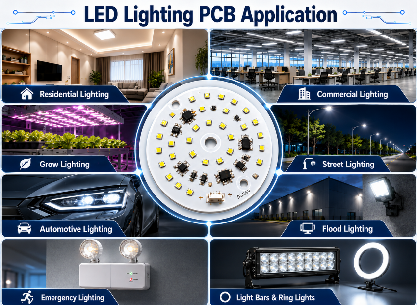
LED Lighting PCB Applications We Support
LED lighting boards are used in many lighting products, and each application has different priorities. Outdoor lighting focuses on heat, waterproof structure, and long service life. Indoor lighting focuses on cost, shape, brightness consistency, and assembly efficiency.
EBest Circuit supports PCB for:
Residential lighting: Ceiling lights, downlights, panel lights, and indoor lamps.
Street lighting: High-power street light modules and aluminum PCB solutions.
Flood lighting: High-brightness PCB for outdoor and industrial lighting.
Grow lighting: Stable current and heat control for horticultural lighting.
Automotive lighting: Vehicle lamps, signal lights, and interior lighting.
Emergency lighting: Backup lighting systems and emergency light circuit boards.
Light bars and ring lights: Custom-shaped boards for compact lighting products.
For each application, we match material, copper thickness, LED layout, and assembly process to the final product structure.
How Do We Improve Heat Dissipation for LED PCB?
Heat dissipation directly affects brightness stability, color consistency, solder joint life, and product lifespan. If heat is not controlled, LEDs may suffer brightness drop, color shift, solder fatigue, and early failure.
Aluminum substrate selection: Aluminum PCB improves heat transfer for high-power LED modules.
Copper thickness optimization: 1oz, 2oz, or thicker copper supports current flow and heat spreading.
Thermal pad control: Proper LED pad design improves heat transfer from LED packages.
LED spacing optimization: Correct spacing reduces local hot spots and uneven heating.
Surface finish control: HASL and ENIG are selected based on soldering and reliability needs.
Thermal testing: Temperature rise is checked during sample validation and production testing.
For high-power projects, aluminum PCB, suitable copper thickness, and fixture-level thermal review are recommended before mass production.
What LED Lighting PCB Assembly Services Do We Provide?
EBest Circuit provides assembly services from bare PCB fabrication to finished LED modules. This helps customers reduce supplier coordination, shorten project cycles, and control quality from one source.
Assembly services include:
SMT assembly: For 2835, 5730, 3030, 5050, COB-related components, and LED driver parts.
Through-hole assembly: For connectors, terminals, switches, and power components.
Mixed assembly: For boards with both SMD and through-hole components.
Functional testing: Voltage, current, brightness, polarity, and continuity checks.
Turnkey service: PCB fabrication, component sourcing, assembly, testing, and packaging.
This service supports lighting brands, product developers, and OEM lighting manufacturers.
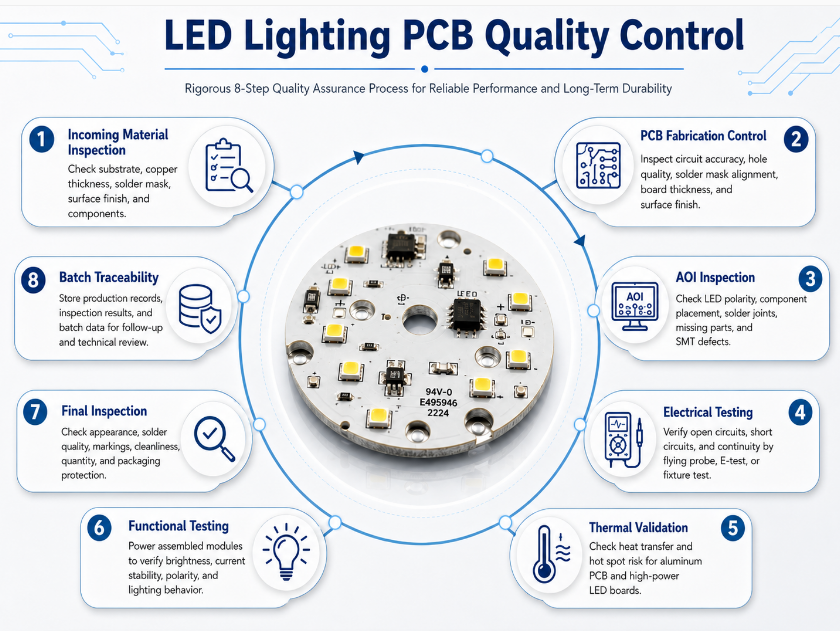
How Do We Control LED Lighting PCB Quality?
EBest Circuit controls quality from material inspection to final function testing. Each step reduces overheating, soldering defects, electrical failure, and batch inconsistency.
Incoming material inspection: We check substrate, copper thickness, solder mask, surface finish, and components before production.
PCB fabrication control: We inspect circuit accuracy, hole quality, solder mask alignment, board thickness, and surface finish.
AOI inspection: Automated optical inspection checks LED polarity, component placement, solder joints, missing parts, and visible SMT defects.
Electrical testing: Flying probe testing, E-test, or fixture testing checks open circuits, short circuits, and continuity.
Thermal validation: Aluminum PCB and high-power LED boards are checked for heat transfer and hot spot risk.
Functional testing: Assembled modules are powered under working voltage to verify brightness, current stability, polarity, and lighting behavior.
Final inspection: Board appearance, solder quality, markings, cleanliness, quantity, and packaging protection are checked before shipment.
Batch traceability: Production records, inspection results, and batch data are stored for follow-up and technical review.
How Can We Help Optimize LED Light PCB Cost?
Cost optimization is not about choosing the cheapest board. It is about reducing unnecessary cost while keeping thermal performance, electrical stability, assembly yield, and long-term reliability under control.
Best Technology helps optimize cost through early engineering review, material selection, BOM checking, and production planning.
Choose the right material: Use aluminum PCB for high-heat products and FR4 PCB for low-power indoor lighting to avoid over-specification.
Optimize copper thickness: Select suitable copper weight based on current load and heat spreading. Too much copper increases cost, while too little copper increases heat risk.
Improve PCB size and panel utilization: Review board outline, spacing, and panel layout to reduce material waste and improve production efficiency.
Review LED layout before production: Proper spacing reduces hot spots, improves light uniformity, and avoids redesign after sampling.
Control BOM cost: Review LEDs, resistors, connectors, drivers, and other parts to find stable, cost-effective alternatives.
Reduce assembly defects: DFM review helps avoid solder bridging, wrong pad size, poor polarity marking, and SMT rework.
Verify prototype before mass production: Sample testing confirms thermal performance, brightness, current stability, and assembly quality.
Optimize order quantity: Proper batch planning reduces setup cost, material waste, packaging cost, and shipping cost per unit.
The final goal is stable LED performance, predictable delivery, and reliable mass production at a controlled total cost.
Case Study: High-Power LED Street Light PCB Project
Project Background A European lighting customer was developing a high-power LED street light for city roads and industrial areas. Their previous supplier had unstable delivery, uneven batch quality, and poor heat dissipation, causing fixture assembly delays and higher project risk.
Project Requirements
Quantity: 5,000 high-power LED boards for outdoor street lighting.
Power: Support LED modules above 100W.
Material: Use aluminum PCB or high thermal conductivity material.
Quality: Control defect rate at ≤0.3% and batch consistency at ≥98%.
PCB structure optimization: Use 2oz aluminum PCB for better current capacity and heat spreading.
LED layout improvement: Adjust LED spacing and copper distribution to reduce hot spots and improve light uniformity.
Thermal management: Use high thermal conductivity aluminum substrate and optimized thermal paths.
Assembly control: Apply AOI inspection, electrical testing, thermal validation, and functional testing during production.
Delivery management: Use ERP + MES tracking to control schedule and reduce delivery uncertainty.
Project Results
On-time delivery: All 5,000 pieces were completed and shipped on schedule.
Stable thermal performance: Hot spot temperature was controlled below 45°C under defined test conditions.
Consistent quality: Batch consistency reached ≥98%, and defect rate was controlled at ≤0.3%.
Customer approval: The customer approved mass production and continued cooperation on related street light and flood light projects.
This project shows how Best Technology helps customers solve delivery, heat dissipation, and batch quality problems through proper material selection, production control, and full-process testing.
Why Choose EBest as Your LED Lighting PCB Manufacturer?
EBest Circuit, also known as Best Technology, is a China source PCB manufacturer with 20+ years of experience. We provide one-stop solutions from design support, prototype, and mass production to component sourcing, assembly, testing, and global delivery.
Experienced manufacturer: 20+ years of PCB manufacturing experience reduces production risk.
One-stop service: Design support, prototype, mass production, sourcing, assembly, and testing are handled by one supplier.
Diverse PCB options: FR4, aluminum, metal core, heavy copper, high TG, multilayer, and impedance control PCB are available.
Strong production capacity: Monthly capability reaches 260,000 sq. ft / 28,900 sq. m, with 1,000+ boards completed monthly.
Fast delivery: Expedited boards can be shipped within 24 hours when project conditions allow.
Certified quality: IATF 16949, ISO 9001:2015, ISO 13485:2016, AS9100D, REACH, RoHS, and UL are supported.
Global supply: China source factory supply with worldwide shipping and export documentation.
Cost transparency: BOM-level cost planning helps lock total project cost before production.
Reliable quality: Critical processes are inspected, with defect rate controlled at ≤0.3% and batch consistency reaching ≥98%.
Custom project support: OEM and ODM services support residential, commercial, automotive, street light, flood light, grow light, and emergency lighting projects.
FAQs About LED Lighting PCB
Q1: What copper thickness is common for LED lighting PCB? A1: Common copper thickness includes 1oz, 2oz, and 3oz. For high-power modules, 2oz copper is often used to improve current capacity and heat spreading.
Q2: What thermal conductivity is suitable for aluminum PCB? A2: Common aluminum PCB thermal conductivity is 1.0–3.0 W/m·K. Higher thermal conductivity is better for high-power lighting with stronger heat output.
Q3: Can LED PCB be custom-shaped? A3: Yes. Boards can be made in round, ring, bar, square, panel, or irregular shapes according to fixture structure and mounting requirements.
Q4: What surface finishes are common? A4: HASL and ENIG are common. ENIG provides flatter pads and better solderability, especially for higher-reliability assembly projects.
Q5: Can you assemble 2835 and 5730 LEDs? A5: Yes. We support 2835, 5730, 3030, 5050, and other standard SMD LED packages based on BOM and placement files.
Q6: What files are needed for quotation? A6: Recommended files include Gerber, BOM, pick-and-place file, quantity, material, copper thickness, surface finish, and testing requirements.
Q7: How can I reduce LED PCB cost? A7: Cost can be reduced by optimizing panel usage, material selection, copper thickness, BOM, DFM, and order quantity before production.
Q8: What causes LED PCB overheating? A8: Common causes include poor thermal path, thin copper, dense LED spacing, weak substrate, or insufficient fixture-level cooling.
Q9: Do you provide prototypes? A9: Yes. Prototypes help verify thermal performance, electrical stability, LED layout, brightness behavior, and assembly quality before mass production.
Q10: What is the typical lead time? A10: Standard PCB orders can be completed in about 7 working days. Assembly lead time depends on BOM availability, quantity, and testing requirements.
Q11: Do you support outdoor LED projects? A11: Yes. We support street lights, flood lights, grow lights, emergency lights, and other outdoor lighting products.
Q12: Can one order include aluminum and FR4 PCB? A12: Yes. One project can include aluminum PCB for LED power modules and FR4 PCB for control circuits.
Q13: What defect rate is achievable? A13: Under defined quality criteria, defect rate can be controlled at ≤0.3%, with batch consistency reaching ≥98%.
Q14: Do you provide global delivery? A14: Yes. We support worldwide delivery by air, sea, or express, based on project urgency and order volume.
Q15: Can you review LED PCB design before production? A15: Yes. We can review Gerber files, copper width, thermal path, panelization, pad design, and assembly risks before production.
Request a Quote for Your LED Lighting PCB Project
LED lighting PCB performance depends on material selection, heat dissipation, copper design, solder quality, and batch control. Aluminum PCB is suitable for high-power lighting, while FR4 PCB is practical for cost-sensitive indoor lighting.
For procurement, buyers should evaluate delivery stability, quality traceability, testing capability, material selection, and total project cost, not only unit price. EBest Circuit offers custom manufacturing, assembly, cost review, quality inspection, and global delivery from China.
Send your Gerber files, BOM, quantity, material requirement, and assembly details to sales@bestpcbs.com for a fast LED lighting PCB quotation.
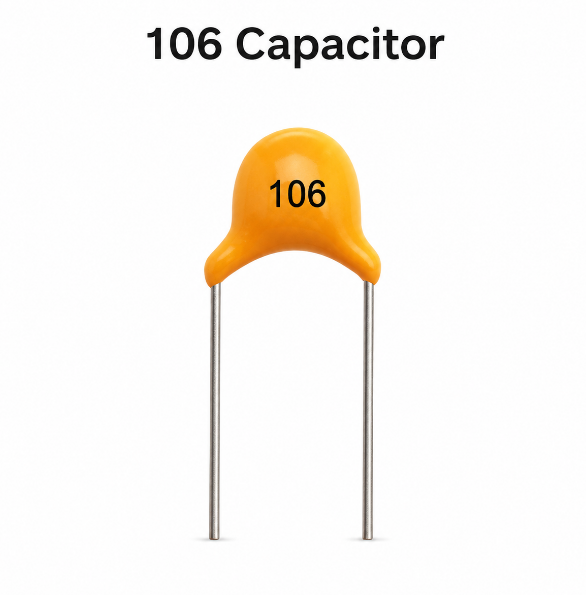
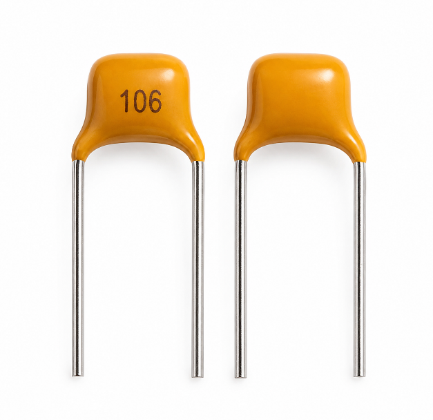
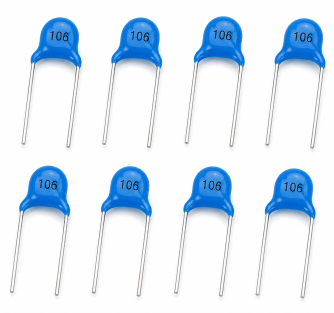
A 106 capacitor has a capacitance value of 10 uF, which equals 10,000 nF or 10,000,000 pF. The number “106” follows the standard three-digit capacitor code rule: the first two digits are the base number, and the third digit shows how many zeros are added in picofarads.
This guide explains the 106 capacitor value, capacitor code 106, voltage rating, tolerance, polarity, package size, datasheet parameters, testing method and replacement rules. It also adds practical PCB assembly advice, so the capacitor can be selected, mounted and tested correctly in real electronic products.
What Does 106 Mean on a Capacitor?
A 106 capacitor means the capacitor has a value of 10 uF. In the standard capacitor marking system, “10” is the significant number, and “6” means six zeros are added after it in picofarads.
The calculation is 10 × 10⁶ pF = 10,000,000 pF. After unit conversion, this becomes 10,000 nF or 10 uF. This is why a capacitor marked 106 is not 106 pF, but a much larger 10 uF capacitor.
The 106 marking appears on ceramic capacitors, tantalum capacitors, electrolytic capacitors and SMD capacitors. However, this marking only identifies capacitance. Voltage rating, tolerance, polarity, dielectric material and package size must be checked separately before replacement or PCB assembly.
What Is the Value of a 106 Capacitor in uF, nF and pF?
The value of a 106 capacitor is 10 uF, equal to 10,000 nF and 10,000,000 pF. This conversion is the first thing to confirm when reading capacitor code 106 on a PCB or component body.
Code
uF
nF
pF
106
10 uF
10,000 nF
10,000,000 pF
A 10 uF capacitor is commonly used for power decoupling, voltage smoothing, noise filtering and local energy storage. In power rails, it helps reduce voltage drops when ICs, modules or sensors suddenly draw current.
However, capacitance alone does not decide final performance. A 106 ceramic capacitor, 106 tantalum capacitor and 106 electrolytic capacitor can behave differently because ESR, leakage current, polarity, temperature performance and voltage derating are different.
How to Read a 106 Capacitor Code?
A 106 capacitor code is read by using the first two digits as the base number and the third digit as the multiplier in picofarads. For 106, the value is 10 × 1,000,000 pF, which equals 10 uF.
If a letter appears after 106, it may show tolerance, voltage code, dielectric series or manufacturer-specific information. The meaning depends on capacitor type, so the datasheet should be checked when the marking is not fully clear.
Marking
Common Meaning
106
10 uF capacitance
106J
10 uF, often ±5% tolerance
106K
10 uF, often ±10% tolerance
106M
10 uF, often ±20% tolerance
106C
10 uF, may indicate a voltage code on some SMD tantalum capacitors
106E
10 uF, may indicate a voltage code on some SMD tantalum capacitors
For PCB assembly, never approve a component only by the printed code. The full manufacturer part number should be used in the BOM to avoid wrong voltage, wrong package or wrong capacitor type.
Difference Between 105, 106 and 107 Capacitor
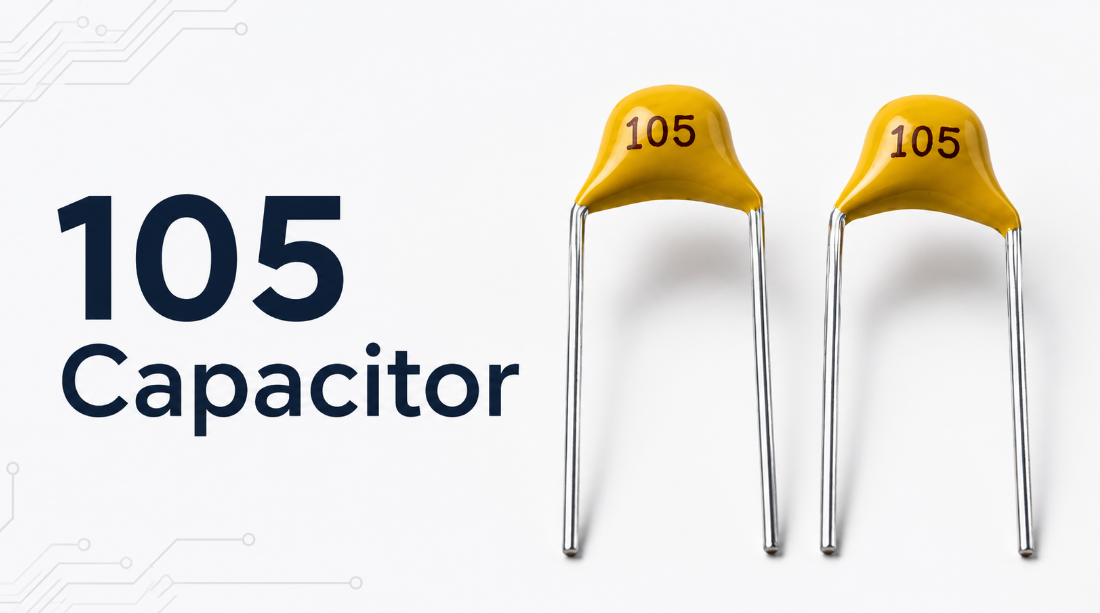
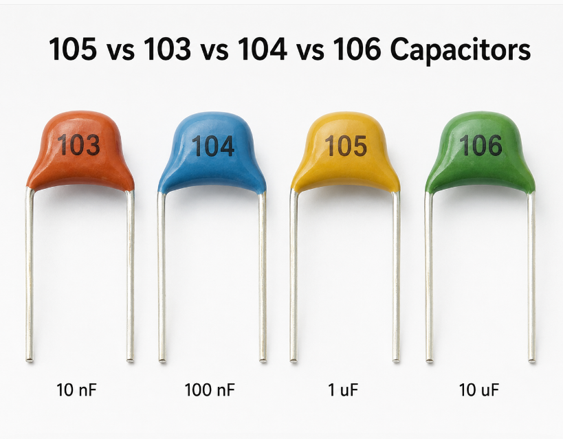
The difference between 105, 106 and 107 capacitors is capacitance value. 105 = 1 uF, 106 = 10 uF, and 107 = 100 uF.
Code
Value
Conversion
Common Use
105
1 uF
1,000 nF
Small decoupling, timing, signal coupling
106
10 uF
10,000 nF
Power filtering, module decoupling, voltage smoothing
107
100 uF
100,000 nF
Bulk filtering, power input smoothing, energy storage
Each code increases by 10 times. A 105 capacitor has lower energy storage than a 106 capacitor, while a 107 capacitor has much higher capacitance and may change startup current, charging time and PCB space.
In repairs, replacing 106 with 105 can reduce filtering capacity and cause ripple or reset problems. Replacing 106 with 107 may work in some power circuits, but it may also affect regulator stability, inrush current and cost.
What Types of 106 Capacitors Are Common?
Common 106 capacitors include ceramic, tantalum, aluminum electrolytic and SMD capacitors. They all provide 10 uF capacitance, but their electrical performance, polarity and assembly risks are different.
Ceramic type: low ESR, compact size, good for high-frequency decoupling near ICs.
Tantalum type: stable capacitance, compact package, usually polarized and sensitive to surge.
Electrolytic type: cost-effective for bulk filtering, usually larger and polarized.
SMD type: suitable for automated SMT PCB assembly and compact electronic products.
Through-hole type: used where manual assembly, mechanical strength or repairability matters.
For high-density PCB assembly, ceramic and SMD tantalum 106 capacitors are common. For power input filtering or low-cost products, electrolytic capacitors may be selected when board space allows.
Does a 106 Capacitor Have Polarity?
A 106 capacitor may or may not have polarity. Ceramic 106 capacitors are usually non-polarized, while tantalum and electrolytic 106 capacitors are usually polarized.
Non-polarized ceramic capacitors can be mounted in either direction. Polarized capacitors must be installed with the correct positive and negative orientation. Reverse installation can cause leakage current, overheating, short circuit, swelling or complete capacitor failure.
This is especially important in PCB assembly. Many SMD tantalum capacitors mark the positive terminal with a stripe, while many aluminum electrolytic capacitors mark the negative terminal with a stripe. Because marking rules are not always the same, the datasheet, PCB silkscreen and assembly drawing should be checked before production.
What Voltage Is a 106 Capacitor?
A 106 capacitor does not have one fixed voltage. The code 106 only identifies capacitance, while voltage rating depends on the actual capacitor series, package, dielectric material and manufacturer part number.
Marking
Capacitance
Voltage
106 6.3V
10 uF
6.3V
106 10V
10 uF
10V
106 16V
10 uF
16V
106 25V
10 uF
25V
106 35V
10 uF
35V
106 50V
10 uF
50V
For stable circuit operation, the voltage rating should be higher than the actual working voltage. In many PCB designs, a practical rule is to choose a capacitor with enough derating margin, especially when ripple, voltage spikes, high temperature or long service life are involved.
For example, a 10 uF 16V capacitor may be acceptable on a 5V rail, while a 10 uF 6.3V capacitor may be risky if the rail has spikes or poor transient control.
What Is the Tolerance of a 106 Capacitor?
The tolerance of a 106 capacitor depends on the tolerance letter and component type. Common tolerance codes include J = ±5%, K = ±10% and M = ±20%.
Marking
Value
Tolerance
Normal Range
106J
10 uF
±5%
9.5 uF–10.5 uF
106K
10 uF
±10%
9 uF–11 uF
106M
10 uF
±20%
8 uF–12 uF
Tolerance affects the real capacitance value under standard test conditions. For power decoupling, ±10% or ±20% may be acceptable in many circuits. For timing, filtering, sensing or analog applications, tighter tolerance can improve circuit consistency.
Ceramic capacitors may also lose effective capacitance under DC bias. Therefore, a 10 uF ceramic capacitor may measure lower in actual operation, especially in small packages or higher-voltage circuits.
What Size Is a 106 Capacitor?
The size of a 106 capacitor depends on capacitor type, voltage rating, dielectric material, package code and temperature grade. A 10 uF low-voltage SMD ceramic capacitor may be small, while a 10 uF high-voltage electrolytic capacitor may be much larger.
Type
Common Size
SMD ceramic capacitor
0402, 0603, 0805, 1206
SMD tantalum capacitor
A, B, C, D, E case
Aluminum electrolytic capacitor
4 mm to 8 mm diameter or larger
Through-hole ceramic capacitor
varies by voltage and lead spacing
Higher voltage ratings usually require larger packages. Higher reliability grades, wider temperature ranges and lower ESR versions may also increase size and cost.
In PCB assembly, the selected capacitor must match the land pattern, height limit, polarity mark, pick-and-place capability and reflow soldering process. A wrong size can cause mounting failure, solder bridging, tombstoning or mechanical interference.
106 Capacitor Datasheet Overview
A 106 capacitor datasheet should be reviewed before replacement, purchasing or PCB assembly. The marking 106 confirms 10 uF, but the datasheet confirms whether the part can work safely in the target circuit.
Parameter
Typical Information
Capacitance
10 uF
Voltage rating
6.3V, 10V, 16V, 25V, 35V, 50V
Tolerance
±5%, ±10%, ±20%
Temperature range
-55°C to +85°C or +125°C
ESR
type and series dependent
Leakage current
material and voltage dependent
Package
SMD, radial, axial, case code
Polarity
polarized or non-polarized
Dielectric
X5R, X7R, tantalum, aluminum electrolytic
Compliance
RoHS, REACH, halogen-free options
For mass production, the datasheet also helps confirm soldering profile, storage condition, MSL level, shelf life, reel packaging, ripple current and reliability rating.
A complete BOM should include the manufacturer part number, value, voltage, tolerance, package, dielectric type and approved alternatives. This reduces purchasing mistakes and improves PCB assembly yield.
Where Is a 106 Capacitor Commonly Used?
A 106 capacitor is commonly used for power filtering, decoupling, voltage stabilization, ripple reduction and short-term energy storage. Its 10 uF value is large enough for many local power rails while still available in compact packages.
MCU power rails: reduces voltage drops and random reset problems.
Wireless modules: supports current peaks in Wi-Fi, Bluetooth, GPS and IoT devices.
Power supplies: smooths ripple and improves transient response.
Sensor circuits: stabilizes analog and digital supply lines.
LED drivers: helps reduce flicker and supply fluctuation.
Automotive electronics: supports stable operation under vibration and temperature change.
Industrial control PCB: improves noise immunity and long-term reliability.
In PCB layout, a 106 capacitor is often placed near IC power pins, regulators, connectors, sensors and communication modules. Short traces and good grounding improve its filtering effect.
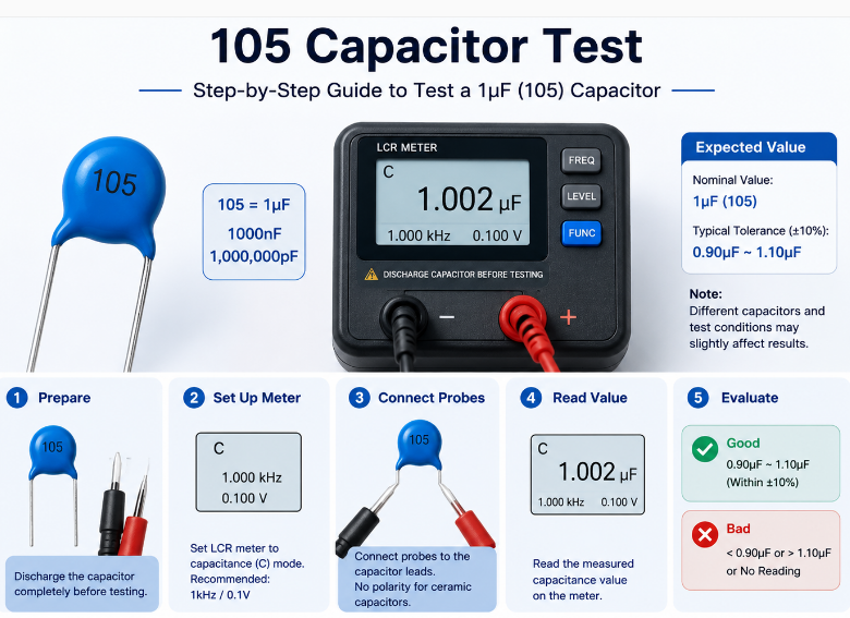
How to Test a 106 Capacitor with a Multimeter?
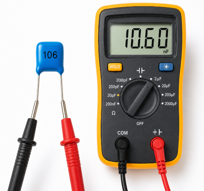
To test a 106 capacitor with a multimeter, first confirm that the circuit is powered off and the capacitor is safely discharged. A 106 capacitor should normally measure close to 10 uF, but the acceptable range depends on its tolerance.
Turn off the power first Disconnect the device from the power source before testing. Testing a charged capacitor may damage the multimeter or cause unsafe discharge.
Discharge the capacitor safely Use a suitable resistor to discharge the capacitor before measurement. Do not short the terminals directly, especially for larger capacitors or power supply circuits.
Check whether it is still on the PCB If the capacitor remains soldered on the PCB, nearby components may affect the reading. For a more accurate result, remove one terminal or test the capacitor after desoldering it.
Set the multimeter to capacitance mode Select the capacitance function on the multimeter. Then connect the probes to the capacitor terminals. For polarized 106 capacitors, keep the probe direction correct if required by the meter.
Compare the measured value with 10 uF A normal 106 capacitor should read close to 10 uF. For example, a 106K capacitor has ±10% tolerance, so a reading between 9 uF and 11 uF is usually acceptable.
Watch for abnormal readings If the reading is 0 uF, extremely low, unstable, or overloaded, the capacitor may be shorted, open, aged, cracked or damaged.
Check ESR when capacitance looks normal Some failed capacitors still show normal capacitance but have high ESR. In power circuits, high ESR can cause ripple, startup failure, voltage drop or unstable operation.
Inspect the capacitor body Look for cracks, bulging, leakage, burn marks or broken terminals. Physical damage is often a clear sign that the capacitor should be replaced.
For PCB repair and production testing, capacitance measurement is only the first check. If the capacitor is used in a power rail, ESR, leakage current, polarity and circuit waveform should also be reviewed.
How to Replace a 106 Capacitor?
To replace a 106 capacitor, do not choose a new part only by the “106” marking. The replacement must match 10 uF capacitance, voltage rating, tolerance, polarity, package size, capacitor type and circuit requirement.
Match the capacitance value A 106 capacitor equals 10 uF. The replacement should normally keep the same capacitance unless the circuit design allows a different value.
Choose the same or higher voltage rating The replacement voltage should be equal to or higher than the original part. For example, a 10 uF 25V capacitor can often replace a 10 uF 16V capacitor if the size and type match.
Do not reduce the voltage rating casually Replacing a 25V capacitor with a 16V capacitor may reduce reliability, especially in circuits with ripple, voltage spikes or high temperature.
Check polarity before soldering Ceramic 106 capacitors are usually non-polarized, but tantalum and electrolytic 106 capacitors are usually polarized. Reverse mounting can cause leakage, overheating or failure.
Match the package size and footprint The new capacitor must fit the PCB pad, height limit and assembly process. A wrong package may cause soldering defects, poor contact or mechanical interference.
Confirm the capacitor type A 106 ceramic capacitor, 106 tantalum capacitor and 106 electrolytic capacitor may all be 10 uF, but their ESR, leakage current, polarity and stability are different.
Check ESR requirements Some voltage regulators require a specific ESR range for stable output. Replacing tantalum with ceramic or electrolytic without checking ESR may cause oscillation or unstable voltage.
Review temperature and reliability grade For industrial, automotive or outdoor PCB applications, choose parts with suitable temperature ratings such as -40°C to +105°C or -55°C to +125°C.
Use the full manufacturer part number For PCB assembly, the BOM should include the full part number, voltage, tolerance, package, dielectric and approved alternatives. Listing only “106 capacitor” can cause purchasing mistakes.
Test the board after replacement After soldering, check polarity, solder joints, capacitance and power rail behavior. Then run functional testing to confirm that the circuit starts and operates normally.
In PCB assembly, a correct replacement should not only match the 106 capacitor value. It should also support the circuit’s voltage, temperature, ESR, layout, sourcing and long-term reliability requirements.
How to Choose the Right 106 Capacitor for PCB Assembly?
Choose the right 106 capacitor by matching circuit performance, assembly process, reliability target and sourcing stability. The best capacitor is the one that works reliably after soldering, testing and long-term operation.
Confirm circuit function: use ceramic for local decoupling, tantalum for stable compact filtering, and electrolytic for bulk smoothing.
Check voltage margin: select a voltage rating higher than the actual rail voltage to reduce failure risk.
Review tolerance: choose tighter tolerance for timing, analog and sensitive filtering circuits.
Match package: confirm footprint, height, polarity and pick-and-place compatibility.
Check ESR: regulator output capacitors may require a specific ESR range for stability.
Consider temperature: use wider temperature grades for industrial, automotive and outdoor products.
Control sourcing: list full manufacturer part numbers and approved alternates in the BOM.
Verify production quality: use AOI, polarity inspection, ICT and functional testing to catch assembly defects.
For turnkey PCB assembly, the 106 capacitor should be checked during BOM review, incoming inspection and first-article testing. This prevents wrong-value mounting, reverse polarity, soldering defects and field reliability problems.
FAQs About 106 Capacitor
Q1: Is a 106 capacitor always 10 uF? A1: Yes. In the standard three-digit capacitor code, 106 means 10 uF. It also equals 10,000 nF and 10,000,000 pF. However, the number 106 does not show voltage, tolerance, polarity or package size.
Q2: Is a 106 capacitor the same as a 106 pF capacitor? A2: No. A 106 capacitor is not 106 pF. The third digit is a multiplier, so 106 means 10 × 10⁶ pF, which equals 10 uF. This is one of the most common capacitor code reading mistakes.
Q3: What does 106K mean on a capacitor? A3: 106K usually means 10 uF with ±10% tolerance. Under standard test conditions, the measured capacitance may be around 9 uF to 11 uF. For purchasing or PCB assembly, the datasheet should still be checked.
Q4: What does 106J mean on a capacitor? A4: 106J usually means 10 uF with ±5% tolerance. This tolerance is tighter than 106K and can be useful in circuits where capacitance accuracy affects timing, filtering or analog signal behavior.
Q5: What does 106C capacitor mean? A5: A 106C capacitor usually means 10 uF, while “C” may be a voltage code or series code on some SMD tantalum capacitors. Since marking systems vary, confirm the exact voltage and case size from the datasheet.
Q6: What does 106E capacitor mean? A6: A 106E capacitor usually indicates 10 uF, while “E” may represent a voltage code in some capacitor marking systems. It should not be treated as a universal rule because different manufacturers may use different coding methods.
Q7: Can I replace a 106 16K capacitor with a 106 25K capacitor? A7: Usually yes, if the package, polarity, ESR and temperature rating match. Both are 10 uF ±10%, while 25V has a higher voltage rating than 16V. The main concern is whether the new capacitor fits the PCB footprint.
Q8: Can I replace a 106 25K capacitor with a 106 16K capacitor? A8: Only if the circuit voltage is safely below 16V with enough margin. If the original capacitor was 25V, using 16V may reduce reliability under voltage spikes, ripple or high temperature. For production, avoid lowering voltage without approval.
Q9: Why does my 106 ceramic capacitor measure less than 10 uF? A9: Ceramic capacitors, especially MLCC types, can lose effective capacitance under DC bias. A marked 10 uF capacitor may show a lower value in real operation, especially when the package is small or the applied voltage is high.
Q10: Does a 106 capacitor have positive and negative terminals? A10: It depends on the capacitor type. Ceramic 106 capacitors are usually non-polarized, while tantalum and electrolytic 106 capacitors are usually polarized. For polarized capacitors, wrong orientation can cause overheating, leakage or failure.
Q11: What happens if a 106 capacitor is installed backwards? A11: If the capacitor is polarized, reverse installation can cause serious failure. The capacitor may heat up, leak, short circuit or fail during power-on testing. This is a major risk for 106 tantalum capacitors and 106 electrolytic capacitors.
Q12: Which is better, 106 ceramic capacitor or 106 tantalum capacitor? A12: A 106 ceramic capacitor is better for low ESR and high-frequency decoupling. A 106 tantalum capacitor may provide more stable capacitance in compact power rails. The better choice depends on voltage, ESR, polarity, ripple and reliability requirements.
Q13: Can a wrong 106 capacitor cause PCB failure? A13: Yes. A wrong 106 capacitor can cause unstable voltage, ripple, regulator oscillation, startup failure, repeated resets or wireless module dropouts. During PCB testing, engineers should check value, voltage, ESR, polarity, soldering and waveform behavior.
Q14: What should buyers check before ordering 106 capacitors? A14: Buyers should check 10 uF value, voltage rating, tolerance, package, polarity, dielectric type, manufacturer part number, compliance and lifecycle status. For PCB assembly, the BOM should never list only “106 capacitor.”
Q15: Is a 106 capacitor suitable for industrial PCB assembly? A15: Yes, if the part matches the working environment. Industrial PCB projects often require higher voltage margin, wide temperature range, stable sourcing, strong soldering control and strict inspection for long-term reliability.
Conclusion
A 106 capacitor has a value of 10 uF, equal to 10,000 nF or 10,000,000 pF. The code 106 only confirms capacitance, while voltage rating, tolerance, polarity, package size, material type, ESR and temperature range must be checked separately. For PCB projects, the right choice should match circuit voltage, filtering purpose, assembly footprint, reliability target and approved sourcing requirements.
EBest Circuit is a China source factory and global PCB assembly manufacturer. We support BOM review, component sourcing, custom PCB assembly, quality inspection and bulk production for electronic projects using 106 capacitors and related components. Send your BOM, Gerber files and project requirements to sales@bestpcbs.com for a fast quotation and practical assembly support.
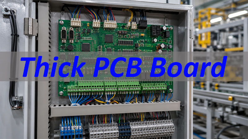
Thick PCB board is a printed circuit board designed with a greater board thickness than common standard PCB designs for stronger structure, multilayer routing, connector stability, and special product requirements. This article explains how EBest Circuit (Best Technology), branded as EBEST, supports thick PCB board projects through stack-up review, drilling control, plating review, thickness tolerance control, testing, and shipment documentation.
What problems do buyers often face when sourcing a thick PCB board?
Unclear thickness requirement: The buyer knows the final thickness but not the stack-up.
Drilling risk: Small holes on thick boards may be difficult to plate reliably.
Wrong copper assumption: Thick board does not always mean thick copper PCB board.
Impedance uncertainty: Multilayer PCB board thickness can affect impedance results.
Weak documentation: Missing test reports or inspection standards can delay approval.
EBEST helps reduce these risks through engineering-led manufacturing review.
Stack-up review: We check layer structure, dielectric thickness, copper weight, and final thickness.
Drilling review: We review finished hole size, aspect ratio, hole tolerance, and plating risk.
Copper review: We separate PCB board thickness from PCB board copper thickness.
Impedance review: We check impedance notes together with stack-up and material data.
Shipment control: We can provide COC, microsection, test, solderability, and copper thickness reports when required.
EBest Circuit (Best Technology) is a PCB and PCBA manufacturer supporting FR4 PCB, high-Tg FR4 PCB, thick PCB board, multilayer PCB, HDI PCB, heavy copper PCB, aluminum PCB, copper base PCB, ceramic PCB, RF microwave high-frequency PCB, rigid-flex PCB, and PCBA assembly. Our standard PCB capabilities include 1–50 layers, FR4 Tg 130–180 materials, standard board thickness from 0.4 mm to 6.0 mm, FR4 inner copper from 0.5 oz to 6 oz, FR4 outer copper from 0.5 oz to 10 oz, controlled impedance, ENIG, ENEPIG, HASL, OSP, immersion tin, immersion silver, hard gold, soft gold, carbon ink, and gold finger plating. For thick PCB board quotes, please send Gerber files, stack-up, material notes, copper thickness, finished board thickness, hole size, impedance requirements, surface finish, testing requirements, quantity, and delivery target to sales@bestpcbs.com.
What Should Buyers Confirm Before Quoting a Thick PCB Board?
A thick PCB board quote should start with the real structure, not only the final board thickness. EBEST reviews the design first so the quotation can reflect manufacturability, testing, and delivery risk.
Before asking for a thick PCB board quote, buyers should confirm:
Final board thickness: Such as 2.0 mm, 2.4 mm, 3.2 mm, 4.8 mm, or custom thickness.
Layer count: Thick boards are often multilayer PCB projects.
Material: FR4, high-Tg FR4, ISO370HR, Rogers, ceramic, metal base, or specified laminate.
Copper weight: Inner and outer copper must be checked layer by layer.
Impedance: Stack-up and trace geometry must match impedance notes.
Reports: COC, microsection, test, solderability, and copper thickness reports may be required.
A quote based only on board size and quantity is not enough for thick PCB board manufacturing.
The correct starting point is a complete stack-up, finished thickness target, drilling requirement, copper structure, and test standard.
How Does EBEST Review PCB Board Thickness Before Production?
EBEST reviews PCB board thickness before production because thickness affects pressing, drilling, plating, routing, V-CUT, connectors, and assembly fit. A thick board needs more than a simple “final thickness” number.
Our review usually covers:
Finished PCB board thickness
PCB board thickness tolerance
Layer count and stack-up
Core and prepreg structure
Copper distribution
Hole size after plating
Aspect ratio
Impedance notes
Edge clearance and routing process
Panelization and tooling holes
EBEST supports standard board thickness from 0.4 mm to 6.0 mm, while special thickness projects can be reviewed separately. For most PCB projects, thickness tolerance is commonly controlled around ±10% unless the drawing gives a stricter requirement.
For a thick PCB board, the final thickness should match both product fit and manufacturing reality.
If the thickness target is clear but the stack-up is not clear, EBEST will review the structure before confirming production.
When Does Standard PCB Board Thickness Become a Thick PCB Board?
Standard PCB board thickness is often around 1.6 mm, but a board becomes a thick PCB board when the final thickness creates extra manufacturing or assembly concerns. The exact boundary depends on layer count, material, hole size, copper weight, and product use.
A simple way to understand it:
0.8 mm–1.6 mm: Common standard PCB board thickness.
2.0 mm–3.2 mm: Often treated as a thicker board for structural or connector needs.
Above 3.2 mm: Usually needs closer review for drilling, plating, and routing.
Above 4.0 mm: Often requires stricter hole, aspect ratio, and process review.
This is not only about thickness in millimeters. A 2.4 mm 12-layer board may be more complex than a 3.0 mm 2-layer board.
Buyers should not only ask, “How thick are PCB boards?” They should ask, “Can this PCB board thickness be manufactured with my hole size, copper, impedance, and test requirements?”
That question leads to a more useful engineering review.
Why Do Thick PCB Boards Need Careful Drilling and Plating Review?
Thick PCB boards need careful drilling and plating review because holes become harder to process as board thickness increases. The thicker the board, the more important aspect ratio and hole copper become.
Key risks include:
Small holes on thick boards: Higher aspect ratio increases plating difficulty.
Insufficient hole copper: Weak plating can affect reliability.
Finished hole tolerance: Drawings usually show plated finished hole size.
Burrs and sharp edges: Thick boards need careful routing and deburring.
Solder mask in holes: Some projects require no solder mask inside plated holes.
Tooling needs: Panel tooling holes and optical fiducials may be required.
For plated through holes, EBEST reviews finished hole size, board thickness, drilling capability, and copper plating requirement together. If a customer requires 1.5 mil hole copper with a minimum of 1 mil, that requirement must be confirmed before production.
The drilling process decides whether the thick PCB board can be manufactured reliably.
The plating process decides whether the board can survive real electrical and mechanical use.
How Are PCB Board Thickness and Copper Thickness Different?
PCB board thickness and PCB board copper thickness are different specifications. Board thickness means the total finished PCB thickness, while copper thickness means the copper weight or copper thickness on each layer.
This difference matters because a thick PCB board is not always a thick copper PCB board.
For example:
A 2.4 mm FR4 PCB with 1 oz copper is a thick board, but not a heavy copper board.
A 1.6 mm PCB with 6 oz copper is a heavy copper PCB board, but not necessarily a thick board.
A multilayer thick PCB board may use mixed copper weights across different layers.
Buyers should confirm both:
PCB board thickness: Final mechanical thickness.
PCB board copper thickness: Copper weight on each layer.
EBEST reviews board thickness and copper thickness separately because they affect different manufacturing risks.
Board thickness affects drilling, routing, assembly fit, and connector matching. Copper thickness affects etching, current capacity, spacing, plating, and cost.
What Manufacturing Risks Should Thick PCB Board Buyers Watch For?
Thick PCB board buyers should watch for risks that are easy to miss during quotation. These risks often appear later in drilling, plating, impedance, testing, or final inspection.
Common risks include:
Unverified stack-up: Final thickness cannot be controlled without layer structure.
High aspect ratio: Thick boards with small holes need stronger drilling review.
Hole copper risk: Plated holes must meet reliability and inspection requirements.
Wrong test level: Some projects require 100% continuity testing before shipment.
Sharp edges or burrs: Thick boards need clean final routing and edge finishing.
Missing shipment reports: Some customers need COC, microsection, test, solderability, and copper reports.
EBEST can review thick PCB board projects under IPC-6012 Type 3 Class 3 requirements when required by customer drawings. We can also support 100% electrical continuity testing, flying probe test requirements, microsection reports, solderability reports, copper thickness reports, and shipment documentation.
For thick PCB board projects, the safest approach is to review manufacturing risk before production.
This is faster than solving quality problems after delivery.
Thick PCB Board Case: How Did EBEST Support a Multilayer Industrial Control Project?
A customer needed a custom thick PCB board for a multilayer industrial control project. The board required a controlled stack-up, impedance review, stable plated holes, strict testing, and shipment reports before delivery.
This was a 12-layer FR4 PCB using ISO370HR material, with a finished board thickness of 2.286 mm ±10%, ENIG surface finish, green solder mask, white silkscreen, and controlled impedance requirements based on the customer’s PDF stack-up and impedance notes.
EBEST reviewed the project around manufacturing reliability, not only board thickness.
Key support points included:
Stack-up review: EBEST checked the 12-layer structure, ISO370HR material, copper distribution, and final thickness target.
Impedance review: The impedance requirement was reviewed according to the customer’s PDF structure and impedance notes.
Drilling and plating control: The project required plated hole copper of 1.5 mil, with a minimum of 1 mil.
Testing control: All boards required 100% continuity testing before shipment, with flying probe test voltage at 250V.
Shipment documentation: EBEST prepared shipment support based on required reports, including COC, microsection, test, solderability, and copper thickness reports.
Important project parameters:
Application: Multilayer industrial control PCB
PCB type: 12-layer FR4 PCB
Material: ISO370HR
Finished thickness: 2.286 mm ±10%
Surface finish: ENIG, Au 1 μin
Solder mask / silkscreen: Green solder mask, white silkscreen
Impedance: Controlled impedance required
Hole copper: 1.5 mil target, 1 mil minimum
Test requirement: 100% continuity test, flying probe test at 250V
Standard: IPC-6012, Type 3, Class 3
Reports: COC, microsection, test, solderability, and copper thickness reports
This case shows why thick PCB board manufacturing must start with stack-up engineering support. The customer did not only need a thick board; they needed a board that could meet thickness, impedance, hole copper, test, marking, and shipment requirements.
FAQs About Thick PCB Board
What Is a Thick PCB Board? A thick PCB board is a PCB with greater finished thickness than common standard boards, often used for stronger structure, multilayer routing, connector stability, or special product requirements.
How Thick Is a Standard PCB Board? A common standard PCB board thickness is around 1.6 mm, but actual thickness can vary by product, stack-up, material, and customer requirement.
What Is the Maximum Thickness of PCB Board EBEST Can Review? EBEST supports standard board thickness from 0.4 mm to 6.0 mm, and special thick PCB board projects can be reviewed based on stack-up, material, hole size, copper weight, and process requirements.
Is a Thick PCB Board the Same as a Thick Copper PCB Board? No. A thick PCB board refers to final board thickness, while a thick copper PCB board refers to copper weight or copper thickness.
Why Is Stack-Up Important for Thick PCB Boards? Stack-up affects finished thickness, impedance, copper distribution, drilling, plating, press-fit parts, and final reliability.
What Files Should I Send for a Thick PCB Board Quote? Please send Gerber files, stack-up, material notes, copper thickness by layer, finished board thickness, hole size, impedance requirements, surface finish, testing requirements, reports required, quantity, and delivery target.
To conclude, thick PCB board is used when a PCB needs greater mechanical thickness, multilayer routing, connector stability, controlled impedance, or special manufacturing requirements. This article explained how buyers should confirm thickness, stack-up, drilling, plating, copper thickness, impedance, testing, and reports before ordering.
EBest Circuit (Best Technology) supports thick PCB board projects with stack-up engineering support, FR4 and high-Tg material review, multilayer PCB manufacturing, drilling and plating review, controlled impedance, ENIG, ENEPIG, 100% electrical testing when required, and shipment documentation. For your custom thick PCB board project, please send your files and requirements to sales@bestpcbs.com.
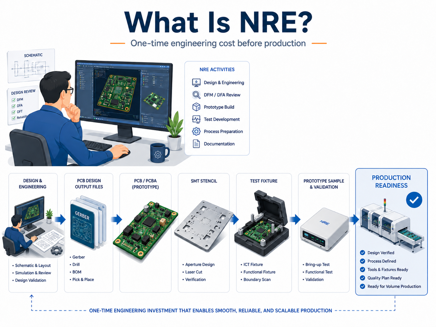
NRE stands for Non-Recurring Engineering, a one-time cost used to prepare a custom product, PCB, PCBA, mechanical part, or electronic device for stable production. This guide explains what NRE includes, why it matters, how it is calculated, how buyers can reduce unnecessary cost, and how to evaluate NRE charges before placing an OEM or ODM order.
For many buyers, NRE is confusing because it appears before mass production starts. It may include stencil fees, tooling, fixture design, test program development, engineering validation, documentation, prototyping, or process setup. The key point is simple: NRE is not a hidden fee when it is clearly explained. It is the engineering work that turns a design file into a manufacturable product.
What Is NRE?
NRE, or Non-Recurring Engineering, refers to the one-time engineering cost required to design, develop, test, validate, or prepare a product before regular production begins. It is different from unit cost because it does not repeat with every production run.
In electronics manufacturing, NRE may cover PCB production setup, SMT stencil creation, fixture design, programming, DFM review, test jig development, sample validation, tooling, firmware support, or production documentation. In mechanical manufacturing, it may include molds, CNC fixtures, die tooling, or custom process development.
A simple way to understand it:
Cost Type
Meaning
Example
NRE cost
One-time project setup cost
Tooling, stencil, fixture, engineering validation
Unit cost
Repeated product cost
PCB, components, assembly labor, packaging
Testing cost
May be one-time or recurring
Test jig development is NRE; each test operation may be recurring
Certification cost
Usually project-specific
CE, UL, RoHS-related documentation or third-party testing
NRE is common in custom manufacturing because every new product needs preparation before it can be built consistently.
Why Is NRE Important?
NRE is important because it decides whether a product can move from design to production with fewer risks. A low unit price is not useful if the design has poor manufacturability, unstable yield, weak testing, or unclear documentation.
For PCB and PCBA projects, NRE often supports:
Better DFM and DFA review
More stable sample builds
Correct solder paste stencil design
Accurate ICT, FCT, or programming fixtures
Better process repeatability
Lower rework risk
Faster transition from prototype to batch production
NRE also improves cost visibility. Instead of hiding engineering work inside the unit price, many manufacturers separate it so the buyer can see what is being charged and why.
In serious OEM and ODM production, NRE should be treated as an investment in production readiness, not just an extra fee.
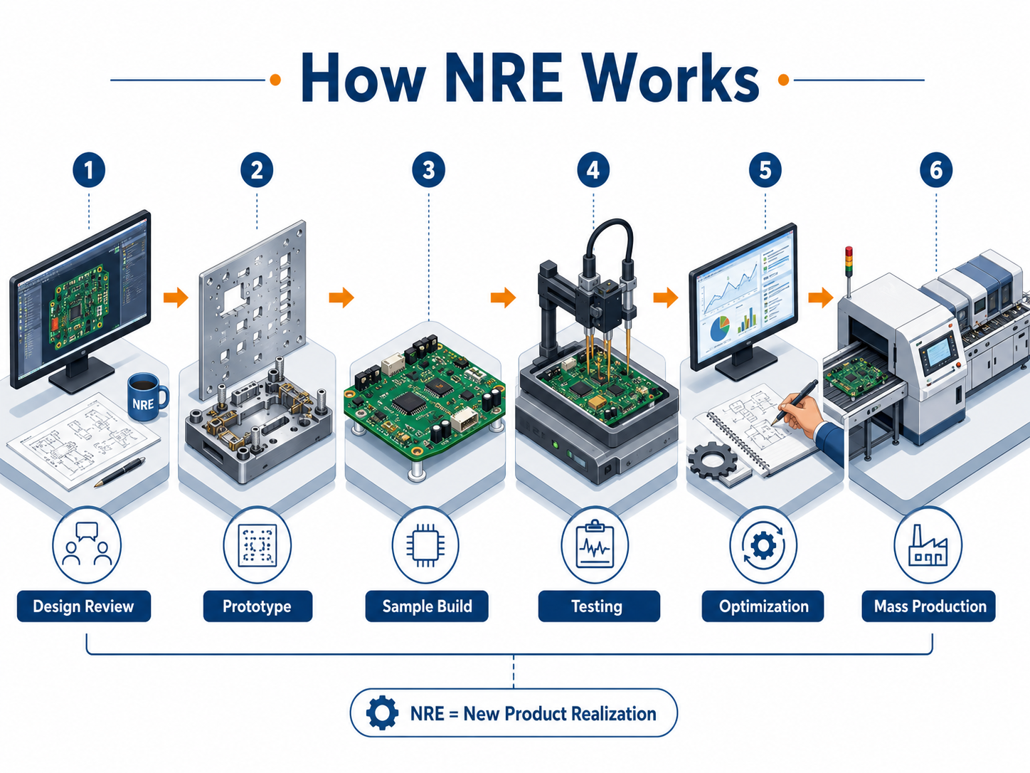
How Does NRE Work in a Manufacturing Project?
NRE usually appears at the beginning of a project. The manufacturer reviews the files, checks the production requirements, estimates the engineering workload, and provides a quotation.
Once the NRE work is completed, the same tooling, fixture, stencil, or engineering file can usually be reused for later batches of the same product version.
However, if the product design changes, extra NRE may be required. For example, changing the PCB layout, component package, enclosure, connector position, or firmware interface may require new tooling or test development.
What Does NRE Usually Include?
NRE may include different items depending on the product type and manufacturing process. In electronics manufacturing, the most common items are engineering review, production setup, tooling, test development, and documentation.
NRE Item
Common Use
Typical Reason
PCB production setup
Bare board fabrication
CAM review, film/tooling data, panelization
SMT stencil
PCBA assembly
Solder paste printing for surface-mount parts
Test fixture
ICT/FCT testing
Stable electrical or functional test
Programming fixture
MCU, IC, memory programming
Batch programming efficiency
Assembly fixture
Mechanical or box-build assembly
Positioning, alignment, repeatability
Tooling
Custom shape, housing, metal part, plastic part
Production preparation
DFM/DFA review
PCB, PCBA, mechanical design
Reduce manufacturing risk
Process engineering
Custom process setup
Improve yield and consistency
Documentation
Work instructions, inspection plan, test report format
Production control
What Is the Difference Between NRE and Unit Cost?
NRE is paid once for project preparation. Unit cost is paid for every product manufactured.
For example, if a PCBA project requires a 600 USD test fixture and the order quantity is 100 pieces, the NRE impact is 6 USD per board if divided across the first batch. If the total production volume reaches 10,000 pieces, the same fixture cost becomes only 0.06 USD per board.
This is why NRE looks expensive in prototype orders but becomes reasonable in mass production.
Item
NRE Cost
Unit Cost
Payment pattern
One-time
Repeated
Related to quantity
Indirectly
Directly
Main purpose
Prepare production
Build each product
Example
Fixture, stencil, tooling
PCB, components, assembly
Best evaluated by
Total project value
Per-piece price
For buyers, the right question is not only “Can you remove the NRE?” A better question is “What does this NRE cover, and can it reduce my later production risk?”
What Types of NRE Are Used in Electronics Manufacturing?
In electronics manufacturing, NRE can be divided into several practical categories. Each category supports a different part of production readiness.
Type of NRE
Description
Example
Engineering NRE
Design review, process planning, technical adjustment
DFM report, stack-up review
Tooling NRE
Physical tooling used for production
SMT stencil, carrier, fixture
Testing NRE
Equipment or software for inspection and validation
ICT jig, FCT fixture
Programming NRE
Software or hardware setup for chip programming
MCU flashing fixture
Documentation NRE
Controlled files for repeatable production
Work instruction, QC checklist
Certification-related NRE
Support for compliance preparation
Material declarations, test support
For PCB assembly, stencil and fixture fees are the most common. For box-build and electromechanical products, assembly fixtures and functional test systems become more important.
What Materials and Tools Are Involved in NRE?
NRE is not only an engineering service. It may also include physical materials, tooling parts, and dedicated equipment.
Common examples include stainless steel SMT stencils, aluminum or FR4 carriers, acrylic inspection fixtures, pogo pin test jigs, CNC-machined positioning tools, plastic injection molds, die-casting molds, cable harness boards, customized trays, programming adapters, and production gauges.
For PCB and PCBA projects, a test fixture may include:
Pogo pins
Fixture plate
Wiring harness
Control board
Connector interface
Pneumatic or manual press structure
Test software or firmware interface
Labeling and traceability setup
The more complex the test requirement, the higher the NRE may be. A simple continuity test fixture costs far less than a full functional test system with power loading, signal simulation, firmware communication, and automatic pass/fail judgment.
What Are the Key Features of NRE?
NRE has several features that buyers should understand before approving a quotation.
Feature
Meaning for Buyers
One-time nature
Usually paid once for one product version
Project-specific
Cannot normally be reused for another customer’s product
Design-sensitive
Major design changes may create new NRE
Volume-dependent impact
Higher production volume reduces per-unit impact
Quality-related
Good NRE can reduce failure, rework, and unstable yield
Documentation-driven
Clear scope prevents disputes
The most important feature is project specificity. A custom fixture, stencil, or test program is usually built for one product. It cannot be used freely on another design.
This is why NRE should be linked to clear files, revision numbers, tooling scope, and production requirements.
What Are the Advantages of Paying NRE?
NRE can feel uncomfortable at the quotation stage, especially for buyers comparing multiple suppliers. However, when used correctly, it brings clear value.
Main advantages include:
More reliable first article production
Lower hidden engineering risk
Faster ramp-up to mass production
Better inspection coverage
More stable product quality
Clearer production documentation
Easier repeat orders
Lower long-term failure cost
In PCBA manufacturing, a properly designed functional test fixture can detect wrong components, solder defects, reversed polarity, open circuits, firmware errors, and abnormal current before the product ships. That single NRE item may prevent expensive field failures later.
For high-reliability applications such as industrial control, medical electronics, automotive electronics, aerospace-related equipment, and power electronics, NRE is often necessary for process control.
What Are the Limitations of NRE?
NRE also has limitations. It does not automatically guarantee perfect production. It only creates the engineering foundation for better production control.
Common limitations include:
It may increase early project cost
It may not be refundable after tooling starts
It may need to be updated after design revision
It may not cover third-party certification unless clearly stated
It may not include unlimited engineering changes
It may not reduce unit cost in very small orders
For low-volume prototypes, buyers should control NRE carefully. A simple engineering sample may not need an expensive fixture. But for a product that will move into batch production, skipping all NRE may create higher cost later.
How Is NRE Calculated?
NRE is usually calculated based on engineering time, tooling material, fixture complexity, test coverage, process difficulty, and project risk.
Key cost factors include:
Cost Factor
Impact on NRE
Product complexity
More parts, layers, interfaces, or tolerances increase engineering work
Design maturity
Unstable files create more review and revision work
Tooling requirement
Custom tooling increases upfront cost
Test requirement
ICT, FCT, burn-in, or calibration increases fixture cost
Production volume
Higher volume may justify better tooling
Quality class
Industrial, medical, automotive, or aerospace projects need tighter control
Documentation
More reports and traceability increase engineering workload
Certification support
Compliance-related preparation may add cost
For electronics projects, NRE should be itemized whenever possible. Buyers should ask for a breakdown instead of accepting a single unclear line.
A clear NRE quote may show stencil cost, test fixture cost, programming fixture cost, engineering setup cost, and documentation cost separately.
How Can Buyers Reduce NRE Cost?
NRE cost can often be reduced through better preparation, clearer files, and smarter project planning. The goal is not to remove every NRE item. The goal is to avoid repeated, unnecessary, or poorly defined NRE.
Practical ways to reduce NRE include:
Provide complete Gerber, BOM, CPL, schematic, drawings, and test requirements
Confirm design revision before tooling starts
Use standard components and common packages where possible
Avoid unnecessary mechanical complexity
Ask whether the stencil or fixture can be reused for later batches
Separate prototype-stage NRE from mass-production-stage NRE
Confirm whether the supplier can absorb small setup fees for larger orders
Use modular test fixtures when suitable
Review DFM feedback before sample production
Lock key specifications before ordering tooling
For PCBA projects, an incomplete BOM is a common reason for extra engineering time. Missing MPNs, unclear substitutes, wrong footprints, and unconfirmed polarity markings can all increase setup work.
How Should NRE Be Compared Between Suppliers?
Comparing NRE only by price can be misleading. A lower NRE quote may exclude important items, while a higher NRE quote may include fixtures, documentation, and validation that another supplier charges later.
A better comparison method is shown below:
Comparison Point
What to Ask
Scope
What exactly does the NRE include?
Ownership
Who owns the tooling or fixture after payment?
Reuse
Can it be reused for repeat orders?
Revision rule
What happens if the design changes?
Testing coverage
What failures can the fixture detect?
Documentation
Will test reports or work instructions be provided?
Lead time
How long does tooling or fixture development take?
Refund rule
Is any part refundable if the project stops?
Maintenance
Who maintains or replaces worn tooling?
A reliable supplier should be able to explain NRE in plain language. If the explanation is vague, the buyer should ask for clarification before approving the order.
How Do You Choose the Right NRE Strategy?
The right NRE strategy depends on the project stage, order quantity, product complexity, and quality requirement.
For early prototypes, keep NRE lean. Focus on design validation, basic stencil, manual testing, and DFM feedback.
For pilot runs, add stronger process control. This may include dedicated fixtures, inspection plans, programming methods, and early functional testing.
For mass production, invest in stable tooling, automated or semi-automated testing, controlled documentation, traceability, and quality records.
A practical rule: do not overinvest before the design is stable, but do not underinvest before mass production.
What Industries Commonly Use NRE?
NRE appears in almost every custom manufacturing industry. It is especially common when the product requires custom design, strict tolerance, testing, or controlled production.
Common industries include:
PCB and PCBA manufacturing
Consumer electronics
Industrial automation
Automotive electronics
Medical devices
Aerospace and defense-related electronics
Telecommunications equipment
LED lighting and power electronics
IoT devices
Robotics and smart hardware
Energy storage and charging systems
Mechanical parts and plastic enclosures
In PCB assembly, NRE is often linked to stencils, programming, test fixtures, and process engineering. In medical or automotive electronics, NRE may also include validation documentation, traceability setup, and stricter inspection procedures.
What Are Real Project Cases for NRE?
A practical example is a custom PCBA used in industrial control equipment. The first sample build may only need a stencil and manual inspection. After the customer confirms function, the project moves into pilot production. At that stage, a functional test fixture is added to check voltage, current, communication signals, relay output, and firmware response. The fixture increases NRE, but it also improves test speed and reduces shipment risk.
Another example is an LED power module. The PCB may use aluminum substrate, high-current copper design, thermal interface material, and special aging requirements. NRE may include production carrier design, thermal test setup, and aging fixture preparation. Without these controls, early samples may pass, but batch production may show unstable thermal performance.
A third example is a box-build project. The buyer may require PCB assembly, cable harness, enclosure assembly, labeling, and final function testing. NRE may include assembly fixtures, torque control tools, cable test boards, and packaging validation. This cost supports repeatable assembly rather than one-time manual work.
What Should Engineers Check Before Approving NRE?
Engineers should review whether the NRE scope truly supports the technical risk of the project.
Important checks include:
Is the PCB revision final?
Are the Gerber, BOM, CPL, and schematic consistent?
Are critical components confirmed and available?
Are test points enough for ICT or FCT?
Are polarity markings clear?
Are mechanical tolerances defined?
Is firmware or programming required?
Are high-voltage, high-current, RF, thermal, or impedance requirements included?
Are acceptance standards clear?
Is the first article inspection plan defined?
For PCB and PCBA projects, IPC-A-610 is widely used for electronic assembly acceptability, while IPC-J-STD-001 defines requirements for soldered electrical and electronic assemblies. These standards help manufacturers and customers align inspection expectations before production.
What Should Manufacturers Control During NRE Development?
Manufacturers should control NRE through engineering review, process planning, tooling validation, trial production, and documentation.
Key control points include:
Control Point
Purpose
DFM review
Find manufacturability risks before production
Tooling verification
Confirm stencil, fixture, or mold accuracy
First article inspection
Verify first build quality
Test validation
Confirm the fixture detects defined failures
Process parameter setup
Lock soldering, assembly, or testing conditions
Revision control
Prevent wrong-file production
Traceability setup
Track materials, batches, and inspection data
Final approval
Confirm readiness before batch production
For exported electronics, RoHS may also be relevant because the EU restricts hazardous substances in electrical and electronic equipment. Buyers selling into regulated markets should confirm material compliance and documentation before production.
What Failures Can Happen When NRE Is Skipped?
Skipping NRE can reduce early cost, but it may create hidden production risk. The most common failures are not always caused by poor assembly. Many come from weak preparation.
Typical failure modes include:
Failure
Possible Cause
NRE-Related Prevention
Solder bridging
Poor stencil aperture design
Proper stencil engineering
Missing solder
Incorrect stencil thickness or aperture
Stencil optimization
Wrong component placement
Inaccurate CPL or unclear polarity
Engineering review
Functional failure
No dedicated test fixture
FCT jig development
Intermittent connection
Weak process control
Fixture and inspection plan
High rework rate
Poor DFM before production
DFM/DFA review
Wrong firmware
Manual programming error
Programming fixture
Mechanical mismatch
No assembly fixture
Positioning tool
In a factory environment, NRE is often the difference between “we can build samples” and “we can build the same product repeatedly with stable quality.”
How Does NRE Affect Total Cost?
NRE affects total cost in two ways. It increases upfront cost, but it can reduce long-term production cost by improving yield, reducing rework, and preventing field returns.
For small orders, NRE may look expensive because the cost is spread across fewer units. For larger orders, the impact becomes smaller.
Quantity
NRE Cost
NRE Impact Per Unit
100 pcs
800 USD
8.00 USD
1,000 pcs
800 USD
0.80 USD
10,000 pcs
800 USD
0.08 USD
This is why buyers should evaluate NRE together with expected production volume. For a one-time prototype, low NRE may be better. For a long-term product, stronger NRE investment usually makes more sense.
How Can Buyers Ensure NRE Quality?
Buyers can ensure NRE quality by asking for clear deliverables, not just a price.
Useful deliverables include:
DFM report
Stencil specification
Fixture drawing or fixture description
Test coverage list
First article inspection report
Sample test report
Process flow
Work instruction
Quality control plan
Material compliance documents
Revision control record
For custom electronics, buyers should also confirm whether the supplier follows suitable inspection standards, whether operators are trained, and whether testing records can be provided during production.
A good supplier should not only charge NRE. The supplier should also explain how the NRE reduces risk.
How Should Global Buyers Source NRE-Based Manufacturing from China?
Many global buyers work with China-based OEM and ODM manufacturers because they need custom engineering, flexible production, cost control, and global delivery. The key is to evaluate the supplier’s engineering ability, not only the unit price.
For North American and European buyers, the focus is usually documentation, compliance, long-term reliability, and stable communication. For Southeast Asian buyers, the focus may include cost efficiency, shorter development cycles, flexible order quantity, and logistics planning. For global industrial buyers, the main concern is whether the supplier can support prototypes, pilot runs, batch production, and repeat orders without quality drift.
A China source factory should be transparent about NRE scope, file requirements, test method, lead time, revision rules, and quality records. It should not claim false overseas factories, warehouses, or local branches. Honest cross-border manufacturing is stronger when it is based on real engineering capability, controlled production, and clear communication.
How Do You Choose a Supplier for NRE Projects?
Choosing the right supplier is critical because NRE affects the whole product lifecycle. A supplier with weak engineering support may quote a low NRE but create problems during production.
Before choosing a supplier, check:
Does the supplier understand the product application?
Can they review design files before production?
Can they explain each NRE item clearly?
Do they support prototype, pilot run, and mass production?
Do they provide testing and inspection records?
Can they manage engineering changes?
Can they support OEM and ODM customization?
Do they have suitable quality systems?
Can they provide stable global delivery?
Are communication and response speed reliable?
For PCB, PCBA, and box-build projects, suppliers with in-house engineering, assembly, inspection, and testing capability usually provide better NRE value than suppliers who only quote based on file transfer.
What Should Buyers Check Before Placing an Order?
Before placing an order, buyers should confirm both commercial and technical details.
Checklist Item
Why It Matters
Product revision
Prevent wrong tooling or fixture
NRE scope
Avoid hidden charges
Tooling ownership
Clarify future reuse
Fixture reuse rule
Reduce repeat-order cost
Lead time
Plan sample and production schedule
Test coverage
Confirm what defects can be detected
Acceptance criteria
Align quality expectations
Compliance documents
Support market entry
Change policy
Control future revision cost
Payment terms
Reduce commercial disputes
The most important point is revision control. If the buyer changes files after tooling starts, additional NRE may be unavoidable. Clear file approval saves both time and cost.
FAQ About NRE
What does NRE mean?
NRE means Non-Recurring Engineering. It is a one-time cost used to prepare a custom product for production. In electronics manufacturing, it may include PCB setup, SMT stencil, test fixture, programming fixture, engineering review, sample validation, and production documentation. It is different from unit cost because it does not repeat with every production batch.
Is NRE the same as tooling cost?
NRE is broader than tooling cost. Tooling cost is one part of NRE when physical tools are needed, such as molds, fixtures, stencils, carriers, or test jigs. NRE can also include engineering time, DFM review, test program development, documentation, process setup, and validation work.
Why do manufacturers charge NRE?
Manufacturers charge NRE because custom products require preparation before production. Engineers need to review files, create tooling, prepare fixtures, develop test methods, and validate the first build. Without this work, the product may have higher risks during sample production, pilot runs, or mass production.
Is NRE refundable?
NRE is usually not refundable after engineering work, tooling, or fixture development has started. This is because the cost has already been spent on project-specific labor or materials. Buyers should confirm refund terms before payment, especially when the design is not final or the project may be delayed.
Can NRE be removed from a quotation?
Sometimes small setup fees can be reduced or absorbed, especially for larger orders. However, essential NRE items such as stencils, fixtures, molds, or test development cannot always be removed safely. Instead of asking only for removal, buyers should ask what each NRE item covers and whether it is truly needed.
How much does NRE cost?
NRE cost varies widely. A simple PCB or PCBA project may only need a stencil and basic setup. A complex product may require custom fixtures, programming, functional testing, tooling, and documentation. The final cost depends on design complexity, test requirements, production volume, quality class, and engineering workload.
Who owns the tooling after NRE is paid?
Tooling ownership should be confirmed in writing. In many custom manufacturing projects, the tooling is paid by the customer but stored and maintained by the manufacturer for production use. Buyers should ask whether the tooling can be transferred, reused, repaired, or replaced if the supplier relationship changes.
Does NRE apply to prototypes?
Yes, NRE can apply to prototypes, but the scope should match the project stage. Early prototypes usually need lean NRE, such as engineering review and basic stencil setup. Expensive test fixtures or production tooling are better added after the design becomes stable and the project moves closer to batch production.
Does every PCB order need NRE?
Not every PCB order needs significant NRE. Standard bare PCB prototypes may include basic setup in the quote. However, custom PCB assembly, special materials, controlled impedance, test fixtures, programming, or box-build assembly may require separate NRE. The more custom the project is, the more likely NRE will appear.
How can I reduce NRE for PCBA projects?
You can reduce NRE by providing complete and accurate files, including Gerber, BOM, CPL, schematic, drawings, firmware requirements, and test instructions. You should also confirm the revision before tooling starts, use standard components where possible, and separate prototype needs from mass-production fixture needs.
Final Thoughts
For early prototypes, keep NRE practical and focused. For pilot runs and mass production, invest in tooling, testing, documentation, and process control where they reduce quality risk. A reliable supplier should explain NRE clearly, protect revision control, support engineering validation, and provide repeatable manufacturing capability for OEM, ODM, sample development, batch production, and custom engineering projects.
If you are sourcing from a China-based source factory, choose a manufacturer that provides transparent NRE quotation, real engineering support, stable quality control, and global delivery without false local claims. The right NRE strategy can reduce long-term cost, shorten production transfer, and improve product reliability.
Industrial Control PCB is a printed circuit board designed for automation equipment, industrial controllers, PLC modules, control panels, temperature control systems, and other factory control devices. This article explains how EBest Circuit (Best Technology) supports Industrial Control PCB projects with early DFM review, PCB fabrication, material matching, industrial PCBA support, and manufacturing risk control.
What problems do OEM buyers often face when sourcing Industrial Control PCB projects?
Incomplete files: Gerber, stack-up, drill, BOM, or test notes are missing.
Wrong PCB type: FR4, multilayer, HDI, flexible PCB, or metal base options are not confirmed.
Hidden production risk: Hole size, copper thickness, impedance, or solder mask rules are ignored.
PCBA handoff issues: PCB fabrication and industrial control PCB assembly are handled separately.
Unclear quotation: Industrial control PCB quotes vary because suppliers review different details.
EBEST reduces these risks through early engineering review and practical manufacturing support.
File check: We review Gerber, drill, stack-up, material, copper, and test notes before production.
Process review: We check copper weight, line width, spacing, holes, impedance, solder mask, and finish.
PCBA support: We can add BOM review, SMT, DIP, AOI, X-ray when required, and customer-defined testing.
Clearer quote: We quote based on real manufacturability, not just board size and quantity.
EBest Circuit (Best Technology) is a China industrial control PCB and PCBA manufacturer supporting industrial control FR4 PCB fabrication, industrial control PCBA, early DFM review, and turnkey project delivery. Our standard PCB capabilities include 1–50 layers, FR4 Tg 130–180 materials, 0.4–6.0 mm standard board thickness, FR4 inner copper from 0.5 oz to 6 oz, FR4 outer copper from 0.5 oz to 10 oz, controlled impedance, ENIG, ENEPIG, HASL, OSP, immersion tin, immersion silver, hard gold, soft gold, carbon ink, and gold finger plating. For industrial control PCB quotes, please send your Gerber files, stack-up, BOM, assembly drawing, copper thickness, surface finish, testing requirements, quantity, and delivery target to sales@bestpcbs.com.
What Should OEM Buyers Confirm Before Starting an Industrial Control PCB Project?
Industrial Control PCB projects should start with clear application and manufacturing requirements. This helps EBEST review whether the design can be built, assembled, tested, and repeated without unnecessary delays.
OEM buyers should confirm the following points before asking for industrial control PCB pricelist:
Product use: PLC, control panel, motor control, sensor module, or temperature controller.
PCB type: FR4, multilayer, HDI, flexible PCB, metal base, or high-frequency PCB.
Board structure: Layer count, board thickness, copper weight, and stack-up.
PCBA scope: Bare PCB only or PCB industrial controller assembly.
For example, a simple SMD PCB for industrial controller use may need standard FR4 and ENIG. A high-density PCB for industrial control systems may need finer line width, smaller vias, HDI structure, or controlled impedance. A control panel board with connectors and terminals may need stronger mechanical review and stable DIP assembly.
EBEST asks these questions early because industrial control boards often stay in production for years. A weak starting review can lead to repeat quotation changes, assembly problems, or unstable batch quality.
A clear project start gives the buyer a faster quote and gives the factory a better chance to control risk.
How Does EBEST Review Industrial Control PCB Files Before Production?
EBEST reviews Industrial Control PCB files before production to catch risks that may not be obvious from the board outline. The goal is not to slow the project down, but to prevent avoidable problems before fabrication and assembly.
Our early DFM review usually covers:
Gerber and drill file completeness
Layer count and stack-up
FR4 Tg requirement
Board thickness and tolerance
Inner and outer copper weight
Minimum line width and spacing
Minimum mechanical hole size
PTH and NPTH hole tolerance
Impedance requirement
Solder mask bridge and opening
Surface finish
Panelization and V-CUT design
Gold finger or edge connector area
BOM and assembly files if PCBA is required
EBEST’s standard PCB capability supports 1–50 layers and standard board thickness from 0.4 mm to 6.0 mm. For special projects, thinner, thicker, or higher-layer structures can be reviewed separately. This matters for industrial control system PCB projects because thick boards, dense routing, connectors, and repeated plugging can affect manufacturability.
For controlled impedance designs, EBEST reviews the stack-up, copper thickness, trace width, spacing, and impedance notes together. Our standard impedance tolerance is ±5Ω for impedance below 50Ω and ±10% for impedance of 50Ω or above.
A useful DFM review should tell the buyer what can be produced, what needs adjustment, and what may affect cost or lead time.
Which PCB Type Fits Industrial Control Applications?
Industrial control applications do not all use the same PCB type because signal density, current load, heat, space, and assembly needs are different.
EBEST can review the PCB type based on the actual control system.
Common options include:
FR4 PCB: Suitable for standard control boards, I/O modules, sensor interfaces, and general industrial controller circuits.
High-Tg FR4 PCB: Used for boards that need better heat resistance during assembly or long-term operation.
Multilayer PCB: Suitable for PLC modules, automation controllers, and dense industrial control system PCB designs.
HDI PCB: Used for compact controllers that need smaller vias, higher routing density, or limited board space.
Flexible PCB / Rigid-Flex PCB: Suitable for moving parts, compact wiring, vibration-sensitive modules, or reduced connector use.
Aluminum PCB: Used for LED industrial modules, thermal control areas, or power sections that need better heat spreading.
High-Frequency PCB: Suitable for industrial communication modules or control boards using RF or low-loss materials.
EBEST supports FR4 Tg 130–180 materials and can also review Rogers, Taconic, Arlon, Nelco, and other specified materials when required.
The best PCB type is the one that fits the product’s current, heat, density, reliability, and assembly needs.
How Does EBEST Manufacture FR4 and Multilayer PCB for Industrial Controllers?
FR4 and multilayer PCB are common choices for industrial controllers because they support stable routing, controlled cost, and long-term manufacturability. EBEST manufactures these boards by reviewing material, copper, layer count, drilling, solder mask, and surface finish before production.
For industrial controller PCB projects, EBEST can support:
1–50 layer standard PCB production
FR4 Tg 130–180 material options
Standard board thickness from 0.4 mm to 6.0 mm
FR4 inner copper from 0.5 oz to 6 oz
FR4 outer copper from 0.5 oz to 10 oz
Mechanical finished hole size from 0.15 mm to 6.5 mm
Laser via minimum 0.10 mm under standard capability
Standard through-hole aspect ratio up to 12:1
Solder mask colors including green, black, blue, red, white, yellow, and others
Surface finishes including HASL, lead-free HASL, ENIG, ENEPIG, OSP, immersion tin, immersion silver, hard gold, and soft gold
For multilayer PCB for industrial controller projects, the stack-up is important. The material, copper distribution, dielectric thickness, via structure, and impedance requirement all affect both electrical performance and production stability.
For thick copper designs, line width and spacing must be reviewed together with copper weight. A 1 oz board cannot use the same routing rule as a 6 oz, 10 oz, or heavier copper board.
EBEST manufactures FR4 and multilayer industrial control PCB projects with process review first, so the final board is not only built, but built with repeatable rules.
What PCBA Support Can EBEST Add to Industrial Control PCB Projects?
Many industrial control projects do not stop at bare PCB fabrication. After the board is made, customers may still need industrial control PCB assembly, SMD assembly, DIP assembly, connector soldering, inspection, and functional test support.
EBEST can add PCBA support when the project needs a more complete manufacturing workflow:
BOM review and component sourcing review
SMT assembly for SMD PCB industrial controller projects
DIP assembly for connectors, relays, terminals, and large components
BGA/QFN assembly when required
AOI inspection
X-ray inspection when required
First article inspection
Customer-defined functional testing
Conformal coating or box-build support when required by the project
This is useful for industrial automation control panel PCB projects because these boards often include connectors, terminals, relays, communication ports, power input areas, and mixed SMT plus through-hole components.
If PCB fabrication and PCBA assembly are handled by different suppliers, the buyer may need to solve handoff issues alone. Common problems include incorrect component direction, unclear test points, poor connector fit, soldering difficulty, missing assembly notes, or late BOM changes.
EBEST’s value is to review the PCB and PCBA requirements together. This helps customers reduce repeated communication and improve project control from board fabrication to assembled controller board.
What Manufacturing Risks Should Industrial Control PCB Buyers Watch For?
Industrial Control PCB buyers should watch for manufacturing risks before the order enters production. Small details can become large problems when the board is used inside automation equipment or industrial controllers.
Common risks include:
Wrong material grade A low Tg material may not fit higher assembly or operating temperature needs.
Copper rule mismatch High copper weight needs wider line width and spacing.
Hole and board thickness conflict Small holes on thick boards may exceed practical aspect ratio limits.
Unclear impedance control Without stack-up and impedance notes, the supplier may not quote or build correctly.
Weak connector area Industrial control boards often need stable terminals, sockets, or gold finger contact areas.
Missing PCBA test plan Electrical testing does not replace functional testing for assembled control boards.
EBEST helps reduce these risks through early DFM review, process capability review, material confirmation, impedance review, surface finish review, PCBA planning, inspection, and customer-defined testing.
For example, if a buyer only asks for an industrial control PCB pricelist, the quote may miss key risks. A reliable industrial control PCB supplier should ask about the product use, board structure, copper weight, assembly scope, and test requirement.
The best supplier is not the one that gives the fastest price. It is the one that finds problems before production.
Industrial Control PCB Case: How Did EBEST Support an Automation Control Panel Project?
An OEM customer needed an Industrial Control PCB for an automation control panel used in factory equipment. The board was used inside an industrial controller module, requiring stable signal control, connector reliability, and smooth PCBA assembly.
EBEST supported the project through the following steps:
Application review: The PCB was reviewed based on its use in an automation control panel and industrial controller module.
PCB specification check: EBEST checked the 6-layer FR4 structure, Tg150 material, 1 oz inner and outer copper, 1.6 mm board thickness, and ENIG surface finish.
Production file review: Gerber files, stack-up, copper thickness, board thickness, BOM, assembly drawing, connector areas, test points, and functional test requirements were reviewed before production.
Customer value: The customer reduced handoff risk between PCB fabrication, assembly, inspection, and testing.
Key project parameters:
Application: Automation control panel PCB
Product use: Industrial controller module
PCB type: 6-layer FR4 PCB
Material Tg: Tg150
Copper thickness: 1 oz inner and outer copper
Board thickness: 1.6 mm ±10%
Solder mask / silkscreen: Green solder mask, white silkscreen
Surface finish: ENIG
Gold thickness: Au 1 μin
Assembly support: SMT assembly and DIP connector assembly
Inspection and testing: AOI, FAI, and customer-defined functional testing
FAQs About Industrial Control PCB
What Is an Industrial Control PCB? An Industrial Control PCB is a printed circuit board used in automation equipment, PLC modules, control panels, industrial controllers, motor control units, temperature controllers, and factory control systems.
Can EBEST Support Industrial Control PCB Assembly? Yes. EBEST can support industrial control PCB assembly with BOM review, component sourcing review, SMT assembly, DIP assembly, AOI inspection, X-ray inspection when required, FAI, and customer-defined functional testing.
What PCB Types Are Used in Industrial Control Systems? Common options include FR4 PCB, high-Tg FR4 PCB, multilayer PCB, HDI PCB, flexible PCB, rigid-flex PCB, aluminum PCB, and high-frequency PCB.
What Files Should I Send for Industrial Control PCB Quotes? Please send Gerber files, drill files, stack-up, material notes, copper thickness, surface finish, BOM, pick-and-place file, assembly drawing, testing requirement, quantity, and delivery target.
Can EBEST Manufacture Bulk Industrial Control FR4 PCB Orders? Yes. EBEST can support bulk industrial control FR4 PCB and repeat orders after confirming material, copper thickness, surface finish, tolerance, testing, and PCBA requirements.
Is EBEST an Industrial Control PCB Manufacturer in China? Yes. EBest Circuit (Best Technology) is a PCB and PCBA manufacturer in China supporting OEM customers with Industrial Control PCB fabrication, assembly support, DFM review, and engineering communication.
In closing, industrial control PCB is designed for automation equipment, industrial controllers, PLC modules, control panels, temperature control systems, and factory control electronics. This article explained how OEM buyers can confirm project requirements, use EBEST’s early DFM review, select the right PCB type, manufacture FR4 and multilayer PCB, add PCBA support, avoid manufacturing risks, and learn from an automation control panel case.
EBest Circuit (Best Technology) supports Industrial Control PCB projects with PCB fabrication, early DFM review, FR4 and multilayer production, HDI PCB, heavy copper PCB, metal base PCB, high-frequency PCB, industrial control PCB assembly, inspection, and customer-defined testing. For your next Industrial Control PCB project, please send your files and requirements to sales@bestpcbs.com.
Is your robotics PCB still stable after motor startup, sensor feedback and real motion testing? Many robotics PCB problems do not appear during basic power-on checks. They usually appear when the motor starts, the sensor begins sending feedback, or the robot runs under vibration and heat. At that stage, voltage drop, signal noise, AI module heating and weak connector soldering can delay the whole project.
EBest is a China source factory for robotics PCB manufacturing, PCB assembly, component sourcing and testing. Founded in 2006, EBest supports motion control PCB, sensor PCB, robot power PCB and AI module PCB from prototype to mass production, helping robot projects move from early validation to stable batch production.
What Robotics PCB Problems Can EBest Help You Prevent?
EBest helps prevent unstable power, motor interference, sensor errors, AI module heating, solder joint failure and inconsistent batch quality before delivery. These issues often appear after basic power-on testing, especially when the robot starts moving under real motor load and vibration.
Common robotics PCB risks include:
Motor startup voltage drop that causes random reset
Sensor noise that affects detection and feedback
AI module heating that reduces long-term reliability
Weak connector soldering that fails under movement
Poor assembly consistency between prototype and batch production
Component sourcing delay before mass production
Insufficient testing before final delivery
A robotics PCB manufacturer should not only fabricate the board. It should review production risks, control soldering quality, check component availability and support testing before delivery.
How Does EBest Support Robotics PCB Manufacturing?
EBest supports robotics PCB manufacturing through PCB design, PCB prototype, mass production, component sourcing, PCB assembly, inspection and testing. This keeps production review, parts preparation, assembly and delivery in one controlled process.
PCB design and production review EBest can review Gerber files, BOM, pick-and-place files and assembly drawings before production. This helps check power areas, component spacing, connector positions, test points and assembly risks before the robotics PCB enters fabrication.
PCB prototype for early robot testing Prototype service helps verify motion control, sensor feedback, robot power PCB stability and AI module function before batch production. Early sample testing can expose voltage drop, signal noise, heat issues or connector risks before the project moves forward.
Component sourcing for BOM control EBest reviews component availability, package type, lead time and sourcing risk before assembly. This is important for robotics PCB projects that use motor drivers, sensors, wireless modules, AI processors, connectors and high-current power components.
PCB assembly for robot applications EBest supports SMT assembly, THT assembly and mixed assembly for robotics PCB projects. This fits boards that combine compact ICs, sensors, connectors, terminals, motor driver circuits and power components on one PCBA.
Mass production for repeat orders After prototype validation, EBest can support small batch, mid-volume robotics PCB assembly and high-volume robotics PCB assembly. Controlled assembly and inspection help keep board quality more consistent across repeat orders.
Inspection and testing before delivery EBest can support AOI inspection, X-ray inspection, electrical testing, power-on testing and functional testing based on project requirements. For robot PCB assembly service, testing should confirm power, signal, communication and key module functions before shipment.
This service flow helps robotics PCB projects move from design files to assembled boards with clearer production control, fewer supplier handoffs and better preparation before batch delivery.
Which Robotics PCB Applications Can EBest Build?
EBest can manufacture and assemble robotics PCBs for motion control, motor drivers, sensor systems, power boards, AI modules, wireless communication and automation equipment. This allows one supplier to support several board types within the same robot project.
Typical robotics PCB applications include:
Motion control PCB
Motor driver PCB
Robot power PCB
Sensor control PCB
AI robot module PCB
AI robotics PCB manufacturing
Wireless communication PCB
Line follower robot PCB
Line following robot PCB
Inspection robot PCB
Industrial robot control PCB
Service robot PCB
Educational robot PCB
These boards often combine power, signal, communication and mechanical stress. As a result, PCB quality, component placement and inspection control directly affect robot operation.
How Does PCB Quality Affect Robot Motion Accuracy?
PCB quality affects robot motion accuracy through power stability, motor driver performance, encoder signal quality, EMI control and assembly consistency. If the motor driver cannot receive stable current, the robot may move with delay, drift or random stop.
Motion control PCB projects usually include drivers, controllers, encoders, connectors and power circuits. When motor EMI affects encoder or control signals, the robot may move incorrectly even when the software logic is right.
For this reason, robotics PCB design should review power trace width, grounding, EMI separation, connector strength and test points before production. During assembly, accurate placement and strong solder joints help keep batch robots performing consistently.
Key review points include:
Motor control voltage: commonly 5V-48V
Control signal level: commonly 1.8V-5V
Encoder signal type: digital or analog
PCB copper weight: commonly 1oz-3oz
Test point spacing: commonly 1.0mm-2.54mm
How Do Sensor PCBs Improve Signal Stability in Robots?
Sensor PCBs improve signal stability by supporting clean grounding, low-noise routing, accurate component placement and reliable connector assembly. Stable sensor input helps robots detect objects, follow paths, avoid obstacles and control movement feedback.
In a line follower robot PCB, unstable sensor signals may cause the robot to drift, stop or misread the path. In inspection robots, poor signal quality may affect detection accuracy and response time.
Therefore, sensor PCB production should focus on grounding, connector quality, component polarity and signal integrity. EBest supports PCB in robotics applications where sensor stability must be checked together with assembly quality and testing requirements.
What Makes AI Robotics PCB Assembly More Challenging?
AI robotics PCB assembly is more challenging because AI modules often require stable power, thermal control, high-density SMT placement, camera interfaces and multi-sensor connections. The main risks are high current load, heat concentration, signal interference and hidden soldering defects.
AI robot power PCB projects may place processors, memory, wireless modules, sensors and power circuits in a compact area. If the assembly process is not controlled, BGA, QFN or small-pitch components may create hidden soldering defects.
AI robot testing PCB requirements should go beyond simple power-on checks. The test should confirm power stability, communication, sensor interface, camera connection and module operation before delivery to improve AI robot PCB reliability.
What Should Be Reviewed Before Robotics PCB Production?
Power layout, grounding, EMI control, thermal design, connector placement, component spacing, test points and BOM availability should be reviewed before robotics PCB production. This helps reduce rework before PCB fabrication and assembly begin.
A practical robotics PCB production review should check whether high-current areas are wide enough, whether sensor signals are protected from motor noise, and whether connectors can handle movement and vibration.
BOM review is also important. If key components are obsolete, out of stock or difficult to source, the project may face delay before batch assembly. EBest reviews these risks early so customers can adjust before production.
Production review should cover:
Power trace width for current capacity and heat control
Grounding design for signal and power return paths
EMI control for motor and switching noise reduction
Thermal layout for drivers, regulators and AI modules
Connector position for vibration-sensitive areas
Component spacing for SMT assembly clearance
Test point access for production testing
BOM availability for sourcing and lead time control
How Does PCB Assembly Quality Reduce Robotics PCB Failure Risk?
PCB assembly quality reduces robotics PCB failure risk by improving solder joint strength, connector reliability, component placement accuracy and inspection consistency. This is important for robot boards that work under movement, vibration, heat and repeated load changes.
Cold solder joints, insufficient solder, wrong polarity and shifted components may pass simple power-on checks. However, they can cause random failure during long-term robot operation or during system-level testing.
For robotics PCB assembly, SMT precision matters for ICs, sensors and communication modules. THT quality matters for terminals, connectors and power parts. Mixed assembly is useful when one robot board combines compact SMT devices with high-current components.
Assembly risk points include:
Cold solder joints that cause intermittent failure
Insufficient solder on high-current pads
Wrong polarity components that damage power circuits
Connector solder cracks under vibration
Shifted components that affect signal or power paths
Flux residue that may affect long-term reliability
Batch inconsistency between prototype and repeat orders
What Tests Are Needed Before Robotics PCB Delivery?
AOI, X-ray inspection, electrical testing, functional testing, power-on testing, thermal review and customized reliability testing may be required before robotics PCB delivery. The final test plan should match the robot’s working environment and board function.
Common robotics PCB tests include:
AOI inspection for SMT placement and soldering quality
X-ray inspection for BGA, QFN and hidden solder joints
Electrical test for open and short circuit checking
Functional test for power, signal and communication
Power-on test for basic operating confirmation
Thermal review for motor drivers, regulators and AI modules
Connector inspection for vibration-sensitive applications
Custom robot PCB reliability test based on project requirements
These tests help reduce delivery risk before the robot enters full system testing. For AI robot testing PCB projects, power, signal and communication checks should be confirmed before shipment.
Case Study: Reducing Motion and Sensor Issues Before Batch Production
A robotics PCB project can pass basic power-on testing but still fail during real movement if motor load, sensor noise, vibration and soldering quality are not controlled before batch production. This case shows how production review helps reduce motion and sensor risks before mid-volume assembly.
Project Background
The customer was developing a mobile robot control board for motor control, sensor feedback and power distribution. The prototype could power on, but the board reset when the motor started. During movement testing, the sensor signal also became unstable, which affected motion accuracy and feedback reliability.
Customer Requirements
The project required stable power delivery, lower motor interference, stronger connector soldering, cleaner sensor feedback and consistent PCB assembly quality. The customer also wanted to reduce repeated prototype rework before moving to batch production.
Our Solution
EBest reviewed the Gerber files, BOM, assembly drawing and testing requirements before production. Our team checked high-current power areas, grounding paths, connector positions, component sourcing risks and assembly feasibility. During production, EBest controlled SMT placement, THT soldering, connector assembly, inspection and functional testing.
Output Result
The project moved from prototype validation to mid-volume robotics PCB assembly with lower production risk. The board showed lower reset risk during motor startup, more stable sensor feedback during movement and better consistency before robot system-level testing.
Key results included:
Lower motion failure risk during motor startup
More stable sensor feedback during robot movement
Stronger connector soldering for vibration-sensitive areas
Better batch consistency before mid-volume production
Less rework before final robot system testing
Faster transition from prototype validation to batch assembly
Why Choose EBest for Robotics PCB Manufacturing?
EBest provides PCB fabrication, component sourcing, PCB assembly, testing support and batch production service from one China source factory. For robotics PCB projects, this helps reduce supplier handoff, shorten communication time and lower production risk before delivery.
One-stop PCB and PCBA service EBest supports PCB design, PCB prototype, mass production, component sourcing and PCB assembly in one service flow. This keeps board production, parts sourcing and assembly communication in the same production chain.
20+ years of PCB manufacturing experience Founded on June 28, 2006, EBest Circuit, also known as Best Technology, has over 20 years of PCB manufacturing experience. This supports robotics PCB production review from prototype verification to stable batch production.
Monthly production capability EBest’s monthly production capability reaches 260,000 square feet / 28,900 square meters, with more than 1,000 different boards completed monthly. This capacity supports prototype runs, repeat orders, mid-volume robotics PCB assembly and high-volume robotics PCB assembly.
Expedited service for urgent boards For urgent boards, EBest can provide expedited service, and eligible urgent boards can be shipped within 24 hours when project files, materials and production conditions allow. This is suitable for robotics PCB prototype verification and pilot production schedules.
Wide robotics PCB structure support EBest supports FR4 PCB, multi-layer PCB, Metal Core PCB, Ceramic PCB, flexible PCB, rigid-flex PCB, RF PCB, High Tg PCB, heavy copper PCB, HDI PCB, high-speed PCB, impedance control PCB and busbar PCB. These options fit robot power PCB, sensor PCB, motion control PCB and AI module PCB requirements.
SMT, THT and mixed assembly capability EBest supports SMT assembly, THT assembly and mixed assembly for robotics PCB projects. This is important for boards that combine compact ICs, sensors, connectors, terminals and high-current power components.
Certified quality and compliance systems EBest holds IATF 16949, ISO 9001:2015, ISO 13485:2016, AS9100D, REACH, RoHS and UL. These certifications support process control, material compliance and quality management for global B2B applications.
China source factory with global delivery EBest does not claim overseas factories, overseas warehouses or local branches. The service is based on China source-factory manufacturing, component sourcing, PCB assembly and global delivery support.
For robotics PCB assembly, EBest supports motion accuracy, sensor stability, AI robot PCB reliability and batch delivery through controlled manufacturing, assembly and testing.
What Files Should You Send for a Robotics PCB Quote?
Send Gerber files, BOM, pick-and-place file, assembly drawing, quantity, testing requirements and special notes about motor load, vibration, heat or working environment for a robotics PCB quote. Complete files help EBest review cost, lead time and production feasibility faster.
Recommended quote files include:
Gerber file in RS-274X format
BOM in XLS, XLSX or CSV format
Pick-and-place file in CSV or TXT format
Assembly drawing in PDF format
PCB stack-up if required
Surface finish requirement
Order quantity in units or panels
Testing requirement in PDF or TXT format
Special notes for motor load, vibration, heat or working environment
If the project includes AI modules, high-current motor drivers or critical sensors, share the test method and operating condition early. This allows a more accurate production review and reduces repeated confirmation before quotation.
FAQs About Robotics PCB Manufacturing
Q1: What is the MOQ for robotics PCB assembly? A1: The MOQ depends on PCB complexity, component sourcing and testing requirements. For prototype projects, EBest can support small trial orders. For repeat production, mid-volume or high-volume robotics PCB assembly is more suitable after the design, BOM and test process are stable.
Q2: Can EBest source components for robotics PCB assembly? A2: Yes. EBest can support component sourcing based on the customer’s BOM. Before assembly, the team can review part numbers, package types, availability and lead time risks. For motor drivers, sensors, connectors and AI modules, early BOM review helps reduce production delay.
Q3: What affects the cost of a robotics PCB project? A3: The main cost factors include PCB layer count, board size, copper weight, surface finish, component quantity, package difficulty, assembly type, testing scope and order volume. BGA, QFN, fine-pitch parts, high-current areas and functional testing can increase the total project cost.
Q4: Should I send a test fixture for robotics PCB functional testing? A4: If the board requires motion control, sensor feedback, communication or AI module verification, a test fixture is recommended. A fixture helps confirm power, signal and interface functions more consistently before shipment, especially for batch robotics PCB assembly and repeat orders.
Q5: Can EBest handle alternative components if some parts are out of stock? A5: EBest can help review possible alternative components, but final approval should come from the customer. For robotics PCB projects, replacement parts must match package size, electrical rating, tolerance, temperature range and functional requirements before they are used in production.
Q6: What files are required for faster robotics PCB quotation? A6: For faster quotation, send Gerber files, BOM, pick-and-place file, assembly drawing, quantity and testing requirements. If the robotics PCB includes motor drivers, sensors, AI modules or high-current circuits, include operating conditions and special inspection notes early.
Q7: Can EBest support both prototype and batch robotics PCB production? A7: Yes. EBest supports PCB prototype, small batch, mid-volume and high-volume robotics PCB assembly. Prototype production is used for function verification, while batch production focuses on assembly repeatability, inspection control, component supply and delivery consistency.
Q8: What should be confirmed before moving from prototype to batch production? A8: Before batch production, confirm circuit function, BOM stability, test method, component availability, connector strength, thermal performance and assembly process. For robotics PCB projects, motor load, sensor stability and AI module power behavior should be checked before scaling.
Q9: Can EBest assemble robotics PCBs with both SMT and THT parts? A9: Yes. EBest supports SMT, THT and mixed assembly. This is useful for robotics PCB projects that combine small ICs, sensors, wireless modules, connectors, terminals and high-current power components on the same board.
Q10: What surface finish is suitable for robotics PCB manufacturing? A10: Common surface finishes include HASL, lead-free HASL, ENIG and OSP. The right choice depends on component package, soldering requirement, shelf life, cost and reliability needs. For fine-pitch components, BGA or AI module boards, ENIG is often considered during production review.
Q11: How can robotics PCB batch consistency be improved? A11: Batch consistency can be improved through stable BOM control, clear assembly drawings, approved process settings, AOI inspection, soldering control, functional testing and consistent packaging. For robotics PCB assembly, repeatable production control is important because small defects may affect robot movement or sensor feedback.
Q12: Can EBest support urgent robotics PCB prototype orders? A12: EBest can provide expedited service for urgent boards when project files, materials and production conditions allow. Eligible urgent boards can be shipped within 24 hours. For faster handling, customers should provide Gerber files, BOM, quantity and assembly requirements at the beginning.
Q13: What certifications does EBest have for PCB manufacturing? A13: EBest holds IATF 16949, ISO 9001:2015, ISO 13485:2016, AS9100D, REACH, RoHS and UL. These systems support process control, quality management and compliance needs for global B2B PCB projects, including robotics PCB manufacturing and assembly.
Q14: Can a China source factory support overseas robotics PCB projects? A14: Yes. A China source factory can support overseas robotics PCB projects through custom manufacturing, component sourcing, PCB assembly, testing and global delivery. EBest does not claim overseas factories, overseas warehouses or local branches. The service is based on China source-factory production.
Get a Robotics PCB Quote for Your Project
A reliable robotics PCB should support stable motion, clean sensor feedback, controlled power delivery and tested assembly quality before it enters real robot operation. For motion control boards, sensor boards, AI robot modules and robot power PCB projects, early production review can reduce rework, prevent batch inconsistency and lower delivery risk.
For selection, choose a robotics PCB manufacturer that can review design files, source components, assemble SMT and THT parts, inspect solder quality and support functional testing. For procurement, prepare complete Gerber files, BOM, pick-and-place files, quantity and test requirements before requesting a quote.
EBest Circuit is a China source factory supporting robotics PCB manufacturing and assembly, component sourcing, testing and global delivery for robot projects. Send your Gerber files, BOM, quantity and testing requirements to sales@bestpcbs.com for a robotics PCB manufacturing and assembly quote.
New Energy PCB is used in EVs, chargers, energy storage systems, solar inverters, LED power modules, and power control electronics. This article explains how EBest Circuit (Best Technology) supports New Energy PCB projects with PCB fabrication, material review, PCBA assembly, testing, and engineering communication.
What problems do OEM buyers often face in New Energy PCB projects?
Wrong material choice: FR4, high-Tg FR4, aluminum, copper base, ceramic, HDI, or heavy copper may all be possible.
Slow prototype review: Missing stack-up, copper thickness, or test notes can delay quotation.
Unclear current and heat requirements: High-current areas may need thicker copper or better thermal paths.
PCBA handoff risk: PCB, BOM, SMT, DIP, and testing may be handled by separate suppliers.
Low-price trap: A cheap quote may ignore manufacturability, testing, or repeat production.
EBEST helps reduce these risks with focused engineering review.
Material matching: We review board type, copper thickness, Tg, and thermal needs.
Fast file review: We check Gerber files, stack-up, BOM, and assembly drawings early.
High-current support: We review copper weight, terminals, connectors, and heat paths.
One-stop PCBA: We connect PCB fabrication, sourcing review, SMT, DIP, inspection, and testing.
Repeatable production: We review prototype projects with later small-batch and repeat orders in mind.
EBest Circuit (Best Technology) is a PCB and PCBA manufacturer supporting FR4 PCB, high-Tg FR4 PCB, heavy copper PCB, aluminum PCB, copper base PCB, ceramic PCB, HDI PCB, rigid-flex PCB, RF microwave high-frequency PCB, and PCBA assembly. For New Energy PCB projects, please send Gerber files, BOM, stack-up, copper thickness, material notes, assembly drawings, testing requirements, quantity, and delivery target to sales@bestpcbs.com.
What Should OEM Buyers Confirm Before Starting a New Energy PCB Project?
Before starting a New Energy PCB project, OEM buyers should confirm the real operating conditions. These details decide the material, copper thickness, thermal structure, assembly method, and testing plan.
Item
What to Confirm
Application
EV, charger, energy storage, inverter, LED, or power control
Current load
Signal board, power board, or high-current path
Thermal need
Standard FR4, aluminum, copper base, ceramic, or other option
PCBA scope
Bare PCB only or PCB plus assembly
Testing need
Electrical test, functional test, aging, or customer test method
EBEST does not use one PCB type for every new energy project. We review the application first, then match the board structure.
For example, a control board may use high-Tg FR4. A heat-focused board may need aluminum or copper base. A high-current board may need heavy copper. A compact control module may need HDI. A high-power thermal design may need ceramic PCB.
A clear project start helps reduce quotation changes and production delay.
How Can EBEST Speed Up New Energy PCB Prototype Review?
A New Energy PCB prototype should help customers test faster, not create new questions during production. EBEST speeds up prototype review by checking the key files before fabrication.
We usually review:
Gerber and drill files
Stack-up
Board thickness
Copper thickness
Material grade
Surface finish
Minimum line width and spacing
Minimum hole size
High-current areas
Connector and terminal zones
Test points
BOM and assembly drawings if PCBA is needed
For high-Tg FR4 projects, EBEST can review Tg requirements such as standard Tg, Tg 150, or Tg 170–180 options. For high-frequency or communication-related new energy boards, we can review materials such as Rogers, Taconic, Arlon, Nelco, and other specified laminates when required.
For prototype projects, the goal is simple: confirm what can be built, what may affect lead time, and what should be adjusted before mass production.
What Does EBEST Check Before Quoting a New Energy Vehicle PCB?
Before quoting a New Energy Vehicle PCB, EBEST reviews cost-driving and risk-driving details. A useful quote should reflect the real board, not only the size and quantity.
We check:
Layer count
Board thickness
Copper weight
Material type
Surface finish
HDI or blind/buried via structure
Heavy copper requirement
Impedance requirement
Connector and terminal areas
Minimum hole size
Solder mask bridge
Electrical testing
PCBA and functional testing needs
EBEST’s process capability covers a wide range of PCB requirements, including multilayer PCB, HDI PCB, heavy copper PCB, aluminum PCB, high-frequency PCB, and thick board projects. For heavy copper designs, line width and spacing must be reviewed together with copper weight. For example, a 1 oz board and a 10 oz or 20 oz heavy copper board cannot use the same fabrication rules.
That is why New Energy Vehicle PCB quotation must start with engineering review.
A low quote without copper, material, and testing review is not a reliable quote.
How Does EBEST Support New Energy Charger PCB Assembly?
New Energy Charger PCB Assembly usually involves power components, connectors, relays, transformers, terminals, heat-generating parts, and test requirements. EBEST reviews the PCB and PCBA together so the project does not fail at the assembly stage.
Our support can include:
PCB fabrication
BOM review
Component sourcing review
SMT assembly
DIP assembly
BGA/QFN assembly when needed
Connector and terminal assembly
AOI inspection
X-ray inspection when required
First article inspection
Customer-defined functional testing
For charger boards, we focus on high-current paths, spacing, soldering areas, connector strength, thermal zones, and test access. If the PCB design is difficult to assemble, we will raise the issue before production.
This is the value of one-stop PCB and PCBA support: fewer handoffs, clearer responsibility, and better preparation for repeat orders.
Which PCB Technologies Can EBEST Match to New Energy Applications?
New Energy PCB is not one fixed board type. EBEST matches PCB technology based on current, heat, space, reliability, and assembly needs.
PCB Technology
Suitable New Energy Use
FR4 PCB
Control boards and signal circuits
High-Tg FR4 PCB
Higher thermal resistance
Heavy Copper PCB
High-current paths and power distribution
Aluminum PCB
LED power and heat dissipation
Copper Base PCB
High thermal transfer power boards
Ceramic PCB
High-power and high-thermal applications
HDI PCB
Compact control modules
High-Frequency PCB
Communication or RF-related modules
Rigid-Flex PCB
Space-limited or vibration-sensitive products
EBEST also supports multiple surface finishes, including HASL, lead-free HASL, ENIG, immersion tin, immersion silver, hard gold, soft gold, ENEPIG, carbon ink, and gold finger plating when required.
This matters because new energy products may need more than standard FR4. A charger, inverter, EV control board, battery system, or LED power board may need different copper, material, surface finish, and assembly plans.
The right PCB technology should support the product, not just meet the drawing.
What Manufacturing Challenges Should New Energy PCB Buyers Watch For?
New Energy PCB projects often fail because small manufacturing details are ignored early.
Common risks include:
Copper mismatch High-current areas may need thicker copper or wider current paths.
Wrong material Standard FR4 may not be enough for thermal or reliability needs.
Poor thermal path Heat may require aluminum, copper base, ceramic, or better copper design.
Connector stress Terminals, screws, and power connectors may create mechanical risk.
Unclear testing Electrical test alone may not prove product function.
EBEST reduces these risks through DFM review, material confirmation, process capability review, PCBA planning, inspection, and customer-defined testing.
For new energy projects, “cheap” should not be the main decision. A practical supplier should help control cost while protecting manufacturability and reliability.
The better result is a board that can be built, assembled, tested, and repeated.
New Energy Charger PCB Assembly Case: How Did EBEST Support an OEM Customer?
An OEM customer needed a New Energy Charger PCB Assembly project for a power control board used inside new energy charging equipment. The board had to support power-control signals, connector interfaces, stable impedance performance, and reliable PCBA assembly for later repeat production.
For this project, EBEST focused on five key areas:
Application review The PCB was used in a new energy charger power control module, so EBEST reviewed the design around signal stability, connector layout, assembly reliability, and production repeatability.
Complex PCB structure This was a 12-layer FR4 PCB with Tg 170 material, 1 oz inner and outer copper, 4.8 mm board thickness, ENEPIG surface finish, and controlled impedance requirements.
Engineering review before production EBEST reviewed the Gerber files, BOM, stack-up, copper thickness, impedance notes, assembly drawing, and testing requirements before fabrication and assembly.
Manufacturing and assembly control The review focused on multilayer stack-up, ENEPIG process control, impedance control, connector reliability, soldering process stability, AOI inspection, first article checking, and customer-defined test support.
One-stop project value EBEST helped the customer reduce communication gaps between PCB fabrication, BOM review, SMT assembly, DIP connector assembly, inspection, and testing.
Key project parameters:
Application: New energy charger power control board
PCB type: 12-layer FR4 PCB
Material Tg: Tg 170
Copper thickness: 1 oz inner and outer copper
Board thickness: 4.8 mm ±10%
Solder mask / silkscreen: Green solder mask, white silkscreen
Surface finish: ENEPIG
Nickel thickness: 120 μin–276 μin
Palladium thickness: 1 μin–5 μin
Gold thickness: 1 μin
Impedance: Controlled impedance required
PCBA scope: SMT assembly, DIP connector assembly, inspection, and customer-defined test support
Project value: PCB fabrication and PCBA assembly were reviewed together to improve manufacturability and repeat production stability.
FAQs About New Energy PCB
What Is a New Energy PCB? A New Energy PCB is a printed circuit board used in EVs, chargers, solar systems, energy storage, inverters, power electronics, LED systems, and related control modules.
Can EBEST Support New Energy PCB Prototype Projects? Yes. EBEST can review Gerber files, stack-up, copper thickness, material choice, surface finish, BOM, assembly drawings, and test requirements before production.
What PCB Types Are Common in New Energy Projects? Common options include FR4 PCB, high-Tg FR4 PCB, heavy copper PCB, aluminum PCB, copper base PCB, ceramic PCB, HDI PCB, high-frequency PCB, and rigid-flex PCB.
Can EBEST Provide New Energy Charger PCB Assembly? Yes. EBEST can support PCB fabrication, component sourcing review, SMT assembly, DIP assembly, inspection, and customer-defined testing for charger PCB projects.
What Files Should I Send for a New Energy PCB Quote? Please send Gerber files, drill files, stack-up, copper thickness, material notes, BOM, pick-and-place file, assembly drawing, testing requirements, quantity, and delivery target.
All in all, new energy PCB supports EVs, chargers, energy storage, solar systems, inverters, LED power, and other power electronics products. This article explained how EBEST reviews material, copper, prototype files, charger PCBA needs, PCB technologies, manufacturing risks, and one real charger PCBA case.
EBest Circuit (Best Technology) supports New Energy PCB projects with PCB fabrication, PCBA assembly, material review, component sourcing review, SMT, DIP, inspection, testing, and engineering communication. Please send your files and requirements to sales@bestpcbs.com for review.
A 105 capacitor is a capacitor marked with the code 105, and its capacitance is 1 uF. It is the same value as 1,000 nF or 1,000,000 pF. The number 105 is a standard capacitor marking code, not a direct 105 pF value.
This guide explains the 105 capacitor value, code calculation, voltage rating, polarity, common types, replacement rules and PCB assembly risks. It also helps buyers and engineering teams avoid unclear BOM data, wrong component substitution, package mismatch and quality problems during production.
What Is a 105 Capacitor?
A 105 capacitor is a capacitor with a capacitance value of 1 uF, equal to 1,000 nF or 1,000,000 pF. The marking 105 is commonly used on ceramic, SMD, film, tantalum and electrolytic capacitors.
The code follows the standard three-digit capacitor marking rule. The first two digits are 10, and the third digit 5 means five zeros are added in picofarads. So 105 means 10 × 10⁵ pF.
In PCB assembly, this marking only confirms the nominal capacitance. It does not confirm voltage rating, tolerance, dielectric, package size, polarity or reliability grade. Therefore, two parts marked 105 may not perform the same in a real circuit.
A 105 capacitor is often used for power decoupling, noise filtering, signal coupling, timing circuits and local energy storage. It is a common value in consumer electronics, industrial control boards, IoT modules, power circuits and communication PCBs.
What Does 105 Mean on a Capacitor?
105 on a capacitor means10 followed by five zeros in pF, so the final value is 1,000,000 pF. After unit conversion, it becomes 1,000 nF or 1 uF.
The first two digits form the base number, and the third digit is the multiplier. For the capacitor value 105, the base number is 10 and the multiplier is 10⁵. This gives the final capacitance value.
If a letter appears after 105, it usually shows tolerance. For example, 105J usually means 1 uF with ±5% tolerance, 105K usually means ±10%, and 105M usually means ±20%.
However, the marking does not tell the full story. A complete part check should include capacitance, voltage, tolerance, package, dielectric type, temperature rating and polarity.
What Value Is a 105 Capacitor in pF, nF and uF?
The value of a 105 capacitor is 1,000,000 pF, 1,000 nF or 1 uF. These are the same capacitance value written in three different units.
Code
pF
nF
uF
F
105
1,000,000 pF
1,000 nF
1 uF
0.000001 F
This conversion is important because different documents use different formats. A schematic may show 1 uF, a supplier page may show 1000 nF, and a calculator may show 1,000,000 pF.
The 105 capacitor value in nF is 1,000 nF. The 105 capacitor value in uF is 1 uF. The 105 capacitor value in microfarad is also 1 microfarad.
For purchasing and PCB Assembly, value matching is only the first step. The correct component must also match voltage rating, tolerance, dielectric material, package size, polarity and operating environment.
How to Read the 105 Capacitor Code?
The 105 capacitor code is read as 10 × 10⁵ pF, which equals 1 uF. This is the standard three-digit capacitor code value.
Marking
Meaning
Value
105
10 × 10⁵ pF
1 uF
105J
1 uF, ±5%
1 uF
105K
1 uF, ±10%
1 uF
105M
1 uF, ±20%
1 uF
The first two digits show the base number. The third digit shows how many zeros are added after that number in picofarads. This rule is the same method used in many ceramic and film capacitor markings.
For PCB production, reading the code is not enough. A 105 ceramic capacitor and a 105 tantalum capacitor can have the same capacitance but different polarity, ESR, leakage current, surge tolerance and failure behavior.
To avoid sourcing errors, the BOM should list manufacturer part number, voltage, tolerance, dielectric, package size and approved alternatives, not only the printed marking.
How to Calculate the Value of a 105 Capacitor?
The value of a 105 capacitor is calculated by using this rule: first two digits × 10 to the power of the third digit, measured in pF.
For 105, the first two digits are 10. The third digit is 5. Therefore, the calculation is 10 × 10⁵ pF, which equals 1,000,000 pF.
Then convert the unit. Since 1,000 pF equals 1 nF, 1,000,000 pF equals 1,000 nF. Since 1,000 nF equals 1 uF, the final result is 1 uF.
A 105 capacitor value calculator will show the same result. The key point is that the third digit is a multiplier. This is why 105 does not mean 105 pF.
105 Capacitor Datasheet Overview
A 105 capacitor datasheet should be checked for capacitance, marking code, tolerance, voltage rating, dielectric, package size, temperature range, ESR, leakage current, insulation resistance and soldering condition. The code 105 only confirms the value, while the full datasheet confirms whether the part is suitable for the circuit and PCB Assembly process.
Item
Data
Marking code
105, 105J, 105K, 105M
Capacitance
1 uF
Capacitance in pF
1,000,000 pF
Capacitance in nF
1,000 nF
105J
1 uF, ±5%
105K
1 uF, ±10%
105M
1 uF, ±20%
Voltage rating
6.3V, 10V, 16V, 25V, 50V, 100V, 250V, 500V
Dielectric
X5R, X7R, Y5V, film, tantalum
Package
0402, 0603, 0805, 1206, radial, axial
Temperature range
-55°C to +85°C or +125°C
Polarity
Non-polar for ceramic and film; polarized for tantalum and electrolytic
ESR
Depends on type, package and frequency
Leakage current
Lower for ceramic and film; higher for some electrolytic types
Insulation resistance
Checked for leakage and dielectric quality
Soldering method
SMT reflow, wave soldering or hand soldering
Common use
Decoupling, filtering, coupling, timing, power stability
Is a 105 Capacitor the Same as a 105 pF Capacitor?
No, a 105 capacitor is not the same as a 105 pF capacitor. A 105 capacitor equals 1,000,000 pF, while 105 pF is only 105 pF.
This mistake usually happens when the marking is read as a direct value. In capacitor code rules, the third digit is not a normal number. It is the multiplier that tells how many zeros should be added.
If a 105 pF capacitor is used instead of a 105 capacitor, the capacitance becomes far too small. This can cause weak filtering, unstable power rails, wrong timing, poor coupling or circuit malfunction.
In PCB Assembly, this issue often comes from unclear BOM descriptions, manual replacement, mixed component storage or poor incoming inspection. Clear part numbers and first-article inspection can prevent this problem before mass production starts.
What Are Common 105 Capacitor Types?
Common 105 capacitor types includeceramic, SMD MLCC, film, tantalum and electrolytic versions. They may share the same value, but they are not automatically interchangeable.
105 ceramic capacitor: Common for bypassing, decoupling and noise filtering.
105 SMD capacitor: Common in SMT Assembly and compact PCB layouts.
105 film capacitor: Better for stable signal, timing and low-loss circuits.
105 tantalum capacitor: Compact and stable, but usually polarized.
105 electrolytic capacitor: Used when larger size and polarity are acceptable.
The 105 ceramic capacitor value is 1 uF. The 105 SMD capacitor value is also 1 uF. However, the real performance may change with dielectric type, voltage rating, package size and DC Bias.
For most modern PCB projects, a 105 ceramic capacitor or SMD MLCC is the first choice for local decoupling. For power hold-up, timing, audio or harsh environments, material selection should be reviewed more carefully.
Does a 105 Capacitor Have Polarity?
A 105 capacitor may be polarized or non-polarized. Ceramic and film 105 capacitors are usually non-polarized, while tantalum and electrolytic 105 capacitors are usually polarized.
A non-polar ceramic or film capacitor can be installed in either direction. This makes it suitable for general decoupling, bypassing, AC coupling and signal filtering.
A polarized tantalum or electrolytic capacitor must follow the positive and negative direction. Reverse installation can cause leakage current, overheating, swelling, short circuit or PCB damage.
For PCB Assembly, polarity should be confirmed from schematic symbols, PCB silkscreen, component datasheet and placement files. This is especially important when replacing a ceramic capacitor with a tantalum capacitor or when reviewing alternative parts.
What Voltage Is a 105 Capacitor?
A 105 capacitor does not have one fixed voltage. Common voltage ratings include 6.3V, 10V, 16V, 25V, 50V, 100V, 250V, 500V or higher.
Circuit Voltage
Suggested Rating
3.3V
6.3V or higher
5V
10V or higher
12V
25V or higher
24V
50V or higher
48V
100V or higher
The voltage rating should be higher than the actual circuit voltage. Using a lower voltage rating can cause leakage, dielectric breakdown, overheating or shortened service life.
For ceramic MLCC parts, voltage also affects usable capacitance. A higher-voltage or larger-package capacitor may keep more effective capacitance under DC Bias. This is why two 1 uF parts with different voltage ratings may behave differently in the same circuit.
For replacement, choose equal or higher voltage rating, matching footprint and suitable dielectric behavior.
Where Are 105 Capacitors Commonly Used?
A 105 capacitor is commonly used in power decoupling, noise filtering, signal coupling, timing circuits, sensor modules, communication boards and industrial control PCBs.
Power rails: Helps stabilize voltage near ICs and modules.
MCU circuits: Reduces switching noise and random reset issues.
IoT devices: Supports wireless modules, sensors and low-voltage rails.
Audio circuits: Helps with signal coupling and noise reduction.
Power supplies: Smooths ripple and transient noise.
Automotive electronics: Supports stable operation under temperature and vibration.
In PCB Assembly, placement affects performance. A 105 SMD capacitor should usually be placed close to the load, with short traces and a clean ground path.
If the capacitor is placed too far away from the IC or power pin, the filtering effect may be reduced. Good layout practice can improve stability without changing the component value.
105 vs 103 vs 104 vs 106 Capacitors: What Is the Difference?
The difference between 105, 103, 104 and 106 capacitors is the capacitance value. 105 equals 1 uF, 103 equals 0.01 uF, 104 equals 0.1 uF, and 106 equals 10 uF.
Code
pF
nF
uF
103
10,000 pF
10 nF
0.01 uF
104
100,000 pF
100 nF
0.1 uF
105
1,000,000 pF
1,000 nF
1 uF
106
10,000,000 pF
10,000 nF
10 uF
These capacitors are often used together rather than replacing each other. A 104 capacitor may respond better to higher-frequency noise, while a 105 capacitor provides more local energy storage. A 106 capacitor may be used for larger power smoothing.
Therefore, these codes should not be treated as simple substitutes. The correct value depends on circuit function, noise frequency, load current and stability requirement.
How to Choose the Right 105 Capacitor for Your Circuit?
Choose the right 105 capacitor by matching capacitance, voltage, tolerance, dielectric, package, polarity, temperature range and circuit function.
Confirm the circuit role. Decoupling, filtering, coupling and timing circuits have different requirements. A general ceramic capacitor may work for power rails, while a timing circuit may need tighter tolerance and better stability.
Select enough voltage margin. The voltage rating should be higher than the real working voltage. For a 12V circuit, 25V or higher is often safer than 16V.
Check dielectric stability. X7R is usually more stable than Y5V. For MLCCs, DC Bias can reduce real capacitance, especially in smaller packages.
Match the PCB footprint. 0402, 0603, 0805 and 1206 packages affect placement accuracy, solder joint quality, voltage options and capacitance stability.
Confirm polarity before substitution. A non-polar ceramic capacitor should not be replaced with a polarized tantalum capacitor unless the circuit direction and surge condition are reviewed.
Control approved alternatives. In mass production, use a clear AVL to prevent random changes in brand, dielectric, voltage rating or package.
For B2B PCB projects, the BOM should include capacitance, voltage, tolerance, dielectric, package and manufacturer part number. This makes sourcing, inspection and assembly more reliable.
How to Replace a 105 Capacitor Without Causing Circuit Problems?
To replace a 105 capacitor safely, match 1 uF capacitance, equal or higher voltage rating, same footprint, suitable dielectric, correct tolerance and correct polarity.
Identify the original capacitor type. Check whether it is ceramic, film, tantalum or electrolytic. The same marking can appear on different capacitor structures.
Confirm the real circuit function. A capacitor near an IC power pin may be for decoupling. A capacitor in a signal path may affect frequency response. A timing capacitor may affect delay or oscillation.
Match voltage and package. Do not use a lower voltage rating. Do not choose a different package unless the PCB footprint and soldering process allow it.
Check polarity and surge risk. Polarized tantalum or electrolytic capacitors must match the PCB direction. Surge current should be reviewed in power circuits.
Test the PCB after replacement. Check startup behavior, ripple voltage, temperature rise, signal performance and long-term operation.
This process avoids hidden issues that visual inspection may not reveal. A wrong replacement may pass a simple power-on test but fail later under heat, load or vibration.
How to Test a 105 Capacitor Before or After PCB Assembly?
A 105 capacitor can be tested through incoming inspection, capacitance measurement, visual inspection, in-circuit testing and functional PCB testing. The goal is to confirm that the correct 1 uF capacitor is used and that it works safely after assembly.
Check the part before PCB Assembly. Confirm the reel label, manufacturer part number, package size, voltage rating, tolerance and dielectric type. This prevents wrong reel loading before SMT production starts.
Measure capacitance with an LCR meter or capacitance meter. A correct 105 capacitor should read close to 1 uF within its tolerance range. For example, a ±10% part may normally measure from 0.9 uF to 1.1 uF under proper test conditions.
Check ESR and leakage when required. For power filtering, tantalum or electrolytic capacitors, ESR and leakage current may affect circuit stability. Ceramic capacitors usually have low ESR, but the exact value still depends on type, package and frequency.
Inspect soldering after PCB Assembly. Use AOI or visual inspection to check solder joints, tombstoning, cracks, wrong position, missing parts and polarity errors. This is important for small SMD packages such as 0402, 0603 and 0805.
Use ICT or flying probe testing when available. ICT and flying probe testing can help detect wrong value, open circuit, short circuit or placement problems. In-circuit readings may be affected by nearby components, so results should be reviewed carefully.
Run functional PCB testing. Power on the board and check startup stability, ripple voltage, reset behavior, signal performance and temperature rise. This confirms whether the capacitor works correctly in the real circuit.
Perform first-article inspection before batch production. Before mass PCB Assembly, verify that the correct 105 capacitor is placed at the correct location. This reduces batch failure caused by wrong material loading or incorrect placement files.
How to Avoid 105 Capacitor Selection Mistakes in PCB Assembly?
Avoid selection mistakes by controlling BOM clarity, AVL approval, package footprint, sourcing channel, polarity check and first-article inspection.
Do not read the code as 105 pF. The correct value is 1 uF, not 105 pF.
Do not ignore voltage rating. Low voltage margin can lead to leakage, overheating, breakdown or early failure.
Do not replace X7R with Y5V blindly. The nominal value may be the same, but effective capacitance and temperature stability can be very different.
Do not mix polarized and non-polarized parts. A reversed tantalum capacitor can fail quickly and damage the PCB.
Do not approve unclear substitutes. Random alternatives may change package size, dielectric material, tolerance, voltage or reliability grade.
Do not skip production inspection. Wrong reels, wrong feeder setup and wrong placement can happen during SMT Assembly.
Most capacitor problems in PCB Assembly are caused by incomplete specifications, not by the capacitor code itself. A clear BOM and controlled inspection process reduce rework, delay and batch failure.
What Factors Affect 105 Capacitors Price?
The price of a 105 capacitor is affected by material, voltage rating, tolerance, package size, brand, certification, order quantity and market supply. For PCB Assembly purchasing, the lowest unit price is not always the lowest total cost.
Material affects base price. Ceramic capacitors are usually lower cost. Film and tantalum versions may cost more because of material structure, stability or application requirements.
Voltage rating affects cost. A 50V or 100V part usually costs more than a 6.3V or 10V part. Higher voltage can also require a larger case size or better dielectric design.
Tolerance affects availability. ±10% and ±20% parts are usually easier to source. ±5% parts may cost more, especially when combined with higher voltage or special material.
Package size affects sourcing and SMT cost. Common packages such as 0603, 0805 and 1206 are usually easier to buy. Very small packages or compact high-voltage parts may cost more during shortages.
Brand and certification affect reliability cost. Automotive, medical and industrial projects may require traceable brands, stable batches and compliance documents. These parts cost more but reduce rework and field risk.
Order quantity affects unit price. Full reel orders usually reduce unit cost. Small trial orders, urgent orders or mixed sourcing can increase the total assembly cost.
For procurement, compare total project cost instead of unit price only. A low-cost capacitor may create higher cost through unstable supply, wrong substitution, SMT rework or field failure.
FAQs About 105 Capacitors
Q1: Can a 1 uF capacitor replace a part marked 105? A1: Yes, but only when the replacement also matches voltage rating, tolerance, dielectric, package size and polarity. The value alone is not enough for a safe replacement. In PCB Assembly, a correct equivalent should match both electrical and mechanical requirements.
Q2: Why do some 1 uF capacitors look much smaller than others? A2: Size depends on package, voltage rating, dielectric material and capacitor type. A small SMD MLCC may be tiny, while a film or electrolytic capacitor with the same value can be much larger. Higher voltage ratings often require a larger body.
Q3: Can a 105 capacitor fail even when the value is correct? A3: Yes. Failure can happen because of wrong voltage rating, poor soldering, PCB bending, reverse polarity, overheating or DC Bias issues. In production, value matching is only one part of quality control. Assembly process and part selection both matter.
Q4: Why is DC Bias important for small 1 uF ceramic capacitors? A4: DC Bias can reduce the effective capacitance of MLCC capacitors when voltage is applied. A part marked 1 uF may deliver less capacitance in the real circuit. This matters in power rails, filtering circuits and compact PCB designs.
Q5: Should I choose X7R or Y5V for a 1 uF capacitor? A5: X7R is usually preferred when better temperature stability and more reliable capacitance are required. Y5V may be cheaper, but its capacitance can change more with voltage and temperature. For stable PCB performance, X7R is often safer.
Q6: Why does a 105 capacitor show lower capacitance after soldering? A6: Measurement conditions, DC Bias, temperature, tolerance and surrounding in-circuit components can affect the reading. If the capacitor was overheated, cracked or mechanically stressed during assembly, its performance may also change or fail.
Q7: Can several smaller capacitors replace one 1 uF capacitor? A7: Sometimes yes. Several capacitors in parallel can create a combined capacitance close to 1 uF. However, ESR, layout, frequency response and available PCB space must be checked. This substitution should be reviewed before production.
Q8: Is a 105 capacitor suitable for high-frequency noise filtering? A8: It can help, but it is often used together with smaller values such as 0.1 uF or 0.01 uF. Different capacitor values respond better at different frequency ranges. PCB layout and ground path also affect filtering performance.
Q9: What causes a 105 SMD capacitor to tombstone during SMT Assembly? A9: Tombstoning can be caused by uneven solder paste volume, unbalanced pad design, poor placement accuracy or uneven heating during reflow. Small packages are more sensitive. Good stencil design and reflow control help reduce this defect.
Q10: How should 105 capacitors be stored before assembly? A10: They should be stored in a dry, clean and controlled environment according to supplier requirements. Moisture, damaged reels, mixed labels and poor storage control can increase assembly risk. Reel label management is important for mass production.
Q11: Can a 105 capacitor be used in automotive electronics? A11: Yes, but the part should meet the project’s reliability requirements. Automotive projects usually require suitable temperature rating, stable dielectric, traceable sourcing and controlled quality documents. Generic parts should not be used without approval.
Q12: Why does the same 105 capacitor price vary between suppliers? A12: Price can vary because of brand, voltage rating, package, dielectric, stock condition, certification and order quantity. Some low-price parts may not provide stable traceability or consistent production batches, which can increase assembly risk.
Q13: What should be checked before approving an alternative 105 capacitor? A13: Check capacitance, voltage, tolerance, dielectric, package, temperature rating, ESR, polarity, lifecycle status and supplier reliability. For PCB Assembly, the alternative should also fit the footprint and pass first-article inspection.
Q14: How can EBest reduce capacitor sourcing risk in PCB Assembly? A14: EBest can review BOM data, check capacitor specifications, suggest approved alternatives, inspect incoming materials and control SMT Assembly quality. This helps reduce wrong substitutions, package mismatch, polarity errors and production delays.
Q15: When should I send my BOM for capacitor review? A15: Send the BOM before PCB Assembly or before mass production sourcing. Early review helps identify missing voltage ratings, unclear package sizes, risky alternatives and obsolete parts. This reduces rework cost and shortens production preparation time.
Conclusion
A 105 capacitor means 1 uF, equal to 1,000 nF or 1,000,000 pF. Correct selection should match voltage rating, tolerance, dielectric, package size, polarity and PCB assembly requirements.
If your project needs reliable component sourcing and PCBA service, EBest can help review your BOM, source suitable capacitors and complete PCB assembly from our China source factory. For component procurement and PCBA service quotation, contact EBest Circuit today: sales@bestpcbs.com.
What Are Direct Printed Standing Ceramic Circuit Boards?
Direct printed standing ceramic circuit boards are ceramic-based circuit boards with conductive patterns formed directly on a ceramic substrate. They are used when a circuit must handle heat, electrical insulation, dimensional stability, and long service conditions better than a standard organic board can support.
The phrase can sound unusual because it combines several technical ideas. “Ceramic circuit boards” refers to boards made with materials such as alumina, aluminum nitride, silicon nitride, LTCC, or HTCC ceramic. “Direct printed” refers to a manufacturing method where conductive materials are applied or built directly on the ceramic surface. “Standing” may describe a board mounted vertically, used as a compact support structure, or placed in a module where space is limited.
These boards are common in power electronics, LED modules, sensors, medical equipment, industrial controls, automotive electronics, and communication systems. In these applications, the board is not only a platform for components. It also helps manage heat, maintain insulation, and support stable electrical behavior.
A direct printed ceramic board may use thick-film printing, thin-film processing, DPC, DBC, AMB, LTCC, or HTCC technology. Each process has a different conductor system, line capability, copper thickness, cost level, and application range. Engineers should select the process according to power density, operating temperature, voltage, current, assembly method, and reliability targets.
For a successful project, design review should start before prototype production. EBest Circuit usually checks key items such as line width, board thickness, conductor material, layer count, silkscreen, glass glaze, and conductive layer material before proofing. This helps reduce avoidable design changes and keeps the prototype closer to the final production requirement.
What Is a Printed Circuit Board?
A printed circuit board, or PCB, is a board that supports and connects electronic components through designed conductive paths. These paths are usually made from copper. They replace loose wires with controlled traces, pads, vias, and layers, making electronic products smaller, cleaner, and easier to produce.
A standard PCB includes a base material, copper layers, solder mask, surface finish, vias, pads, and silkscreen. The base material provides support and insulation. Copper traces carry signals or current. Solder mask protects the copper and helps control soldering. Surface finish protects exposed pads and improves solderability. Vias connect different layers. Silkscreen provides component marks, polarity marks, logos, or assembly information.
Most rigid PCBs are made with FR4, a glass-reinforced epoxy laminate. FR4 is widely used because it offers a good balance of cost, insulation, mechanical strength, and process maturity. It works well for many control boards, communication modules, consumer electronics, industrial products, and general electronic assemblies.
A PCB may be supplied as a bare board or as a PCBA after component assembly. For ceramic projects, this distinction matters. A bare ceramic PCB is only the circuit substrate. A ceramic PCBA includes mounted components, soldering, inspection, and sometimes functional testing.
What Is the Difference Between a Printed Wiring Board and a Printed Circuit Board?
A printed wiring board, or PWB, usually refers to a bare board with conductive wiring patterns but without mounted components. A printed circuit board, or PCB, is the more common modern term and may refer to either a bare board or the general circuit board platform. In commercial electronics, PCB is used more often than PWB.
The terms are sometimes used interchangeably, but they are not always identical in technical documents. Older military, aerospace, and industrial documents may use PWB. Most current suppliers, engineers, and buyers use PCB for board fabrication and PCBA for assembled boards.
For sourcing, the safest approach is to define the deliverable clearly. If the order is for a bare ceramic substrate, state that. If the order includes components, assembly, and testing, use PCBA. If the board uses a specific ceramic process, name it directly, such as DPC ceramic PCB, DBC ceramic substrate, AMB ceramic PCB, thick-film ceramic circuit, LTCC module, or HTCC ceramic board.
Term
Common Meaning
Component Status
Typical Use
Printed Wiring Board
Bare board with conductive wiring
Usually without components
Older technical documents
Printed Circuit Board
General circuit board platform
May be bare or general-use term
Modern PCB manufacturing
Printed Circuit Board Assembly
PCB with mounted components
With components
SMT, DIP, turnkey assembly
Ceramic Printed Circuit Board
PCB made on ceramic substrate
Bare or assembled
Power, LED, RF, medical, automotive, industrial
For direct printed ceramic projects, terminology should be precise. A thick-film ceramic circuit, DPC ceramic PCB, and AMB ceramic substrate are different products. They may all be called ceramic circuit boards, but their materials, processes, and performance levels are not the same.
Why Are Ceramic Materials Used for Printed Circuit Boards?
Ceramic materials are used for printed circuit boards because they provide high thermal conductivity, strong electrical insulation, stable dimensions, and good high-temperature performance. These properties are useful when a board must support power devices, LEDs, sensors, RF modules, or compact assemblies.
Common ceramic PCB materials include alumina, aluminum nitride, and silicon nitride. Alumina is widely used because it has good insulation, mechanical strength, and cost control. Aluminum nitride is selected when higher thermal conductivity is required. Silicon nitride is often used in demanding power modules because it offers strong mechanical toughness and good thermal shock performance.
The thermal difference between FR4 and ceramic is significant. FR4 usually has thermal conductivity of about 0.3–0.4 W/m·K. Alumina ceramic is commonly around 20–30 W/m·K. Aluminum nitride can reach about 170 W/m·K or higher, depending on material grade. This helps move heat away from hot components and into a heat sink or housing.
Ceramic also provides strong dielectric performance. It can help maintain insulation in compact circuits where voltage, heat, and current are close together. This is valuable in power supplies, converters, inverters, motor drives, battery systems, high-power LEDs, medical devices, and radar communication equipment.
Engineers choose ceramic materials mainly for these reasons:
Better heat transfer than FR4 in power-dense designs
High electrical insulation for compact circuits
Stable performance under high operating temperatures
Good dimensional control during thermal cycling
Compatibility with thick film, thin film, DPC, DBC, AMB, LTCC, and HTCC processes
Ceramic is harder and more brittle than FR4, so design and production control are important. Edge design, hole structure, metallization adhesion, copper thickness, surface finish, and assembly stress should be reviewed early.
How Are Ceramic Printed Circuit Boards Different from FR4 PCBs?
Ceramic printed circuit boards and FR4 PCBs both connect electronic components, but they are used for different performance needs. FR4 is suitable for many general electronic products. Ceramic is used when heat transfer, insulation, temperature stability, or package reliability becomes more important.
Ceramic PCBs are chosen when the board must work as part of the thermal and electrical structure. They are common in high-power LEDs, power modules, RF packages, automotive electronics, medical modules, and industrial control systems. Ceramic can move heat more efficiently and maintain stable insulation under higher stress conditions.
FR4 should remain the first choice for many standard designs because it is efficient and economical. Ceramic becomes the better choice when a standard PCB structure cannot meet thermal, voltage, or stability requirements.
What Does “Direct Printed” Mean in Circuit Board Manufacturing?
“Direct printed” means the conductive circuit pattern is formed directly on the substrate surface. In ceramic PCB manufacturing, this may involve printing conductive paste, depositing metal layers, electroplating copper, firing metallization, or using direct imaging and patterning methods.
In thick-film ceramic circuits, direct printing usually refers to screen printing conductive paste onto the ceramic substrate. The printed layer is dried and fired so the conductor bonds to the ceramic surface. Conductive materials may include silver, palladium-silver, gold, platinum-gold, or other paste systems. This process is used for hybrid circuits, sensors, heaters, resistive elements, and control modules.
In DPC ceramic PCB manufacturing, the process is different. The ceramic substrate may be laser drilled, cleaned, activated, coated with a seed layer, electroplated with copper, imaged, and etched. This allows finer circuits and thicker copper than many printed paste systems.
The phrase may also appear in discussions of digital printed circuit board technology. Digital printing can refer to inkjet conductive ink, additive electronics, or direct imaging. These methods are useful in some prototypes and special applications, but they should not be confused with high-power DPC, DBC, AMB, LTCC, or HTCC ceramic PCB processes.
How Are Direct Printed Ceramic Circuit Boards Made?
Direct printed ceramic circuit boards are made through substrate preparation, pattern formation, metallization, thermal processing, surface finishing, shaping, inspection, and testing. The process depends on the ceramic material and circuit technology.
For thick-film ceramic circuits, production starts with a cleaned ceramic substrate. Conductive paste is screen printed onto the substrate through a patterned mesh. The printed layer is dried, then fired in a controlled furnace. Additional conductive, resistive, dielectric, or protective layers can be printed and fired if the design requires them.
For DPC ceramic PCBs, the process often includes laser drilling, cleaning, seed layer deposition, copper electroplating, imaging, etching, surface finishing, and final inspection. DPC is suitable for fine circuits, high-power LEDs, laser modules, and compact thermal designs.
DBC and AMB ceramic boards use copper bonding processes instead of paste printing. DBC bonds copper directly to ceramic under high temperature. AMB uses an active metal brazing layer to bond copper to ceramic. These technologies are widely used in power modules where copper thickness, thermal transfer, and bonding strength are important.
A typical manufacturing flow includes:
DFM review of material, conductor system, line width, spacing, copper thickness, hole structure, and surface finish
Ceramic substrate cleaning and inspection
Circuit pattern formation by printing, imaging, plating, bonding, or etching
Firing, brazing, curing, or plating build-up according to the selected process
Surface finish application for soldering, wire bonding, or die attach
Mechanical shaping by laser cutting, scribing, CNC processing, dicing, or grinding
Electrical test, dimensional inspection, visual inspection, and reliability checks
Protective packaging for shipment and assembly
EBest Circuit supports thick-film, DPC, DBC, AMB, LTCC, and HTCC ceramic PCB technologies. This process range helps customers match the manufacturing method to the design instead of forcing one process into every application.
What Are the Benefits of Direct Printed Ceramic Circuit Boards?
Direct printed ceramic circuit boards offer strong thermal transfer, electrical insulation, dimensional stability, and process flexibility. These benefits make them suitable for compact and high-reliability electronic products.
Thermal performance is the main reason many engineers select ceramic. Power devices, LEDs, laser diodes, high-power resistors, and RF components can generate concentrated heat. Ceramic helps move heat away from these components more efficiently than FR4. This can support stable performance and a longer product life.
Main benefits include:
Improved heat transfer for power and LED applications
Strong insulation for high-voltage and compact layouts
Stable performance under higher operating temperatures
Good dimensional control during thermal cycling
Compatibility with several ceramic PCB technologies
Support for soldering, wire bonding, die attach, and hybrid assembly
The business value is also practical. A well-designed ceramic PCB can help reduce thermal risk, support compact modules, and improve product consistency. For buyers, the key is to select the correct ceramic type and process at the beginning rather than treating all ceramic PCBs as the same product.
What Applications Need Direct Printed Standing Ceramic Circuit Boards?
Direct printed standing ceramic circuit boards are used in products that need heat control, insulation, compact structure, and reliable long-term performance. They are common in power electronics, automotive electronics, medical equipment, LED systems, laser modules, industrial controls, instrumentation, RF modules, and radar communication.
Power electronics is one of the main application areas. Converters, inverters, motor drives, IGBT modules, MOSFET modules, and power supplies often require efficient heat transfer and reliable insulation. DBC and AMB ceramic substrates are often used in these products because they can support bonded copper layers and high thermal loads.
LED and laser systems also use ceramic circuit boards. High-power LEDs and laser diodes need stable heat spreading to maintain performance. DPC ceramic PCBs are common in these designs because they can support fine circuits and effective heat dissipation.
Automotive electronics often require durability under heat, vibration, and thermal cycling. Ceramic boards can be used in EV power systems, battery management, lighting modules, sensors, braking systems, and control units.
Medical equipment may use ceramic printed circuit boards in diagnostic modules, imaging equipment, surgical instruments, sensors, and precision control systems. These products often require stable performance, controlled quality, and reliable assembly.
Typical applications include:
Power modules for converters, inverters, motor drives, and power supplies
EV electronics, battery systems, automotive lighting, and braking control
High-power LED, UV LED, laser diode, and optical modules
Medical diagnostic equipment, sensors, and precision modules
Industrial control, instrumentation, frequency conversion, and automation systems
RF modules, radar communication, aerospace electronics, and defense-related equipment
For RFQ preparation, engineers should provide operating temperature, current, voltage, peak power, board size, ceramic type preference, surface finish, assembly method, expected lifetime, and test requirements. These details help the manufacturer recommend the correct process.
What Testing Is Needed for Ceramic Printed Circuit Boards?
Testing for ceramic printed circuit boards should verify electrical performance, dimensional accuracy, metallization quality, surface finish, thermal reliability, and assembly readiness. The test plan should match the board type and application.
Electrical testing checks opens, shorts, resistance, and insulation. For high-voltage products, dielectric withstand and insulation resistance tests may be required. These tests confirm that the board can maintain safe electrical separation during operation.
Visual and dimensional inspection checks cracks, chips, scratches, contamination, conductor defects, edge quality, hole position, board thickness, line width, spacing, pad size, and flatness. Ceramic boards are hard and rigid, so edge quality and handling control are important.
Metallization testing checks conductor adhesion, thickness, solderability, and surface finish quality. Adhesion is critical because the metal layer must remain stable during soldering, wire bonding, thermal cycling, and long-term use.
Thermal reliability testing may include thermal cycling, thermal shock, high-temperature storage, humidity exposure, power cycling, and aging. These tests are common in automotive, power electronics, outdoor LED, and industrial applications.
Test Type
Purpose
Common Checks
Electrical Test
Confirms circuit connection and isolation
Opens, shorts, resistance, insulation resistance
Dimensional Inspection
Verifies mechanical fit
Thickness, outline, holes, pads, line width, spacing
For ceramic PCBA, additional tests may include AOI, X-ray inspection, ICT, functional testing, thermal aging, and load testing. X-ray inspection is useful for large thermal pads, power components, and solder joints where void control affects heat transfer.
Acceptance criteria should be defined before production. Useful criteria include conductor thickness, surface finish thickness, insulation resistance, solderability requirement, warpage limit, cosmetic standard, and reliability test conditions. Clear criteria help suppliers control production and help customers evaluate the delivered boards.
Direct printed standing ceramic circuit boards are suitable for designs that need efficient heat transfer, strong insulation, stable dimensions, and reliable operation in demanding environments. Engineers should confirm the ceramic material, conductor system, manufacturing process, surface finish, operating conditions, and test plan before production. For ceramic PCB design, prototype, manufacturing, or assembly support, contact EBest Circuit at sales@bestpcbs.com
This website uses cookies to enhance your experience, remember your preferences, and help us understand how visitors use our site. You can accept all cookies, reject non-essential cookies, or manage your settings.
This website uses cookies to improve your experience while you navigate through the website. Out of these cookies, the cookies that are categorized as necessary are stored on your browser as they are essential for the working of basic functionalities of the website. We also use third-party cookies that help us analyze and understand how you use this website. These cookies will be stored in your browser only with your consent. You also have the option to opt-out of these cookies. But opting out of some of these cookies may have an effect on your browsing experience.
Necessary cookies are absolutely essential for the website to function properly. These cookies ensure basic functionalities and security features of the website, anonymously.
Cookie
Duration
Description
cookielawinfo-checkbox-analytics
11 months
This cookie is set by GDPR Cookie Consent plugin. The cookie is used to store the user consent for the cookies in the category "Analytics".
cookielawinfo-checkbox-functional
11 months
The cookie is set by GDPR cookie consent to record the user consent for the cookies in the category "Functional".
cookielawinfo-checkbox-necessary
11 months
This cookie is set by GDPR Cookie Consent plugin. The cookies is used to store the user consent for the cookies in the category "Necessary".
cookielawinfo-checkbox-others
11 months
This cookie is set by GDPR Cookie Consent plugin. The cookie is used to store the user consent for the cookies in the category "Other.
cookielawinfo-checkbox-performance
11 months
This cookie is set by GDPR Cookie Consent plugin. The cookie is used to store the user consent for the cookies in the category "Performance".
viewed_cookie_policy
11 months
The cookie is set by the GDPR Cookie Consent plugin and is used to store whether or not user has consented to the use of cookies. It does not store any personal data.
Functional cookies help to perform certain functionalities like sharing the content of the website on social media platforms, collect feedbacks, and other third-party features.
Performance cookies are used to understand and analyze the key performance indexes of the website which helps in delivering a better user experience for the visitors.
Analytical cookies are used to understand how visitors interact with the website. These cookies help provide information on metrics the number of visitors, bounce rate, traffic source, etc.
Advertisement cookies are used to provide visitors with relevant ads and marketing campaigns. These cookies track visitors across websites and collect information to provide customized ads.