BGA escape routing moves signal, power, and ground connections from beneath a BGA package into usable PCB routing channels. The design is mainly controlled by BGA pitch, pad size, trace and spacing capability, via geometry, ball density, and PCB stackup. These constraints should be defined before detailed routing begins, especially for FPGAs, processors, SoCs, and memory devices.
What Is BGA Escape Routing?
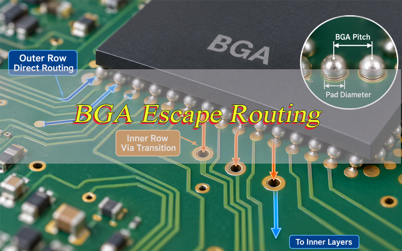
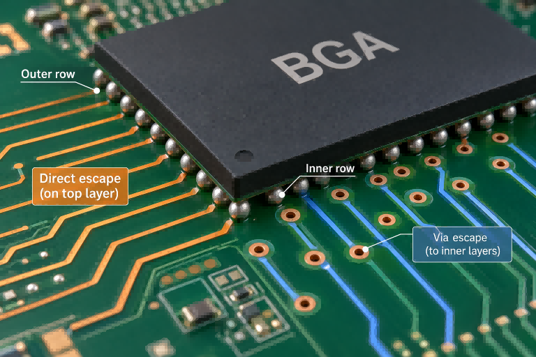
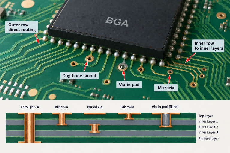
BGA escape routing is the process of bringing connections out of the BGA ball field so they can continue across the PCB. Outer ball rows can often escape directly on the component layer, while inner rows usually require vias to reach additional signal layers.
BGA fanout is one part of this process. Fanout describes the transition from a BGA pad to a trace or via, while BGA escape routing covers the complete breakout from the ball field into open routing space. As the pitch decreases and the row count increases, routing channels become narrower and the via strategy becomes more critical.
What Design Constraints Define a BGA Escape Routing Strategy?
Before choosing a fanout method, check the package geometry and PCB fabrication limits together:
- BGA pitch: Smaller pitch reduces the space available for traces and vias.
- Pad diameter: Larger lands leave narrower routing channels.
- Trace width and spacing: Determine how many traces can pass between pads.
- Via geometry: Large via pads can block inner-row escape paths.
- Via structure: Through-vias, blind vias, microvias, and via-in-pad structures provide different layer access.
- PCB stackup: Defines the available routing layers and reference planes.
- Fabrication limits: Set practical trace, spacing, drill, annular ring, and microvia rules.
These values cannot be optimized separately. A narrower trace does not solve the layout if the fanout vias still occupy the channel. Confirm the footprint, trace and spacing rules, via dimensions, and stackup before the BGA breakout is finalized.
How Does BGA Pitch Affect the Escape Routing Method?
BGA pitch determines how much room is available between adjacent lands. Larger-pitch packages usually provide enough space for conventional dog-bone fanout and mechanically drilled vias. As the pitch decreases, via pads and trace clearances begin competing for the same space.
| BGA Pitch | Typical Approach | Main Constraint |
|---|---|---|
| 1.27 mm | Dog-bone and through-via | Usually generous routing space |
| 1.0 mm | Dog-bone and through-via | Via and trace clearance |
| 0.8 mm | Optimized dog-bone or smaller via | Fewer routing channels |
| 0.65 mm | Small via, HDI, or via-in-pad | Inner-row access |
| 0.5 mm and below | Microvia and via-in-pad often considered | Very limited breakout space |
These are planning ranges rather than fixed rules. A simple 0.8 mm package may route with standard through-vias, while a dense FPGA at the same pitch may not. Ball count, number of rows, signal assignment, trace and spacing rules, and available routing layers matter as much as pitch.
How Do You Determine Whether Traces Can Pass Between BGA Pads?
Start with the physical space between adjacent PCB lands. If the ball pitch is P and the land diameter is D:
Available pad gap = P – D
For one trace to pass through that gap, the trace width plus twice the required clearance must fit within the available pad gap.
If two traces must share the same channel, the required trace-to-trace spacing must also be included. This simple check quickly shows whether the intended breakout is realistic before the full BGA fanout is created.
The calculation is only a starting point. Copper thickness, etching tolerance, registration, and actual fabrication capability reduce the usable margin. A trace that fits mathematically is not automatically a reliable production rule. Avoid designing every channel at the minimum trace and spacing limit unless the routing density requires it.
How Do You Route the Outer Rows of a BGA?
Outer rows normally provide the easiest paths out of the package. The goal is to use that advantage without blocking the deeper rows.
- Route directly outward where possible: Avoid unnecessary vias when a connection can remain on the component layer.
- Preserve inner routing channels: Do not fill valuable space with easy outer-row connections before the deeper rows are planned.
- Escape toward the destination: Route toward nearby memory, connectors, processors, or other ICs when placement is already defined.
- Keep sensitive nets short: Avoid unnecessary width changes and layer transitions.
Direct routing is useful, but it should still follow the complete BGA escape routing plan. The easiest connection should not occupy the only practical path available to a more constrained signal.
How Do You Escape the Inner Rows of a BGA?
Inner rows are blocked by surrounding balls, so most of their connections must transition to another layer before leaving the package area.
A practical sequence is:
- Plan the deepest rows first: Reserve their escape channels before easier signals use the available space.
- Move signals to internal layers: Use through-vias, blind vias, or microvias where appropriate.
- Assign layers by routing capacity: Do not rely on a fixed one-row-per-layer assumption.
- Reserve space for power and ground vias: These connections also consume breakout area.
- Change the via strategy when necessary: If conventional via pads occupy too much space, consider via-in-pad or microvias.
There is no universal rule that a certain number of BGA rows requires a fixed number of PCB layers. The required layer count depends on the actual pad, via, and trace geometry.
When Should You Use Dog-Bone Fanout for BGA Escape Routing?
Dog-bone fanout connects a BGA land to a nearby via with a short trace. It works well when the pitch provides enough room for the connection and the via pad does not block the channels required by surrounding signals.
This method is common with larger-pitch packages and many 1.0 mm or 0.8 mm BGAs because conventional drilled vias can often be used without pushing the PCB process to aggressive limits. It also keeps the via outside the solder land, simplifying fabrication compared with via-in-pad.
The limitation appears when the via field becomes denser than the available routing channels. Once conventional fanout vias begin blocking the paths required by deeper rows, via-in-pad or microvias are usually more effective than continuing to shrink the dog-bone geometry.
When Should You Use Via-in-Pad for BGA Escape Routing?
Via-in-pad becomes useful when a conventional fanout via occupies too much space beside the BGA land or prevents access to deeper rows. Placing the via directly in the land frees routing space between adjacent pads and allows an immediate layer transition.
This approach is common in fine-pitch FPGA, processor, SoC, memory, and other high-density BGA layouts. It can also shorten the pad-to-via transition for high-speed signals.
The via normally needs to be filled and planarized for BGA assembly. An open via inside the solder land can draw solder into the hole during reflow and reduce the solder volume at the joint. Via-in-pad therefore adds fabrication steps, but it is justified when it solves a real routing-density or signal-transition problem.
When Are Microvias Needed for Fine-Pitch BGA Escape Routing?
Microvias are used when conventional mechanically drilled vias occupy too much area. Their smaller geometry allows signals to move between nearby PCB layers while leaving more routing space for other connections.
They are especially useful in HDI BGA escape routing where via-in-pad is combined with blind microvias. Instead of carrying a large through-via through the entire stackup, a signal can transition only to the layer where it needs to be routed.
Microvias may be stacked or staggered depending on the layer structure and routing density. Their use should be driven by routing requirements rather than BGA pitch alone. If conventional vias still provide enough escape space, adding microvias only increases fabrication complexity.
How Many PCB Layers Do You Need for BGA Escape Routing?
Layer count depends on how many signals must leave the BGA and how much routing capacity each layer provides. Pitch alone cannot determine the required stackup.
A dense device may require more routing layers because of high ball count, limited trace channels, power and ground planes, controlled-impedance nets, differential pairs, and high-speed interfaces. Outer signals may remain on the component layer, while deeper rows move to different internal layers.
DDR, PCIe, USB, Ethernet, MIPI, and SerDes connections may also require specific reference planes, so their layer allocation cannot be based only on available routing space.
Use enough layers to complete the breakout without forcing the entire BGA area to minimum fabrication rules. In some designs, one additional signal layer provides better production margin than aggressive trace and via reduction across several layers.
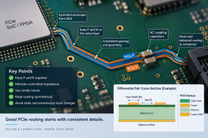
How Should You Escape Differential Pairs From a BGA?
Differential pairs should leave the BGA with similar geometry on both sides of the pair. Their breakout length, via type, antipad geometry, and reference environment should remain as consistent as the package allows.
If a layer transition is required, both members should normally use equivalent vias and share the same reference structure. Avoid giving one side an extra via or a significantly longer escape path.
Detailed length tuning is better performed once the pair reaches open board space. Inside the BGA field, maintaining pair symmetry and a clean return path is more useful than forcing exact length matching with unnecessary meanders.
For PCIe, USB, Ethernet, MIPI, and SerDes interfaces, the breakout should be planned together with controlled impedance, reference-plane continuity, and via transition design.
How Should Power and Ground Balls Be Handled During BGA Escape Routing?
Power and ground connections should be planned at the same time as the signal fanout. Leaving them until the end can create a breakout that works for signals but performs poorly for power delivery.
Power balls should have short connections to their planes, with enough via capacity for the expected current. Ground vias should also be available near high-speed signal transitions so the return current can follow a short path when a signal changes reference layers.
Decoupling capacitors affect the same area. Their connections should remain short and direct rather than being forced around an already congested fanout. Signal escape, power delivery, ground return, and decoupling placement should be treated as one routing problem.
What BGA Escape Routing Mistakes Should You Avoid?
Most BGA breakout problems result from using the available space in the wrong order or choosing geometry before checking the complete routing path.
- Oversized fanout vias: Block channels required by deeper rows.
- Unsupported trace and spacing rules: Create DFM problems or reduce production margin.
- Routing easy nets first: Can trap inner-row signals.
- Open via-in-pad: Can draw solder away from the BGA joint.
- Late stackup definition: Forces routing and reference-plane changes later.
- Too many layer transitions: Add vias and high-speed discontinuities.
- Broken return paths: Increase signal integrity and EMI risk.
- Poor differential symmetry: Introduces unnecessary skew.
- Blocked power access: Leaves insufficient room for power and ground vias.
- Minimum rules everywhere: Makes production less tolerant of normal process variation.
Solve the most constrained areas first, then use the remaining channels for less difficult connections.
What Should You Verify Before Releasing a BGA PCB for Fabrication?
Passing PCB DRC is not enough. The completed BGA escape routing should also match the intended fabrication and assembly process.
- BGA footprint: Verify pitch, pad diameter, orientation, and solder mask geometry.
- Trace and spacing: Check the smallest neck-down and copper clearance.
- Via geometry: Verify drill diameter, pad size, annular ring, antipad, and layer span.
- Via-in-pad: Confirm filling, plating, and planarization requirements.
- Microvias: Verify the layer span and stacked or staggered construction.
- PCB stackup: Check routing layers, dielectric thickness, and reference planes.
- High-speed nets: Verify impedance, differential symmetry, and return paths.
- Power delivery: Check plane access, via quantity, and decoupling paths.
- Manufacturing margin: Maintain sufficient tolerance beyond absolute process limits.
For HDI, fine-pitch BGA, via-in-pad, and microvia designs, a DFM review before fabrication can identify breakout and stackup conflicts before they reach production.
FAQs About BGA Escape Routing
Q1: Can FPGA pin swapping make BGA routing easier?
A1: Yes, when the FPGA architecture allows it. Reassigning compatible I/O pins can reduce trace crossings and improve escape direction. Pin changes must still respect I/O banks, voltage domains, differential-pair assignments, clock-capable pins, and device-specific restrictions.
Q2: Should unused or NC BGA balls still have PCB pads?
A2: Usually yes. Follow the recommended land pattern unless the component documentation allows a change. Removing an NC pad only to create more routing space may affect assembly or future device compatibility. Do not alter the footprint without package-specific guidance.
Q3: Does copper thickness affect BGA breakout capability?
A3: Yes. Heavier copper generally requires more allowance during etching, making very fine trace and spacing geometry harder to produce. Copper thickness should be considered when setting routing rules beneath a dense BGA.
Q4: Does solder mask design matter around BGA pads?
A4: Yes. Solder mask registration and pad definition affect the usable area around each land. The mask design should support reliable assembly while maintaining realistic fabrication tolerance. Do not reduce mask clearances only to gain routing space.
Q5: Can BGA escape traces use a local neck-down?
A5: Yes. A short neck-down can help a trace pass through a restricted breakout channel and then return to its normal width outside the BGA. Keep the narrow section short and check its impedance or current-carrying requirements where relevant.
Q6: Should test points be placed inside the BGA breakout area?
A6: Usually not unless the available space clearly supports them. Test pads consume routing space and can increase congestion around already constrained signals. Place test access outside the dense ball field whenever practical.
Q7: Can thermal vias interfere with BGA routing?
A7: Yes. Thermal vias near the package can occupy channels required by signals, power, or ground connections. Plan thermal management and BGA routing together so thermal structures do not block critical breakout paths.
Q8: Does BGA breakout affect EMI performance?
A8: It can. Long escape paths, poor reference continuity, unnecessary layer changes, and large return loops can increase unwanted radiation. Short routes and continuous return paths help reduce EMI risk around high-speed BGA interfaces.
Q9: Can buried vias reduce congestion around a BGA?
A9: Yes. Buried vias connect internal layers without occupying every layer in the PCB stackup, which can free routing space elsewhere. They also increase fabrication complexity, so use them only when the routing benefit justifies the additional process steps.
Q10: How does nearby component placement affect BGA routing?
A10: Placement determines where major signal groups should leave the package. Memory, connectors, decoupling capacitors, and adjacent ICs should be positioned so related nets can escape in useful directions. Good placement can reduce crossings, vias, and unnecessary routing length.
Q11: Can BGA congestion be reduced before routing begins?
A11: Yes. Review the pin map, interface direction, component placement, stackup, and signal grouping before detailed fanout. Programmable devices may also allow legal pin reassignment. Early planning is usually more effective than repairing blocked routes later.
Q12: Does dense BGA routing make rework harder?
A12: It can. Fine pitch, via-in-pad, dense neighboring components, and limited access can all increase rework difficulty. Adequate component clearance and stable pad and via construction help reduce rework risk.
Conclusion
Effective BGA escape routing depends on available routing space, via geometry, and PCB stackup. Plan the inner rows first, use conventional fanout where it fits, and move to via-in-pad or microvias when routing density requires them.
For fine-pitch BGA, HDI, via-in-pad, microvia, or high-layer-count PCB projects, EBest Circuit can review your Gerber files, stackup, BGA pitch, via structure, and impedance requirements before production. Contact sales@bestpcbs.com for technical review and quotation.