





Pin in Paste is a through-hole reflow method that solders compatible THT components during the same oven cycle used for surface-mount parts. It can remove a separate wave, selective, or hand-soldering operation, but only when the component, plated hole, solder volume, stencil, and reflow profile are designed as one process. The method is most useful on mixed-technology assemblies with a limited number of reflow-compatible connectors or other through-hole parts.
A successful result is not created by simply printing paste over a hole. The design process must calculate the metal required to fill the annular space around each pin, convert that requirement into printable solder-paste volume, confirm that the stencil can release the deposit, and verify that insertion does not push the paste out of position. Production then needs a profile that satisfies the solder paste, the PCB, the SMT population, and the THT component housing.
What Is Pin in Paste Technology in PCB Assembly?
Pin in Paste technology places solder paste at a plated through-hole before a component lead is inserted, allowing the joint to form during reflow. The method is also called PiP, paste-in-hole, through-hole reflow, or intrusive reflow soldering. These names describe the same basic objective: integrating suitable through-hole components into an SMT production flow.
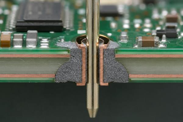
The paste may be deposited around the annular pad, partly into the hole, or over a controlled area of solder mask. When the assembly reaches reflow temperature, the solder alloy melts and wets the component lead, annular pad, and plated barrel. Surface tension draws available solder toward solderable surfaces, while the flux removes oxides and supports wetting. After cooling, the joint should provide the required electrical connection and mechanical support without bridging, insufficient fill, or contamination.
The strongest application is normally a predominantly SMT board containing a small number of THT connectors, relays, switches, transformers, or capacitors that can tolerate the selected reflow profile. Pin in Paste becomes less attractive when the board has many large THT parts, when the required metal cannot be delivered through the available stencil area, or when component housings cannot withstand reflow.
How Does the Pin in Paste Soldering Process Work?
The Pin in Paste soldering process follows the SMT line, but each stage must account for the larger paste deposit and the mechanical action of inserting a lead through it.
- Review the assembly. Identify every THT part proposed for reflow. Check the manufacturer’s peak-temperature limit, permitted time above liquidus, housing material, stand-off, pin geometry, coplanarity, moisture requirements, and insertion method.
- Calculate the solder requirement. Determine the free plated-hole volume around the pin, include the intended fillets, and convert the required metal volume into solder-paste volume using the paste supplier’s metal-volume data.
- Design the PCB and stencil together. Set finished-hole size, annular pad, solder-mask opening, lead protrusion, stencil thickness, and aperture geometry. Confirm that overprint does not interfere with adjacent pads, vias, test points, or the component body.
- Print the solder paste. Deposit paste through the stencil. Larger PiP apertures may need split patterns or local stencil thickness changes to improve release and control where the paste enters the hole.
- Inspect the print. Check paste position, volume, smearing, bridging, and paste visible on the opposite side. A process that already shows unstable deposits before insertion will not become more stable after insertion.
- Insert the THT component. Place the part manually or with automated insertion equipment. Control insertion speed and alignment so the pin does not sweep paste away, force it into a connector contact, or leave the housing tilted.
- Reflow the assembly. Use a measured thermal profile that remains inside the solder-paste and component limits. The paste melts, wets the barrel and pin, and pulls back from non-solderable mask areas.
- Inspect and qualify the joint. Apply visual inspection first. Use X-ray when hidden conditions cannot be assessed externally, and use cross-section analysis when qualification or unresolved risk requires direct internal evidence. Confirm the profile and inspection plan before releasing volume production.
When Should You Choose Pin in Paste Instead of Wave or Selective Soldering?
Choose Pin in Paste when the board is mainly SMT, the remaining THT parts can survive reflow, and a printable deposit can provide the required solder. Wave and selective soldering remain valid alternatives when component thermal limits, THT density, bottom-side geometry, or solder-volume requirements make intrusive reflow difficult.
| Dimension | Pin in Paste | Wave Soldering | Selective Soldering | Decision |
| Best assembly mix | Mostly SMT; few suitable THT parts | Many accessible THT joints | Localized THT joints | Count and map all THT locations |
| Thermal exposure | Full reflow profile | Bottom side contacts solder wave | Localized solder fountain | Use component temperature limits |
| Solder delivery | Stencil, jet, or preform | Molten solder wave | Programmed nozzle | Verify achievable barrel fill |
| Design sensitivity | High: hole, pin, stencil, spacing | Masking and solder-side access | Nozzle access and keep-outs | Review the actual layout |
| Extra process | Integrated reflow; insertion still required | Separate line operation | Separate programmed operation | Compare total process risk |
| Typical limitation | Paste volume or heat-sensitive parts | Thermal load and masking | Cycle time and access | Select by constraints, not fashion |
Do not select a method from equipment cost alone. A single reflow pass can simplify routing, but an unstable PiP joint may create inspection, rework, and field-risk costs that exceed the saved operation. The correct comparison includes process capability, first-article qualification, fixture or masking needs, cleaning, takt time, maintenance, inspection access, and the cost of recovering a marginal connector joint.
Which Pin in Paste Connectors and THT Components Are Reflow-Compatible?
A connector is Pin in Paste compatible only when the complete component—not merely its metal pins—can withstand the planned profile and insertion process. Review the exact manufacturer part number because similar connector families may use different housing resins, plating systems, packaging, or stand-offs.
- Temperature rating: Confirm peak body temperature and permitted exposure duration against the measured board profile.
- Housing stability: Check for softening, warpage, blistering, discoloration, or dimensional movement during reflow.
- Stand-off: There must be enough clearance for the paste deposit and fillet without allowing solder or flux residue to reach prohibited housing surfaces.
- Pin geometry: Review cross-section, plating, length, taper, shoulder, retention features, and internal openings that could draw solder by capillary action.
- Coplanarity and retention: The component must sit correctly before and during reflow. Uneven seating can create inconsistent insertion depth and paste displacement.
- Moisture handling: Follow the component supplier’s storage, floor-life, and baking instructions where applicable.
Modular jacks and D-sub connectors are common search examples, but their names do not prove compatibility. A shielded modular jack may contain a plastic housing, shield tabs, signal pins, and retention posts with different thermal and solder requirements. The review must therefore cover every lead group and the final assembly orientation.
What Pin in Paste PCB Design Rules Control Hole Size, Pin Clearance and Lead Protrusion?
The critical PCB design task is balancing insertability against solder demand. A large finished hole makes insertion easier but increases the annular volume that must be filled. A very tight hole reduces solder demand but may create interference when pin size, hole plating, drilling, component position, and insertion accuracy reach their worst-case limits.
- Start with finished dimensions. Use the finished plated-hole diameter, not the drill-tool diameter. Use the component manufacturer’s pin maximum and minimum dimensions rather than a nominal value alone.
- Build the tolerance chain. Include finished-hole tolerance, pin tolerance, pin position, hole position, connector coplanarity, and insertion-equipment accuracy.
- Confirm insertion clearance. The worst-case smallest hole must accept the worst-case largest and most displaced pin without damaging the plating or component.
- Calculate solder demand. Use the worst-case free volume that must be filled, then include the selected fillet allowance and process margin.
- Control lead protrusion. Excessive protrusion can displace paste during insertion and wick solder away from the barrel. Insufficient protrusion can make inspection and fillet formation difficult.
- Check surrounding space. Reserve room for the aperture or overprint while protecting neighboring SMT pads, vias, solder-mask dams, test points, and component bodies.
- Document the intent. Show special paste apertures in the paste data and identify PiP parts in assembly notes. Do not expect the manufacturer to infer the process from a standard through-hole footprint.
No universal clearance number fits every connector. Round, square, rectangular, compliant, and forked pins occupy different volumes and behave differently during insertion and heating. The final value should be approved through a tolerance review and first-article evidence rather than copied from a generic rule.
How Do You Calculate Pin in Paste Solder Volume?
A Pin in Paste calculator estimates how much paste is required by comparing the plated-hole volume with the pin volume and the desired fillets. For a round hole and round pin passing through board thickness H, a useful starting model is:
Required solder metal volume = plated-hole volume − pin volume + fillet allowance.
The cylindrical hole volume is πR²H, while the cylindrical pin volume is πr²H. Square or rectangular pins require the correct cross-sectional area instead of a circular approximation. After calculating the metal volume, convert it into paste volume:
Required solder-paste volume = required metal volume ÷ solder paste metal fraction by volume.
Metal percentage by weight is not the same as metal percentage by volume. Use the solder-paste supplier’s technical data or process guidance. The aperture must also release the intended deposit, so theoretical aperture volume must be adjusted for actual transfer efficiency. Paste type, aperture area ratio, stencil coating, print speed, squeegee settings, board support, and environmental control can all change the delivered amount.
For an illustrative calculation, assume a round finished hole of 1.20 mm, a round pin of 0.80 mm, and a 1.60 mm board. The free cylindrical volume is π × (0.60² − 0.40²) × 1.60, or approximately 1.01 mm³ before adding fillet volume. If the selected paste provides 50% metal by volume, the starting paste requirement for the barrel portion would be approximately 2.02 mm³. The stencil design must then provide this volume plus the defined fillet allowance, adjusted for measured transfer efficiency.
This example is a calculation method, not a production specification. Actual projects must use finished dimensions, real pin geometry, selected paste data, process capability, and inspection results.
What Pin in Paste Stencil Design Rules Control Solder Volume and Hole Fill?
The stencil must deliver sufficient paste without creating an unstable print, obstructing insertion, or contaminating nearby features. Standard SMT stencil thickness may not provide enough local volume, so the aperture strategy should be selected only after the solder calculation is complete.
- Overprint: Extend the aperture beyond the solderable pad onto a controlled solder-mask area. During reflow, molten solder should pull back toward the pad and barrel. Available space, solder-mask surface behavior, paste wetting, and neighboring features limit the extension.
- Split apertures: Divide a large deposit into controlled segments to improve print stability, reduce scooping, and manage where the pin contacts the paste.
- Step stencil: Use a locally thicker region when the PiP deposit cannot be delivered through the base stencil. The step must remain compatible with nearby fine-pitch SMT printing and squeegee travel.
- Jet printing: Add paste locally without increasing the thickness of the entire stencil. Cycle time, deposit repeatability, paste compatibility, and equipment access must be evaluated.
- Solder preforms: Add controlled metal volume when paste alone is impractical. Preforms contain far more metal by volume than solder paste and can reduce dependence on very large overprints, but placement, flux, geometry, and cost require validation.
The best strategy may combine a moderate overprint with a step, jet deposit, or preform. More paste is not automatically better: excessive volume can bridge pins, contaminate a connector, increase flux residue, or fall through the hole before melting.
How Should Pin in Paste Reflow Profiles and Solder Paste Be Selected?
The correct profile must satisfy the solder paste, the entire component population, the PCB thermal response, and the reflow oven. Begin with the paste supplier’s process window and the component manufacturers’ limits, then measure the actual assembly with thermocouples at thermally significant and sensitive locations.
Paste properties have a direct effect on PiP stability. Strong tack helps retain the larger deposit before reflow. Good hot-slump resistance reduces the tendency to flow or fall through the barrel during heating. Wetting performance supports pullback from solder mask and filling of the plated barrel. Flux chemistry and residue level affect inspection, in-circuit test contact, cleaning requirements, and contamination around connector housings.
A fast initial ramp may lower paste viscosity too quickly and increase drop-through risk. Excessive time at elevated temperature can stress component housings and consume flux activity. Too little time above liquidus can leave incomplete wetting, while excessive peak temperature can damage heat-sensitive parts. These interactions are why a generic profile should never replace measured profiling on the actual assembly.
What Pin in Paste DFM Checks Should Be Completed Before Production?
A Pin in Paste DFM review should confirm that component, PCB, stencil, insertion, reflow, and inspection requirements form one executable plan. The review must also distinguish industry guidance from the assembly supplier’s verified PCB Manufacturing Capability. Complete the following checks before stencil release or volume ordering:
- Verify complete component part numbers and obtain current manufacturer datasheets.
- Confirm reflow-temperature limits, exposure time, moisture handling, housing material, stand-off, pin geometry, and packaging.
- Review Gerber or ODB++ data, finished-hole sizes, plating, board thickness, surface finish, solder mask, and dimensional tolerances.
- Check pin-to-hole tolerance at worst-case conditions and verify insertion equipment or manual access.
- Calculate required solder metal and paste volume for each distinct pin and hole geometry.
- Review stencil thickness, aperture shape, overprint area, split apertures, step regions, jet deposits, or preforms.
- Check nearby SMT pads, vias, test points, solder-mask dams, component bodies, and bottom-side restrictions.
- Define component retention, insertion depth, lead protrusion, and controls against tilting or floating.
- Establish a measured reflow-profile plan covering heavy and thermally sensitive locations.
- Define SPI, visual, X-ray, cross-section, electrical, and functional inspection requirements according to project risk.
- Plan first-article acceptance and document what evidence is required before volume release.
- Confirm that PiP remains lower risk than wave, selective, or hand soldering for the actual assembly.
The quotation package should include fabrication data, drill data, BOM, placement files, assembly drawings, connector datasheets, product class, expected quantity, inspection requirements, and any project-specific barrel-fill or cleanliness criteria. Missing inputs force assumptions at the exact points where PiP is least tolerant of assumptions.
What Causes Incomplete Hole Fill, Bridging, Voids or Connector Movement?
Most Pin in Paste defects trace back to a mismatch among free hole volume, delivered paste, insertion behavior, wetting, and the thermal profile. Corrective action should begin with evidence rather than immediately increasing the aperture.
| Defect | Likely Causes | Verification | Corrective Direction |
| Incomplete fill | Low paste volume; large clearance; poor wetting; solder wicking | Recalculate volume; inspect print; X-ray or cross-section | Correct hole, aperture, paste, surface, or profile |
| Bridging | Excess overprint; close spacing; slump; displaced paste | SPI and visual inspection before and after insertion | Split or reduce aperture; improve mask and insertion |
| Voids | Flux outgassing; geometry; contamination; profile | X-ray; cross-section when required | Adjust deposit, materials, cleanliness, or profile |
| Paste drop-through | Excess hole fill; weak tack or hot slump; rapid heating | Bottom-side print check; oven contamination trend | Control hole entry, paste properties, and heating |
| Connector movement | Poor retention; coplanarity; uneven wetting; insertion error | Placement measurement and post-reflow inspection | Improve fixture, aperture balance, or insertion control |
| Solder in contacts | Pin structure; capillary flow; insertion pushes paste inward | Internal inspection and mating/function test | Limit in-hole paste or use a controlled preform |
When a joint fails, preserve the print, insertion, profile, and inspection data from the same assembly. A cross-section without paste-volume or profile evidence may show the result but not the cause. Conversely, an acceptable SPI reading does not prove that the pin retained the intended paste after insertion.
How Should Pin in Paste Solder Joints Be Inspected and Accepted?
Inspection should verify both the manufacturing process and the final joint. No Pin in Paste-only standard defines every design, process, and acceptance input. Acceptance must therefore follow the specified product class, drawing, contract requirements, and applicable workmanship criteria established before production.
- Inspect the paste print. Verify deposit position, repeatability, smearing, bridging, and bottom-side drop-through before component insertion.
- Inspect component insertion. Confirm seating, orientation, retention, protrusion, and whether insertion displaced the deposit.
- Verify the thermal profile. Record actual temperatures at representative heavy joints and temperature-sensitive parts.
- Perform visual inspection. Check visible fillets, wetting, bridging, solder balls, residues, housing clearance, and component alignment.
- Use X-ray where needed. Screen solder distribution, internal voiding, and hidden bridging when the joint geometry and viewing angle allow a useful image.
- Use cross-sections for qualification or unresolved risk. Cross-sections directly show barrel wetting and internal fill, but they are destructive and should follow a defined sampling plan.
- Complete electrical and functional checks. Connector mating, retention, continuity, isolation, and application-specific functions may reveal defects that appearance alone cannot detect.

Trend data is as important as a single accepted sample. Monitor printed volume, profile drift, defect type, rework, residue, oven contamination, and connector function. A stable process should demonstrate repeatability across normal material, component, and equipment variation.
FAQs About Pin in Paste Technology in PCB Assembly
Q1. What Is Another Name for Pin in Paste Soldering?
A1. Pin in Paste is also called PiP, paste-in-hole, intrusive reflow, through-hole reflow, or pin-in-hole reflow. Terminology varies by component supplier and assembly company, but the common principle is applying solder paste to a plated through-hole and forming the THT joint during the SMT reflow cycle.
Q2. Can Every Through-Hole Connector Use Pin in Paste?
A2. No. The exact connector must tolerate the measured reflow profile and provide suitable stand-off, pin geometry, coplanarity, retention, and insertion clearance. Similar-looking connector families may use different plastics or plating. Always check the complete manufacturer part number and its approved processing conditions.
Q3. Does Pin in Paste Always Require a Step Stencil?
A3. No. A standard stencil may work when the required solder volume is modest and enough overprint area is available. A step stencil becomes useful when local PiP volume exceeds what the base stencil can deliver. Nearby fine-pitch SMT deposits and printing behavior must remain acceptable.
Q4. When Are Solder Preforms Needed for Pin in Paste?
A4. Preforms are considered when stencil overprint or local thickness cannot supply sufficient metal without creating bridging or print instability. Because a preform is predominantly solder metal rather than flux-rich paste, it can add controlled volume in less space. Placement, geometry, flux compatibility, and cost still require qualification.
Q5. How Much Solder Paste Should Be Printed Into the Through-Hole?
A5. The amount depends on finished-hole volume, pin volume, board thickness, fillet target, paste metal fraction, transfer efficiency, and insertion displacement. Filling the hole completely with paste before insertion is not a universal goal and may increase drop-through or displacement. Use a calculation followed by first-article verification.
Q6. What Causes Solder Paste to Fall Through a Plated Hole?
A6. Common causes include excessive paste placed directly over the opening, low tack, weak hot-slump resistance, unsuitable print geometry, vibration during handling, and rapid viscosity reduction during heating. A stencil bar or divided aperture can limit direct hole loading while maintaining total paste around the pad.
Q7. How Much Barrel Fill Is Acceptable for a Pin in Paste Joint?
A7. Acceptance depends on the applicable product class, project requirements, lead and termination conditions, and the workmanship standard invoked by the drawing or contract. Do not use one percentage as a universal rule. Define the requirement before production and choose an inspection method capable of confirming it.
Q8. Can Pin in Paste Be Used With Lead-Free Solder Paste?
A8. Yes, provided the connector, PCB, other components, paste, and profile are compatible. Lead-free processes often use higher thermal exposure than traditional tin-lead processing, making housing stability and profile verification especially important. Low-temperature alloys may be considered only when their reliability and application limits are acceptable.
Q9. How Should Pin in Paste Apertures Be Shown in PCB Design Files?
A9. Put the intended apertures in the paste-layer data and identify the affected reference designators in assembly documentation. Include any overprint, split-aperture, step-stencil, jet, or preform requirements. The manufacturer should not have to infer a special process from a conventional through-hole footprint.
Q10. Which Files Are Required for a Pin in Paste DFM Review?
A10. Provide Gerber or ODB++, drill data, finished-hole requirements, BOM, placement files, assembly drawings, complete connector datasheets, board thickness, tolerances, surface finish, product class, quantity, and inspection requirements. Include project-specific solder-fill, cleanliness, reliability, and functional-test criteria. Clearly identify every reference designator intended for the Pin in Paste process.
Pin in Paste can simplify a mixed SMT and THT assembly, but reliable implementation depends on coordinated component selection, PCB geometry, solder-volume calculation, stencil design, insertion control, reflow profiling, and inspection. Treating these decisions as one DFM system is the most effective way to prevent insufficient fill, bridging, voiding, connector movement, and avoidable rework.
If you are planning a mixed-technology PCB assembly and need a Pin in Paste DFM review, contact EBest Circuit. Send your PCB data, BOM, assembly drawings, connector datasheets, production quantity, and inspection requirements to sales@bestpcbs.com for a DFM review and quotation.
You may also like








Tags: pin in paste defects, pin in paste design rules, pin in paste solder volume, pin in paste stencil design