PCB manufacturing PCB manufacturing
Home > Blog

robotics pcb assembly

AI Robotics PCB Manufacturing and Assembly Services from Prototype to Mass Production
Friday, August 21st, 2026

AI robotics PCB manufacturing brings computing, vision, sensing, motion control, communications, and power electronics into one hardware program. A computing board may require dense BGA breakout and controlled impedance, while motor-control and power-distribution boards must carry pulsed current without disturbing sensors or data links.

Prototype success does not guarantee repeat production. Mixed file revisions, unavailable processors, fine-pitch solder defects, motor-related power noise, concentrated heat, and incomplete test limits can cause rework, inconsistent builds, or delayed product validation.

EBest Circuit reviews the complete manufacturing package. We align PCB data, BOM, placement, assembly, programming, inspection, and customer-defined test requirements before production, then support fabrication and assembly from prototype through volume builds. Send your Gerber/ODB++, BOM, quantity, assembly files, and test scope to sales@bestpcbs.com for a free DFM review and quotation.
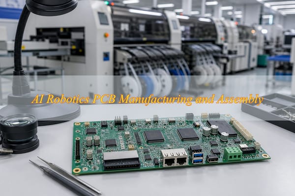
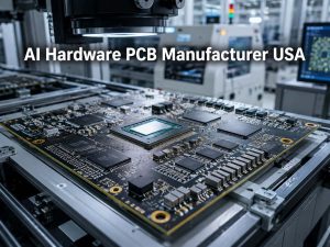
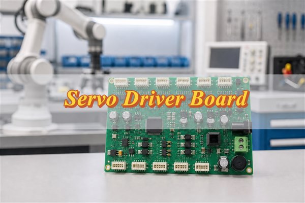
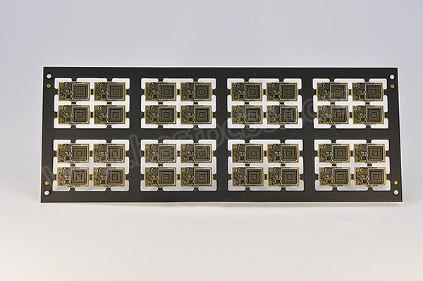
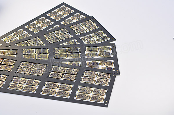
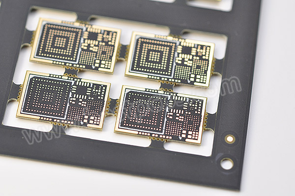
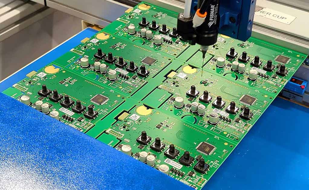
AI robotics PCB manufacturing, assembled robot controller PCB on an electronics production workbench

What Types of PCBs Are Used in AI Robotics Systems?

Board partitioning should follow system function. An AI robotics system may distribute computing, sensing, motion, power, and communication across several PCBs or combine selected functions on one board. Common PCB categories include:

PCB Type Main Function Typical Requirements
AI computing PCB Runs AI inference, control algorithms, and data processing Dense BGA routing, high-speed interfaces, controlled impedance, thermal management
Vision PCB Connects cameras and image sensors High-speed interfaces, low-noise power, compact layout
Sensor PCB Collects encoder, IMU, force, distance, or environmental data Low-noise analog circuits, stable references, reliable sensor interfaces
Robot control PCB Coordinates motion, I/O, and communications MCU/FPGA integration, CAN/Ethernet interfaces, mixed-signal layout
Motor control PCB Drives BLDC motors, servos, and other actuators Higher current, MOSFET thermal paths, reinforced power connections
Power distribution PCB Converts and distributes battery or DC input power Current-carrying capacity, power connectors, protection devices, thermal control
Communication PCB Handles wired or wireless links Controlled impedance, RF requirements, connector and antenna constraints

A humanoid robot may place motor-control boards close to individual joints while keeping AI computing and vision processing in the head or torso. An autonomous mobile robot may use a central computing board connected to separate motor, navigation, power, and communication boards.

The exact architecture depends on processing load, mechanical space, cable length, current distribution, and serviceability. Before releasing each board, verify its power budget, interface ownership, connector path, mounting envelope, and replacement boundary; an unclear split can create overloaded connectors, duplicated power conversion, or interfaces that cannot be tested independently.

Which Components and Interfaces Are Commonly Used on AI Robot PCBs?

Package mix and interface speed drive PCB complexity. AI robot PCBs may combine processors, memory, sensors, power devices, and communication circuits whose electrical, assembly, and test-access requirements must be reviewed together.

Common components include:

  • AI processors and SoCs: Run computer vision, neural-network inference, navigation, and higher-level decision functions.
  • MCUs and FPGAs: Handle real-time I/O, timing-sensitive control, motion functions, and interface management.
  • DDR memory and flash storage: Support high-bandwidth processing and local data storage.
  • Image sensors and camera-related ICs: Support RGB, depth, stereo, and machine-vision systems.
  • IMUs and motion sensors: Measure acceleration, angular rate, orientation, or movement.
  • Motor drivers and MOSFETs: Switch current for BLDC motors, servos, pumps, and actuators.
  • Encoders and feedback devices: Provide position, speed, and motion feedback.
  • DC-DC converters and regulators: Generate stable power rails for processors, sensors, and communication circuits.

Common interfaces include:

  • CAN and CAN-FD: Connect distributed motor and control nodes.
  • Ethernet: Carries higher-bandwidth data between computing and control modules.
  • USB: Supports peripherals, cameras, configuration, and data transfer.
  • PCIe: Supports high-bandwidth expansion or computing modules where the architecture requires it.
  • High-speed camera interfaces: Carry image and vision data between sensors and processors.
  • Wi-Fi and Bluetooth: Support wireless communication, configuration, and telemetry.

For engineering and sourcing teams, the important cost and schedule drivers are package pitch, routing density, current, and interface speed rather than the total component count. Include these constraints in the RFQ so suppliers quote the required stackup, inspection, and assembly route instead of pricing from board dimensions alone.

Which PCB Technologies Are Needed for AI Processors, Vision Sensors, and Motion Control?

Each robot function owns different PCB requirements. AI processing is dominated by BGA breakout, memory routing, power integrity, and heat; machine vision by low-noise power and camera-link continuity; and motion control by pulsed current, switching loops, protection, and thermal paths.

  • AI processor and memory routing: Start from the released processor escape pattern, DDR topology, interface constraints, and stackup. Use HDI, laser microvias, or filled via-in-pad only when the BGA pitch and routing channels cannot be completed with a simpler through-via structure. Verify impedance coupons where specified and review the routed design for reference-plane continuity and excessive via transitions before fabrication.
  • Processor power integrity: Separate core, memory, I/O, and auxiliary rails according to the processor power tree. Place the required decoupling close to the relevant power balls, provide low-impedance return paths, and size regulator and copper paths for startup and workload transients. Validate rail sequencing, ripple, droop, and current at defined operating states rather than checking only idle voltage.
  • Processor thermal path: Move package heat into the PCB copper, thermal vias, heat spreader, or chassis interface defined by the mechanical design. Confirm thermal-pad solder coverage and interface contact during assembly, then measure component temperature under sustained inference and communication loads to check throttling margin.
  • Vision sensor signal path: Route MIPI, LVDS, USB, Ethernet, or other camera links to their specified impedance, skew, and reference requirements. Maintain a continuous return structure across connectors and layer transitions, and keep camera clocks and data pairs away from motor-switching nodes. Verify the interface with captured images and error monitoring under representative cable length and frame rate.
  • Vision sensor power and grounding: Supply image sensors, clocks, and analog references from low-noise rails with local filtering and decoupling placed at the receiving devices. Keep shared impedance with motor and power-conversion returns out of the sensor reference path. Compare image noise, dropped frames, and sensor data with motors disabled and operating to identify coupling.
  • Motion-control power stage: Size MOSFET, driver, shunt, connector, copper, and plated transitions from continuous current, peak current, duty cycle, and fault-clearing requirements. Keep the switching and gate-drive loops compact, separate sensitive encoder and communication routes, and provide a defined heat path from the power devices. Validate current waveform, rail disturbance, device temperature, and protection response at startup, reversal, braking, stall, and commanded load changes.

Assign each requirement to one board function and one verification method so computing, vision, and motion-control rules are not copied across unrelated boards.

How Should Robot Control PCBs Handle Motor Current, Power Noise, and Signal Integrity?

A robot control PCB must prevent motor and actuator loads from disturbing processors, sensors, and communication circuits. Current changes during motor startup, braking, reversal, and torque changes can create voltage drop, switching noise, and ground disturbance.

  • Current-path sizing: Size power traces and copper areas from both continuous and peak current so the conductors match the actual load.
  • Layer-change capacity: Use sufficient copper and plated connections where current changes layers to avoid narrow current bottlenecks.
  • Switching-loop control: Keep high-current switching loops compact around MOSFETs, motor drivers, and local decoupling to reduce conducted and radiated noise.
  • Power and signal separation: Route motor-current paths away from low-level analog and sensor circuits to reduce measurement disturbance.
  • Return-path continuity: Maintain continuous return paths under high-speed signals so return current does not detour around plane gaps.
  • Bulk energy storage: Place bulk capacitance close to high-current loads to limit supply collapse during rapid load changes.
  • Local high-frequency decoupling: Place local decoupling close to processors, drivers, and interface ICs to reduce high-frequency supply noise.
  • Connector current limit: Check connector current rating together with PCB copper capacity because an undersized connector can become the limiting point.
  • Sensitive-node clearance: Keep switching nodes away from encoder inputs, analog sensors, clocks, and sensitive communication lines.

A controller that operates normally on a bench may reset when several motors accelerate together. Power-rail drop, connector resistance, inadequate bulk capacitance, or poor current return paths should be checked before treating the problem as a processor or firmware failure.

How Are HDI PCBs for AI Robotics Manufactured?

Specify HDI only when the routed design needs it. Engineers should confirm that through vias cannot complete the BGA breakout or high-speed routing. Procurement should compare the proposed microvia structure, lamination count, via fill, registration plan, test evidence, and repeat-production controls.

The released stackup should identify core and prepreg construction, finished copper, dielectric spacing, impedance requirements, microvia layers, and permitted via structures. These inputs let the supplier confirm manufacturability and allow the buyer to see which fabrication steps and inspections are included in the quotation.

  • Microvia structure: State the start and stop layers, finished diameter, pad size, and whether the vias are staggered, stacked, filled, or capped. This prevents different suppliers from quoting different constructions under the same HDI label.
  • Via-in-pad requirement: Identify the BGA, LGA, or thermal-pad locations that require filling and planarization. Ask the supplier to confirm the fill and surface preparation included in the build.
  • Lamination count: Request the proposed build sequence when several drilling and lamination cycles are required. Additional cycles affect cost, lead time, registration risk, and the ease of repeating the design.
  • Fine-line capability: Compare the released trace, space, annular-ring, and registration requirements with the supplier’s reviewed manufacturing limits for this stackup rather than relying on a general capability table.
  • Plating evidence: Define the required finished copper and hole requirements and agree on the coupon, microsection, or inspection evidence needed for lot acceptance.
  • Impedance verification: Provide target values, tolerances, reference layers, and coupon requirements. Request the measured coupon result when controlled impedance is part of the order.
  • Registration review: Ask for a DFM response covering microvia-to-pad alignment and layer-to-layer registration where the design uses tight capture pads or stacked structures.
  • Bare-board release: Include electrical testing for opens and shorts and define any additional dimensional, impedance, or microsection records required before assembly.

Request a reviewed stackup before tooling. If a simpler via structure completes the routing, remove unnecessary lamination cycles, cost, and supply risk.

What Assembly Controls Are Required for AI Processors, BGAs, Memory, and Fine-Pitch Components?
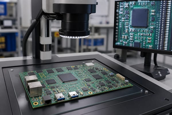
AI robotics PCB manufacturing, microscope inspection of a fine-pitch robot controller PCBA

Fine-pitch packages need an agreed assembly and inspection plan. Engineers should identify package-specific risks, while procurement should confirm which controls and records are included in the quotation for processors, DDR devices, QFNs, LGAs, BGAs, and small passive components.

  • Package-data confirmation: Supply manufacturer part numbers, approved footprints, polarity, and package drawings. Require discrepancies to be raised before stencil or placement-program release.
  • Moisture-sensitive handling: Identify moisture-sensitive devices and request handling records when storage exposure or baking can affect package integrity and solderability.
  • Stencil review: Ask the assembler to review stencil thickness and critical apertures against the complete package mix, especially when a large thermal pad sits beside fine-pitch passives.
  • Paste inspection scope: Define whether SPI is required for the pilot and production lots and which paste defects or trends must stop the build before placement.
  • First-article evidence: Agree on the component identity, polarity, placement, and workmanship checks that must be completed before the balance of the lot proceeds.
  • Reflow confirmation: Request confirmation that the profile is developed around board thermal mass, solder-paste requirements, and component temperature limits.
  • Hidden-joint inspection: Specify X-ray coverage and acceptance criteria for BGA, LGA, QFN, and other bottom-terminated packages that AOI cannot assess.
  • Thermal-pad acceptance: Define how solder coverage or voiding beneath exposed pads will be evaluated when it affects heat transfer or electrical grounding.
  • Mixed-technology assembly: Identify press-fit, selective-soldered, or manually installed power connectors so their tooling, sequence, and inspection are included in the quote.

For a valid price comparison, require each supplier to state the SPI, AOI, X-ray, first-article, programming, and test scope. Before release, confirm that the PCB data, BOM, CPL, assembly drawing, approved alternatives, and firmware identify the same revision.

How Should Thermal Performance Be Managed in AI Robotics PCB Assemblies?

Concentrated heat needs a continuous thermal path. Heat from AI processors, regulators, motor drivers, MOSFETs, and other power devices must move through the package connection, PCB copper and vias, and any heat spreader or enclosure interface defined by the mechanical design.

  • Copper heat spreading: Use larger copper areas around power devices to spread heat beyond the package footprint.
  • Thermal-via path: Add thermal vias beneath exposed thermal pads when heat needs to move into internal or opposite-side copper.
  • Copper selection: Select copper thickness according to actual current and thermal requirements instead of increasing copper across the entire board.
  • Thermal-pad paste control: Control solder paste beneath large thermal pads so excessive voiding does not interrupt the intended heat path.
  • Mechanical heat transfer: Provide heat-sink or chassis contact when the mechanical design uses conductive cooling.
  • Sensor placement: Keep temperature-sensitive sensors away from concentrated heat sources where possible.
  • Thermal interface definition: Define thermal interface material thickness and contact area when the PCB transfers heat to a metal enclosure or heat spreader.
  • Loaded temperature validation: Verify temperature under representative processor and motor loads rather than relying only on idle measurements.

A processor can remain stable during short functional testing and still throttle or fail during sustained inference workloads. Thermal validation therefore needs to reflect the real operating duty cycle.

How Should Vibration and Mechanical Stress Be Controlled in Robotics PCB Assemblies?

Control mechanical loads at their entry and stress points. Vibration, shock, cable movement, connector loading, and repeated motion should be addressed at mounting points, heavy components, connectors, board edges, and flexible interconnects.

  • Mounting-hole placement: Position mounting holes so mechanical loads do not produce excessive board flex around BGAs or other large packages.
  • Heavy-component support: Avoid leaving heavy inductors, transformers, capacitors, or connectors unsupported in high-vibration areas.
  • Connector retention: Use connectors with suitable retention when repeated motion could loosen a friction-fit connection.
  • Cable strain relief: Provide cable strain relief so cable movement is not transferred directly into solder joints.
  • Loaded-connector reinforcement: Reinforce through-hole or mechanically loaded connectors when insertion or cable force justifies it.
  • Stress-zone clearance: Keep mechanically sensitive components away from board edges, mounting stress areas, and enclosure interference zones.
  • Staking or underfill decision: Use staking or underfill only where component mass, vibration, or qualification requirements justify the added process.
  • Coating keep-outs: Define coating keep-out areas before conformal coating when connectors, test points, or thermal contact surfaces must remain exposed.
  • Rigid-flex bend control: When rigid-flex is used, match bend radius, flex length, copper construction, and bend location to the real mechanical movement.

Rigid-flex is a special interconnect option for suitable mechanical structures. It should not be treated as a standard PCB type required by all AI robotics products.

How Are AI Robotics PCB Assemblies Inspected, Programmed, and Functionally Tested?
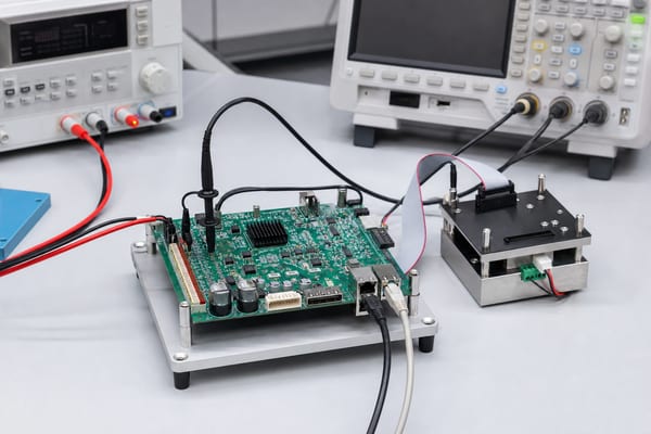
AI robotics PCB manufacturing, functional test fixture connected to a robot controller PCBA

Buyers need a test plan that connects each risk to evidence. Before ordering, engineering should define the functions and limits that matter, procurement should confirm what the supplier includes, and both teams should agree on the records delivered with the lot. “AOI and functional test included” is not enough unless the coverage and acceptance criteria are stated.

  1. Define bare-board evidence: Require electrical testing for opens and shorts and identify any stackup, dimensional, finish, impedance-coupon, or microsection records needed for acceptance. Procurement can then confirm whether those records are included in the PCB price.
  2. Set paste-control expectations: Identify packages or thermal pads that justify SPI and agree on the defects or trends that stop the line. The supplier should explain how paste results are tied to the released stencil and board revision.
  3. Approve first-article coverage: Specify the identity, polarity, orientation, placement, and visible-joint checks required before the remaining quantity is assembled. Ask for a recorded approval rather than relying on an undocumented operator check.
  4. Request hidden-joint evidence: Map BGA, LGA, QFN, and bottom-terminated pads to X-ray coverage and project acceptance criteria. A representative image is useful only when it identifies the board, package, lot, and decision basis.
  5. Choose unpowered checks: Use ICT, flying probe, or a dedicated fixture only where test access and circuit behavior support useful limits. Engineering should define which nets, values, or rail resistances can distinguish an assembly fault from normal component tolerance.
  6. Control firmware identity: Provide the approved bootloader, MCU, FPGA, or configuration package with tool settings and a version or checksum. Require the programming result to be linked to the lot or serial number when traceability matters.
  7. Define functional acceptance: State input voltage, power sequence, interfaces, loads or simulators, expected responses, and pass/fail limits. Request measured values for critical functions instead of accepting a record that only says “powered on.”
  8. Agree on failure handling: Define which test records accompany the lot and how failures, rework, and retest are logged. This prevents repeated testing from hiding intermittent faults and gives engineering data for corrective action.

Engineering can build the functional-test scope from the board’s released interfaces and system risks:

  • Power acceptance: State startup sequence, rail limits, expected current, reset behavior, and abnormal-current response at defined input conditions.
  • Communication acceptance: Name each CAN, CAN-FD, Ethernet, USB, or other interface, together with the messages, speed, termination, and error criteria to be exercised.
  • Sensor and encoder acceptance: Provide known input states or simulator signals, expected readings, range limits, and fault responses.
  • Motor-output acceptance: Define enable, direction, PWM or command response, feedback, protection behavior, and the safe load or simulator used at PCBA level.
  • Vision-interface acceptance: Define camera detection, link mode, frame transfer, and error reporting; reserve optical alignment and final image-quality acceptance for the assembled robot where appropriate.
  • Service-function acceptance: Identify programming ports, storage, GPIO, indicators, and service interfaces that must work before the PCBA is shipped.

Separate PCBA acceptance from robot-level validation. Put the boundary in the purchase specification: the supplier can release the assembled board against agreed electrical and functional limits, while motion accuracy, navigation, sustained system thermal loading, full actuator performance, optical alignment, safety behavior, and final-product EMC remain system-level responsibilities unless separately contracted.

What Common Problems Cause AI Robot PCB Prototypes to Fail?

Combined loads reveal failures missed by power-on checks. Motors, processors, sensors, cameras, and communication interfaces can create simultaneous electrical and thermal conditions that do not appear when each function is checked separately.

  • Reset during motor startup: Check rail droop, bulk capacitance, regulator response, connector resistance, and motor-current return paths.
  • Unstable sensor readings: Check sensor grounding, reference supplies, switching-node proximity, and routing near analog or encoder signals.
  • Camera or interface errors: Check impedance, pair routing, return paths, connector pinout, layer transitions, and assembly quality.
  • Processor overheating: Check package power, exposed-pad soldering, thermal vias, heat spreading, heat-sink contact, and enclosure cooling.
  • Intermittent BGA faults: Review X-ray results, reflow data, package handling, and board warpage before treating the fault as software-related.
  • Connector faults during movement: Check retention, solder support, cable strain, board flex, and enclosure interference.
  • Build-to-build inconsistency: Compare the PCB, stackup, BOM, manufacturer part numbers, firmware, assembly files, and test procedure by revision.

Convert an effective prototype rework into an approved design or process change before the next build.

How Do You Move an AI Robotics PCB from Prototype to Mass Production?

Engineering and procurement should release one production baseline. A working prototype is not enough for a repeat order. The purchase package must connect approved design data, components, firmware, inspection, test limits, deviations, and commercial scope to one revision.

Use the following customer-side release checklist before authorizing volume production:

  1. Approve one PCB baseline: Release the PCB revision, stackup, Gerber/ODB++, drill data, fabrication drawing, and impedance requirements together. Put the same revision identifier on the purchase order and supplier acknowledgement.
  2. Close DFM questions: Assign an owner and disposition to BGA breakout, microvia, current-path, panel, clearance, paste, and mechanical issues before approving tooling or a stencil.
  3. Approve the production BOM: Confirm manufacturer part numbers, allowed alternatives, do-not-substitute items, moisture sensitivity, and programming requirements. Procurement should not accept a substitution until engineering evaluates its electrical, thermal, mechanical, firmware, and qualification effects.
  4. Match assembly files: Check that the BOM, CPL, assembly drawings, polarity data, special-process notes, and board data belong to the same release. Send one controlled package rather than separate email attachments with uncertain revisions.
  5. Agree on process evidence: Confirm which SPI, first-article, AOI, X-ray, soldering, and workmanship records the supplier will create and which records the customer will receive or may review.
  6. Release programming files: Provide firmware, bootloader, configuration, tool settings, and the required version or checksum record. State whether traceability is by lot, panel, or individual serial number.
  7. Set acceptance limits: Define the defects and limits covered by visual inspection, AOI, X-ray, electrical checks, and functional testing. Do not leave acceptance to an unspecified factory default.
  8. Approve the test package: Release power limits, sequencing, interfaces, loads, fixtures, software, expected responses, and pass/fail criteria. Where practical, challenge the station with known-good and known-fault conditions before relying on its results.
  9. Review the pilot build: Compare the intended materials, programs, tooling, inspection, and test flow with what was actually used. Close deviations, rework trends, and test escapes through documented actions.
  10. Authorize volume release: Approve the updated package only after pilot findings are closed and the accepted first-article and test evidence represent the intended production configuration.

During pilot review, check paste variation, fixture access, connector insertion, thermal-pad consistency, rework trends, and test cycle practicality. Repeat orders should reference the approved baseline and require disclosure of material, component, process, firmware, or test changes.

What Should You Look for in an AI Robotics PCB Manufacturer and Assembly Partner?

Choose a partner by risk closure and evidence. An AI robotics PCB manufacturer should connect bare-board fabrication, component sourcing, assembly, programming, inspection, and test to the customer’s released requirements rather than quote each operation in isolation.

Before placing an order, compare suppliers on these customer-facing commitments:

  • Reviewed manufacturing proposal: Request a stackup, via structure, copper construction, panel approach, and DFM response tied to the actual design.
  • Comparable quotation scope: Confirm whether tooling, stencil, component sourcing, programming, SPI, AOI, X-ray, electrical test, functional test, packaging, and records are included or excluded.
  • Controlled component sourcing: Require purchasing by manufacturer part number and written approval before any alternative is used.
  • Package-specific inspection: Map fine-pitch and hidden-joint packages to the inspection method and acceptance criteria that will be applied.
  • Programming traceability: Agree on firmware identity, programming records, and the lot-level or serial-level traceability needed by the project.
  • Pilot-to-volume continuity: Confirm how approved materials, programs, tooling, deviations, and test limits will carry from prototypes into repeat orders.
  • Failure and change disclosure: Define how nonconforming results, rework, substitutions, and process changes will be reported before shipment or reuse.

A supplier response that names these deliverables gives engineering a technical review path and gives procurement a comparable commercial baseline. If the quotation leaves them undefined, later tooling, sourcing, inspection, or acceptance changes can create avoidable cost and schedule risk.

Why Choose EBest Circuit for AI Robotics PCB Manufacturing and Assembly?

One controlled project package reduces manufacturing handoffs. EBest Circuit coordinates fabrication, sourcing, assembly, inspection, and test preparation, giving engineering and purchasing teams one manufacturing contact from prototype verification through repeat production.

  • Free DFM review: Identify stackup, via, footprint, panel, and assembly conflicts before tooling, reducing avoidable prototype rework.
  • Prototype-to-production continuity: Keep approved PCB data, BOM revisions, assembly programs, and inspection requirements aligned as volumes increase.
  • HDI and fine-pitch support: Match BGA breakout, via-in-pad, controlled impedance, and assembly controls to the released design instead of applying unnecessary complexity.
  • Component sourcing control: Purchase against manufacturer part numbers and approved alternatives, helping prevent unapproved substitutions and BOM drift.
  • Inspection matched to package risk: Combine bare-board electrical test, SPI, AOI, and X-ray where each method can detect the relevant defect class.
  • Programming and functional-test support: Build around your controlled firmware, procedures, fixtures, and pass/fail limits so delivered evidence matches your acceptance plan.

What Files Are Needed for an AI Robotics PCB and PCBA Quote?

A quotation must define the complete manufacturing scope. PCB construction, component sourcing, assembly work, programming, and testing affect the manufacturing route. Missing inputs can make the initial price incomplete.

For AI robotics PCB manufacturing, provide:

  • PCB image data: Gerber or ODB++ files.
  • Drill data: NC drill files.
  • Fabrication drawing: PCB fabrication drawing.
  • Stackup definition: Defined stackup, if available.
  • Impedance specification: Controlled-impedance requirements.
  • Copper specification: Copper requirements.
  • Surface finish: Surface finish.
  • Order quantity: Order quantity.
  • Special structures: Special via or mechanical requirements.

For AI robotics PCB assembly, also provide:

  • Production BOM: BOM with manufacturer part numbers.
  • Placement data: CPL or Pick-and-Place file.
  • Assembly drawing: Assembly drawing.
  • Component alternatives: Approved component alternatives.
  • Programming package: Firmware or programming files when required.
  • Functional-test procedure: Functional-test procedure.
  • Test fixture: Test fixture information, if available.
  • Protective materials: Conformal-coating or underfill requirements when specified.
  • Packaging and labeling: Packaging and labeling requirements.

Gerber files do not define sourcing, placement, programming, or functional testing. Send the available package so missing quotation inputs can be identified before order release.

FAQs About AI Robotics PCB Manufacturing and Assembly

Q1: Can an AI robotics PCBA combine SMT, through-hole, and press-fit components?
A1: Yes. Mixed assembly can combine SMT devices, through-hole connectors, and press-fit components when the PCB hole tolerances, assembly sequence, and mechanical requirements are defined before production.

Q2: How should irregular robot PCBs be panelized for assembly?
A2: Panelization should provide enough support for printing, placement, reflow, inspection, and depanelization. Irregular outlines may require breakaway rails, routing tabs, or dedicated tooling so the PCB remains stable during SMT production.

Q3: Can customer-supplied AI processors or computing modules be used for assembly?
A3: Yes. Consigned components can be used when the component identity and handling condition are confirmed against the BOM, supplied quantity, packaging, and moisture status before assembly.

Q4: How are ESD-sensitive sensors and processors handled during PCBA production?
A4: ESD-sensitive parts should remain within an ESD-controlled handling process, including suitable workstations, storage, transport, grounding, and packaging according to the component requirements.

Q5: Can serial numbers or QR codes be added to robotics PCB assemblies?
A5: Yes. Serial numbers, labels, or QR codes can be linked to production lots, PCB revisions, assembly records, or test results when traceability is required.

Q6: How should board-to-board and cable connectors be selected for repeated mating cycles?
A6: Connector selection should verify mating life, retention, electrical load, and mechanical fit against the expected vibration, signal speed, cable strain, and available installation space. The PCB footprint alone does not determine connector suitability.

Q7: Can robotics PCBA production use lead-free soldering?
A7: Yes. Lead-free assembly is widely used when the PCB finish, components, solder alloy, and reflow profile are compatible with the required process.

Q8: How should assembled AI robotics PCBs be packed before shipment?
A8: Packaging should control ESD, mechanical, contamination, and moisture risks. The selected tray, bag, cushioning, and outer carton should match component sensitivity, connector exposure, board size, and shipment conditions.

Q9: What information is needed to quote a functional test?
A9: Provide the test conditions, interfaces, limits, and fixture status, together with the applicable software or scripts and expected responses. If the fixture is not yet available, identify which checks belong to PCBA production and which remain at final robot integration.

Q10: When should a pilot build be repeated before mass production?
A10: Repeat the pilot after a released design, process, firmware, test, or interface change whenever the existing build evidence no longer represents the intended production configuration.

Conclusion

Repeatability depends on one approved baseline. Keep PCB construction, components, assembly, firmware, inspection, and test limits aligned across repeat orders.

EBest Circuit can review your AI robotics PCB manufacturing package from prototype planning through repeat production. Submit the released manufacturing package: Gerber/ODB++, BOM, CPL, assembly drawing, quantity, programming package, and applicable test requirements. Email sales@bestpcbs.com for a free DFM review and quotation.

You may also like

Robotics PCB Manufacturer
Thursday, June 11th, 2026

Is your robotics PCB still stable after motor startup, sensor feedback and real motion testing? Many robotics PCB problems do not appear during basic power-on checks. They usually appear when the motor starts, the sensor begins sending feedback, or the robot runs under vibration and heat. At that stage, voltage drop, signal noise, AI module heating and weak connector soldering can delay the whole project.

EBest is a China source factory for robotics PCB manufacturing, PCB assembly, component sourcing and testing. Founded in 2006, EBest supports motion control PCB, sensor PCB, robot power PCB and AI module PCB from prototype to mass production, helping robot projects move from early validation to stable batch production.

What Robotics PCB Problems Can EBest Help You Prevent?

EBest helps prevent unstable power, motor interference, sensor errors, AI module heating, solder joint failure and inconsistent batch quality before delivery. These issues often appear after basic power-on testing, especially when the robot starts moving under real motor load and vibration.

Common robotics PCB risks include:

  • Motor startup voltage drop that causes random reset
  • Sensor noise that affects detection and feedback
  • AI module heating that reduces long-term reliability
  • Weak connector soldering that fails under movement
  • Poor assembly consistency between prototype and batch production
  • Component sourcing delay before mass production
  • Insufficient testing before final delivery

A robotics PCB manufacturer should not only fabricate the board. It should review production risks, control soldering quality, check component availability and support testing before delivery.

How Does EBest Support Robotics PCB Manufacturing?

EBest supports robotics PCB manufacturing through PCB design, PCB prototype, mass production, component sourcing, PCB assembly, inspection and testing. This keeps production review, parts preparation, assembly and delivery in one controlled process.

  • PCB design and production review
    EBest can review Gerber files, BOM, pick-and-place files and assembly drawings before production. This helps check power areas, component spacing, connector positions, test points and assembly risks before the robotics PCB enters fabrication.
  • PCB prototype for early robot testing
    Prototype service helps verify motion control, sensor feedback, robot power PCB stability and AI module function before batch production. Early sample testing can expose voltage drop, signal noise, heat issues or connector risks before the project moves forward.
  • Component sourcing for BOM control
    EBest reviews component availability, package type, lead time and sourcing risk before assembly. This is important for robotics PCB projects that use motor drivers, sensors, wireless modules, AI processors, connectors and high-current power components.
  • PCB assembly for robot applications
    EBest supports SMT assembly, THT assembly and mixed assembly for robotics PCB projects. This fits boards that combine compact ICs, sensors, connectors, terminals, motor driver circuits and power components on one PCBA.
  • Mass production for repeat orders
    After prototype validation, EBest can support small batch, mid-volume robotics PCB assembly and high-volume robotics PCB assembly. Controlled assembly and inspection help keep board quality more consistent across repeat orders.
  • Inspection and testing before delivery
    EBest can support AOI inspection, X-ray inspection, electrical testing, power-on testing and functional testing based on project requirements. For robot PCB assembly service, testing should confirm power, signal, communication and key module functions before shipment.

This service flow helps robotics PCB projects move from design files to assembled boards with clearer production control, fewer supplier handoffs and better preparation before batch delivery.

Which Robotics PCB Applications Can EBest Build?

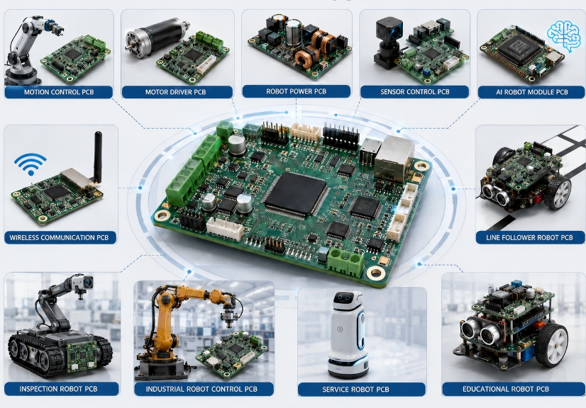
EBest can manufacture and assemble robotics PCBs for motion control, motor drivers, sensor systems, power boards, AI modules, wireless communication and automation equipment. This allows one supplier to support several board types within the same robot project.

Typical robotics PCB applications include:

  • Motion control PCB
  • Motor driver PCB
  • Robot power PCB
  • Sensor control PCB
  • AI robot module PCB
  • AI robotics PCB manufacturing
  • Wireless communication PCB
  • Line follower robot PCB
  • Line following robot PCB
  • Inspection robot PCB
  • Industrial robot control PCB
  • Service robot PCB
  • Educational robot PCB

These boards often combine power, signal, communication and mechanical stress. As a result, PCB quality, component placement and inspection control directly affect robot operation.

Robotics PCB Applications

How Does PCB Quality Affect Robot Motion Accuracy?

PCB quality affects robot motion accuracy through power stability, motor driver performance, encoder signal quality, EMI control and assembly consistency. If the motor driver cannot receive stable current, the robot may move with delay, drift or random stop.

Motion control PCB projects usually include drivers, controllers, encoders, connectors and power circuits. When motor EMI affects encoder or control signals, the robot may move incorrectly even when the software logic is right.

For this reason, robotics PCB design should review power trace width, grounding, EMI separation, connector strength and test points before production. During assembly, accurate placement and strong solder joints help keep batch robots performing consistently.

Key review points include:

  • Motor control voltage: commonly 5V-48V
  • Control signal level: commonly 1.8V-5V
  • Encoder signal type: digital or analog
  • PCB copper weight: commonly 1oz-3oz
  • Test point spacing: commonly 1.0mm-2.54mm

How Do Sensor PCBs Improve Signal Stability in Robots?

Sensor PCBs improve signal stability by supporting clean grounding, low-noise routing, accurate component placement and reliable connector assembly. Stable sensor input helps robots detect objects, follow paths, avoid obstacles and control movement feedback.

In a line follower robot PCB, unstable sensor signals may cause the robot to drift, stop or misread the path. In inspection robots, poor signal quality may affect detection accuracy and response time.

Therefore, sensor PCB production should focus on grounding, connector quality, component polarity and signal integrity. EBest supports PCB in robotics applications where sensor stability must be checked together with assembly quality and testing requirements.

What Makes AI Robotics PCB Assembly More Challenging?

AI robotics PCB assembly is more challenging because AI modules often require stable power, thermal control, high-density SMT placement, camera interfaces and multi-sensor connections. The main risks are high current load, heat concentration, signal interference and hidden soldering defects.

AI robot power PCB projects may place processors, memory, wireless modules, sensors and power circuits in a compact area. If the assembly process is not controlled, BGA, QFN or small-pitch components may create hidden soldering defects.

AI robot testing PCB requirements should go beyond simple power-on checks. The test should confirm power stability, communication, sensor interface, camera connection and module operation before delivery to improve AI robot PCB reliability.

Robotics PCB Assembly

What Should Be Reviewed Before Robotics PCB Production?

Power layout, grounding, EMI control, thermal design, connector placement, component spacing, test points and BOM availability should be reviewed before robotics PCB production. This helps reduce rework before PCB fabrication and assembly begin.

A practical robotics PCB production review should check whether high-current areas are wide enough, whether sensor signals are protected from motor noise, and whether connectors can handle movement and vibration.

BOM review is also important. If key components are obsolete, out of stock or difficult to source, the project may face delay before batch assembly. EBest reviews these risks early so customers can adjust before production.

Production review should cover:

  • Power trace width for current capacity and heat control
  • Grounding design for signal and power return paths
  • EMI control for motor and switching noise reduction
  • Thermal layout for drivers, regulators and AI modules
  • Connector position for vibration-sensitive areas
  • Component spacing for SMT assembly clearance
  • Test point access for production testing
  • BOM availability for sourcing and lead time control

How Does PCB Assembly Quality Reduce Robotics PCB Failure Risk?

PCB assembly quality reduces robotics PCB failure risk by improving solder joint strength, connector reliability, component placement accuracy and inspection consistency. This is important for robot boards that work under movement, vibration, heat and repeated load changes.

Cold solder joints, insufficient solder, wrong polarity and shifted components may pass simple power-on checks. However, they can cause random failure during long-term robot operation or during system-level testing.

For robotics PCB assembly, SMT precision matters for ICs, sensors and communication modules. THT quality matters for terminals, connectors and power parts. Mixed assembly is useful when one robot board combines compact SMT devices with high-current components.

Assembly risk points include:

  • Cold solder joints that cause intermittent failure
  • Insufficient solder on high-current pads
  • Wrong polarity components that damage power circuits
  • Connector solder cracks under vibration
  • Shifted components that affect signal or power paths
  • Flux residue that may affect long-term reliability
  • Batch inconsistency between prototype and repeat orders

What Tests Are Needed Before Robotics PCB Delivery?

AOI, X-ray inspection, electrical testing, functional testing, power-on testing, thermal review and customized reliability testing may be required before robotics PCB delivery. The final test plan should match the robot’s working environment and board function.

Common robotics PCB tests include:

  • AOI inspection for SMT placement and soldering quality
  • X-ray inspection for BGA, QFN and hidden solder joints
  • Electrical test for open and short circuit checking
  • Functional test for power, signal and communication
  • Power-on test for basic operating confirmation
  • Thermal review for motor drivers, regulators and AI modules
  • Connector inspection for vibration-sensitive applications
  • Custom robot PCB reliability test based on project requirements

These tests help reduce delivery risk before the robot enters full system testing. For AI robot testing PCB projects, power, signal and communication checks should be confirmed before shipment.

Case Study: Reducing Motion and Sensor Issues Before Batch Production

A robotics PCB project can pass basic power-on testing but still fail during real movement if motor load, sensor noise, vibration and soldering quality are not controlled before batch production. This case shows how production review helps reduce motion and sensor risks before mid-volume assembly.

Project Background

The customer was developing a mobile robot control board for motor control, sensor feedback and power distribution. The prototype could power on, but the board reset when the motor started. During movement testing, the sensor signal also became unstable, which affected motion accuracy and feedback reliability.

Customer Requirements

The project required stable power delivery, lower motor interference, stronger connector soldering, cleaner sensor feedback and consistent PCB assembly quality. The customer also wanted to reduce repeated prototype rework before moving to batch production.

Our Solution

EBest reviewed the Gerber files, BOM, assembly drawing and testing requirements before production. Our team checked high-current power areas, grounding paths, connector positions, component sourcing risks and assembly feasibility. During production, EBest controlled SMT placement, THT soldering, connector assembly, inspection and functional testing.

Output Result

The project moved from prototype validation to mid-volume robotics PCB assembly with lower production risk. The board showed lower reset risk during motor startup, more stable sensor feedback during movement and better consistency before robot system-level testing.

Key results included:

  • Lower motion failure risk during motor startup
  • More stable sensor feedback during robot movement
  • Stronger connector soldering for vibration-sensitive areas
  • Better batch consistency before mid-volume production
  • Less rework before final robot system testing
  • Faster transition from prototype validation to batch assembly

Why Choose EBest for Robotics PCB Manufacturing?

EBest provides PCB fabrication, component sourcing, PCB assembly, testing support and batch production service from one China source factory. For robotics PCB projects, this helps reduce supplier handoff, shorten communication time and lower production risk before delivery.

  • One-stop PCB and PCBA service
    EBest supports PCB design, PCB prototype, mass production, component sourcing and PCB assembly in one service flow. This keeps board production, parts sourcing and assembly communication in the same production chain.
  • 20+ years of PCB manufacturing experience
    Founded on June 28, 2006, EBest Circuit, also known as Best Technology, has over 20 years of PCB manufacturing experience. This supports robotics PCB production review from prototype verification to stable batch production.
  • Monthly production capability
    EBest’s monthly production capability reaches 260,000 square feet / 28,900 square meters, with more than 1,000 different boards completed monthly. This capacity supports prototype runs, repeat orders, mid-volume robotics PCB assembly and high-volume robotics PCB assembly.
  • Expedited service for urgent boards
    For urgent boards, EBest can provide expedited service, and eligible urgent boards can be shipped within 24 hours when project files, materials and production conditions allow. This is suitable for robotics PCB prototype verification and pilot production schedules.
  • Wide robotics PCB structure support
    EBest supports FR4 PCB, multi-layer PCB, Metal Core PCB, Ceramic PCB, flexible PCB, rigid-flex PCB, RF PCB, High Tg PCB, heavy copper PCB, HDI PCB, high-speed PCB, impedance control PCB and busbar PCB. These options fit robot power PCB, sensor PCB, motion control PCB and AI module PCB requirements.
  • SMT, THT and mixed assembly capability
    EBest supports SMT assembly, THT assembly and mixed assembly for robotics PCB projects. This is important for boards that combine compact ICs, sensors, connectors, terminals and high-current power components.
  • Certified quality and compliance systems
    EBest holds IATF 16949, ISO 9001:2015, ISO 13485:2016, AS9100D, REACH, RoHS and UL. These certifications support process control, material compliance and quality management for global B2B applications.
  • China source factory with global delivery
    EBest does not claim overseas factories, overseas warehouses or local branches. The service is based on China source-factory manufacturing, component sourcing, PCB assembly and global delivery support.

For robotics PCB assembly, EBest supports motion accuracy, sensor stability, AI robot PCB reliability and batch delivery through controlled manufacturing, assembly and testing.

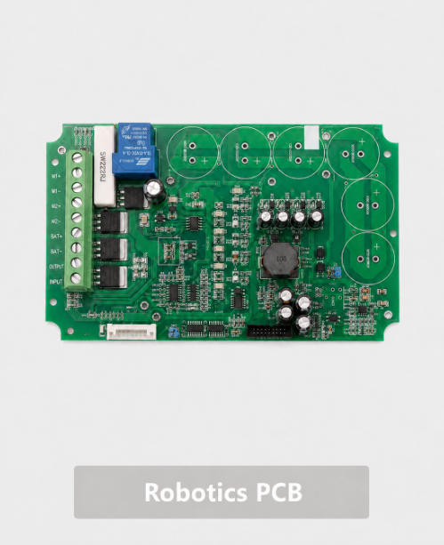
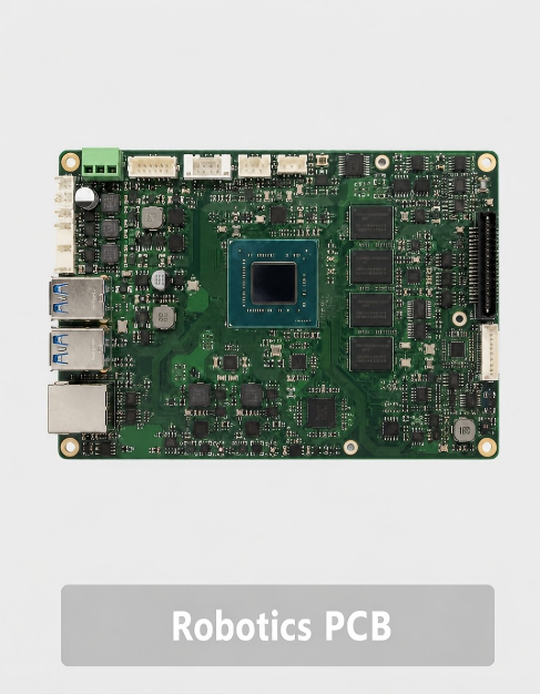
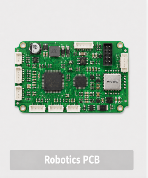
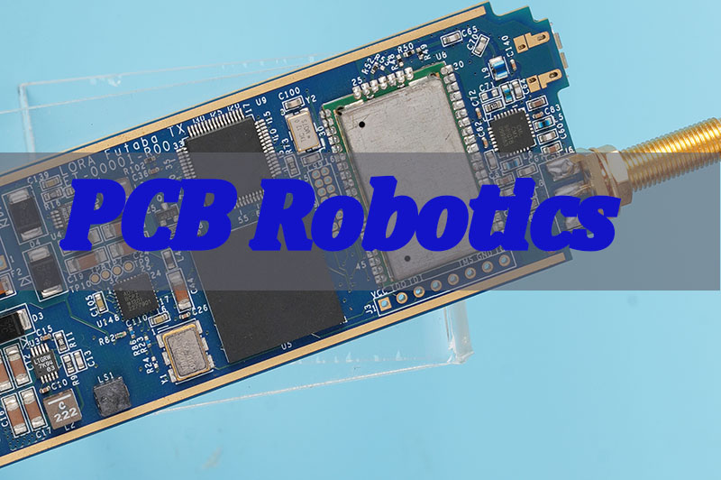
Robotics PCB

What Files Should You Send for a Robotics PCB Quote?

Send Gerber files, BOM, pick-and-place file, assembly drawing, quantity, testing requirements and special notes about motor load, vibration, heat or working environment for a robotics PCB quote. Complete files help EBest review cost, lead time and production feasibility faster.

Recommended quote files include:

  • Gerber file in RS-274X format
  • BOM in XLS, XLSX or CSV format
  • Pick-and-place file in CSV or TXT format
  • Assembly drawing in PDF format
  • PCB stack-up if required
  • Surface finish requirement
  • Order quantity in units or panels
  • Testing requirement in PDF or TXT format
  • Special notes for motor load, vibration, heat or working environment

If the project includes AI modules, high-current motor drivers or critical sensors, share the test method and operating condition early. This allows a more accurate production review and reduces repeated confirmation before quotation.

FAQs About Robotics PCB Manufacturing

Q1: What is the MOQ for robotics PCB assembly?
A1: The MOQ depends on PCB complexity, component sourcing and testing requirements. For prototype projects, EBest can support small trial orders. For repeat production, mid-volume or high-volume robotics PCB assembly is more suitable after the design, BOM and test process are stable.

Q2: Can EBest source components for robotics PCB assembly?
A2: Yes. EBest can support component sourcing based on the customer’s BOM. Before assembly, the team can review part numbers, package types, availability and lead time risks. For motor drivers, sensors, connectors and AI modules, early BOM review helps reduce production delay.

Q3: What affects the cost of a robotics PCB project?
A3: The main cost factors include PCB layer count, board size, copper weight, surface finish, component quantity, package difficulty, assembly type, testing scope and order volume. BGA, QFN, fine-pitch parts, high-current areas and functional testing can increase the total project cost.

Q4: Should I send a test fixture for robotics PCB functional testing?
A4: If the board requires motion control, sensor feedback, communication or AI module verification, a test fixture is recommended. A fixture helps confirm power, signal and interface functions more consistently before shipment, especially for batch robotics PCB assembly and repeat orders.

Q5: Can EBest handle alternative components if some parts are out of stock?
A5: EBest can help review possible alternative components, but final approval should come from the customer. For robotics PCB projects, replacement parts must match package size, electrical rating, tolerance, temperature range and functional requirements before they are used in production.

Q6: What files are required for faster robotics PCB quotation?
A6: For faster quotation, send Gerber files, BOM, pick-and-place file, assembly drawing, quantity and testing requirements. If the robotics PCB includes motor drivers, sensors, AI modules or high-current circuits, include operating conditions and special inspection notes early.

Q7: Can EBest support both prototype and batch robotics PCB production?
A7: Yes. EBest supports PCB prototype, small batch, mid-volume and high-volume robotics PCB assembly. Prototype production is used for function verification, while batch production focuses on assembly repeatability, inspection control, component supply and delivery consistency.

Q8: What should be confirmed before moving from prototype to batch production?
A8: Before batch production, confirm circuit function, BOM stability, test method, component availability, connector strength, thermal performance and assembly process. For robotics PCB projects, motor load, sensor stability and AI module power behavior should be checked before scaling.

Q9: Can EBest assemble robotics PCBs with both SMT and THT parts?
A9: Yes. EBest supports SMT, THT and mixed assembly. This is useful for robotics PCB projects that combine small ICs, sensors, wireless modules, connectors, terminals and high-current power components on the same board.

Q10: What surface finish is suitable for robotics PCB manufacturing?
A10: Common surface finishes include HASL, lead-free HASL, ENIG and OSP. The right choice depends on component package, soldering requirement, shelf life, cost and reliability needs. For fine-pitch components, BGA or AI module boards, ENIG is often considered during production review.

Q11: How can robotics PCB batch consistency be improved?
A11: Batch consistency can be improved through stable BOM control, clear assembly drawings, approved process settings, AOI inspection, soldering control, functional testing and consistent packaging. For robotics PCB assembly, repeatable production control is important because small defects may affect robot movement or sensor feedback.

Q12: Can EBest support urgent robotics PCB prototype orders?
A12: EBest can provide expedited service for urgent boards when project files, materials and production conditions allow. Eligible urgent boards can be shipped within 24 hours. For faster handling, customers should provide Gerber files, BOM, quantity and assembly requirements at the beginning.

Q13: What certifications does EBest have for PCB manufacturing?
A13: EBest holds IATF 16949, ISO 9001:2015, ISO 13485:2016, AS9100D, REACH, RoHS and UL. These systems support process control, quality management and compliance needs for global B2B PCB projects, including robotics PCB manufacturing and assembly.

Q14: Can a China source factory support overseas robotics PCB projects?
A14: Yes. A China source factory can support overseas robotics PCB projects through custom manufacturing, component sourcing, PCB assembly, testing and global delivery. EBest does not claim overseas factories, overseas warehouses or local branches. The service is based on China source-factory production.

Get a Robotics PCB Quote for Your Project

A reliable robotics PCB should support stable motion, clean sensor feedback, controlled power delivery and tested assembly quality before it enters real robot operation. For motion control boards, sensor boards, AI robot modules and robot power PCB projects, early production review can reduce rework, prevent batch inconsistency and lower delivery risk.
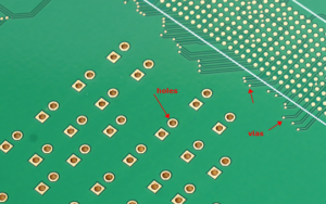
For selection, choose a robotics PCB manufacturer that can review design files, source components, assemble SMT and THT parts, inspect solder quality and support functional testing. For procurement, prepare complete Gerber files, BOM, pick-and-place files, quantity and test requirements before requesting a quote.

EBest Circuit is a China source factory supporting robotics PCB manufacturing and assembly, component sourcing, testing and global delivery for robot projects. Send your Gerber files, BOM, quantity and testing requirements to sales@bestpcbs.com for a robotics PCB manufacturing and assembly quote.

You may also like

Robotics PCB Manufacturing | 1.5-Week PCBA Turnaround
Monday, March 2nd, 2026

Robotics PCB determines whether a robot moves with precision or drifts under load, whether sensor data remains stable or becomes distorted by noise, and whether the system survives real-world vibration and thermal cycling. In industrial and AI-driven robotics platforms, PCB design and manufacturing discipline are often the deciding factors between scalable deployment and repeated field failure.

From a customer perspective, robotics projects frequently encounter structural bottlenecks during transition from prototype to production:

  • Motion instability under dynamic load
  • Sensor interference caused by EMI and poor grounding
  • Overheating inside compact enclosures
  • Low first-pass yield during pilot runs
  • Difficulty scaling from small batch to high volume

From a manufacturing engineering perspective, these issues are preventable when addressed early:

  • Optimized high-current routing and isolated signal layers
  • Stack-up planning to separate power and logic domains
  • Thermal vias and copper balancing for heat dissipation
  • DFM review before SMT release to improve yield
  • Flexible production strategy for smooth scale-up

EBest Circuit (Best Technology) approaches robotics control PCB and PCBA projects from an engineering-first standpoint. We support robotics PCB design review, motor controller boards, AI-enabled control modules, and mixed-signal robotic systems with in-house fabrication and SMT capability. Our experience spans prototype builds to scalable production, ensuring process stability and long-term reliability. For robotics PCB manufacturing and assembly support, pls feel free to contact us via sales@bestpcbs.com.

Robotics PCB

What Defines a Reliable Robotics PCB in Industrial Automation Applications?

A reliable robotics PCB must operate stably under vibration, current surges, EMI exposure, and temperature fluctuation. It is engineered with margin, not just minimum compliance.
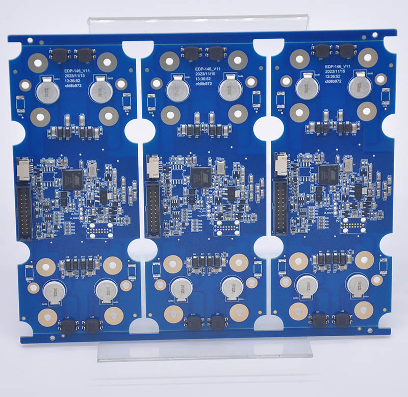
In real automation environments, robots run continuously under load. Minor grounding flaws or insufficient copper thickness can introduce cumulative instability. Over time, this leads to encoder drift, communication jitter, or unpredictable resets.

On the shop floor, we often see failures originating from copper imbalance during lamination or insufficient via reinforcement near motor connectors. These weaknesses may pass functional tests but fail during extended runtime.

Key technical considerations include:

  • Segregation of motor drive and logic layers
  • Controlled impedance routing for communication buses
  • Reinforced mounting hole structures
  • Thermal management through copper balancing
  • EMI shielding and ground plane integrity

From an engineering perspective, structural reliability must be established before refining performance parameters.

How Does Robotics PCB Design Affect Robot Stability and Motion Accuracy?

Robotics PCB design directly influences servo loop response, sensor accuracy, and communication timing. Layout errors introduce micro-noise that propagates through control algorithms.

When designing motor control and encoder circuits, trace length and return path consistency are critical. Poor placement of gate drivers or high-current traces near analog inputs introduces noise coupling.

In production builds, improper decoupling capacitor placement results in voltage ripple under dynamic torque. Firmware compensation cannot fully correct hardware-level layout mistakes.

Critical layout factors include:

  • Short and symmetrical return paths
  • Differential pair matching for fieldbus communication
  • Proper decoupling capacitor proximity
  • Dedicated analog ground reference
  • Copper thickness selection for motor zones

With this in mind, assembly precision becomes equally decisive in maintaining system integrity.

Why Is Robotics PCB Assembly Different from Standard PCBA Projects?

Robotics PCB assembly combines high-current power stages, fine-pitch processors, and often HDI or rigid-flex structures within a single board. The manufacturing tolerance window is narrower than consumer electronics.

Motor drivers generate localized heat, while processors demand precise reflow control. Voiding beneath thermal pads or uneven solder distribution can compromise performance.

In practice, insufficient stencil optimization leads to poor thermal contact for MOSFETs. Over time, this increases junction temperature and accelerates failure.

Key assembly control points include:

  • Stencil aperture tuning for power devices
  • X-ray inspection of BGA and thermal pads
  • Controlled reflow profiling
  • Selective soldering for through-hole connectors
  • AOI calibration for mixed-package boards

That said, AI-enabled robotics introduces even greater density and thermal complexity.

When Should You Choose AI Robot PCB Assembly for Advanced Control Systems?

AI robot PCB assembly is required when edge computing, multi-sensor fusion, and high-speed memory routing demand HDI-level precision.
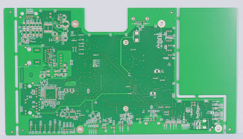
AI processors require stable, low-noise power rails and controlled impedance routing. Assembly quality directly affects long-term BGA reliability.

In manufacturing, inadequate temperature profiling during reflow can create hidden micro-cracks beneath AI processors. These issues often emerge only after thermal cycling in the field.

Key implementation factors include:

  • HDI microvia integrity verification
  • Controlled impedance stack modeling
  • Thermal pad solder quality control
  • Memory routing length matching
  • Power plane segmentation

As a result, fabrication capability must align with AI-driven system demands.

How Does Robot Control PCB Manufacturing Impact System-Level Reliability?

Robot control PCB manufacturing determines mechanical durability and long-term electrical stability. Material selection and plating quality influence lifecycle performance.

Boards exposed to repetitive heating cycles must maintain via integrity and laminate adhesion. Low Tg materials or insufficient copper plating can lead to delamination.
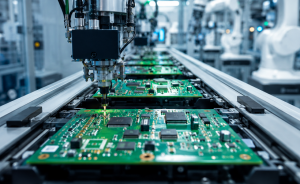

In field returns, common failure modes include cracked vias near motor connectors and solder fatigue in high-current zones.

Manufacturing-critical elements include:

  • High Tg laminate selection
  • Adequate via barrel thickness
  • Symmetrical copper distribution
  • Surface finish consistency
  • Controlled board flatness

More importantly, power architecture design plays a decisive role in overall system robustness.

What Power Architecture Considerations Matter Most in Robot Power PCB?

Robot power PCB design must support surge current, battery fluctuations, and regenerative braking without voltage instability.

If power routing is undersized, torque peaks cause voltage drop and MCU resets. This creates unpredictable system behavior.

During SMT production, thin copper traces and insufficient thermal relief often become failure hotspots under load testing.

Power design essentials include:

  • 2–6 oz copper thickness selection
  • Short high-current loops
  • Optimized MOSFET pad geometry
  • Thermal via arrays beneath power devices
  • Robust decoupling capacitor networks

At this stage, high-density routing considerations often emerge in advanced robotics systems.

How Do AI Robot HDI PCB Requirements Change Stack-Up and Layout Strategy?

AI robot HDI PCB structures enable compact designs and high-speed signal routing but demand precise stack-up planning.

Sequential lamination and microvia structures allow dense routing but increase fabrication complexity. Poor stack symmetry introduces warpage during reflow.

On the production line, improper resin flow control during lamination can reduce microvia reliability, impacting long-term signal integrity.

Design and fabrication factors include:

  • Sequential lamination planning
  • Controlled impedance modeling
  • Laser microvia inspection
  • Resin flow management
  • Stack symmetry optimization

Ultimately, verification testing validates whether design and manufacturing choices meet field demands.

What Testing Standards Are Required for Robotic PCB Testing in Harsh Environments?

Robotic PCB testing must simulate electrical, thermal, and mechanical stress conditions that mirror real deployment.

Industrial robots face vibration, dust, and temperature variation. Basic ICT alone cannot guarantee durability.

In manufacturing practice, burn-in testing and dynamic load simulation reveal marginal boards before shipment.

Testing protocol essentials include:

  • ICT and FCT validation
  • Thermal cycling testing
  • Vibration simulation
  • Power load stress testing
  • Extended burn-in procedures

All things considered, scalable production capability determines whether robotics projects grow successfully.

How to Select a Robotics PCB Assembly Partner for Scalable Production?

Selecting a robotics PCB assembly partner requires evaluating engineering depth, SMT capability, and scalability planning.

A factory experienced in robotics understands mixed-signal motor control boards and AI processor integration. Without that experience, yield instability becomes common during scale-up.

In real production transitions, lack of DFM feedback and process control often causes yield drops when moving from pilot to mass production.

Key evaluation criteria include:

  • Proven robotics project experience
  • HDI and heavy copper fabrication capability
  • In-house SMT and inspection systems
  • Structured DFM review process
  • Flexible volume scaling capacity

Fundamentally, PCB robotics manufacturing success depends on engineering alignment from design to volume production.

Robotics PCB

To sum up, robotics pcb is the foundation of motion precision, electrical stability, and system reliability in modern automation. Engineering-led design and disciplined manufacturing prevent hidden risks before deployment. Scalable robotics PCB assembly ensures smooth transition from prototype to production.
For robotics PCB manufacturing and assembly support, pls feel free to contact us via sales@bestpcbs.com.

FAQs About Robotics PCB

What copper thickness is typical for robotics motor control PCB?

  • Motor control zones typically use 2–4 oz copper, depending on peak current demand and thermal design.

Do robotics PCB projects always require HDI technology?

  • Not always. AI-driven and compact systems benefit from HDI, while basic motor controllers may use standard multilayer boards.

How long does robotics PCB assembly take for prototype builds?

  • Prototype lead time generally ranges from 7 to 15 days, depending on layer count, material availability, and testing requirements.

Can robotics PCB manufacturing scale from small batch to high volume?

  • Yes, provided stack-up, sourcing strategy, and SMT processes are planned for scalability from the beginning.

You may also like

PCB Robotics with Quick Mid Volume Robotics PCB Assembly​
Friday, December 12th, 2025

PCB Robotics​ refers to the specialized field of designing and manufacturing printed circuit boards that serve as the central nervous system for robotic applications, enabling precise control, sensing, and actuation. This article explores the unique demands of robotics PCB design and assembly, with a focus on achieving reliability and agility in mid-volume production runs.

What are the key pain points in sourcing robotics PCB assembly​ for mid-volume orders?

  • Prolonged Lead Times:​ Standard high-volume factories have slow setups and long minimum order quantities (MOQs), causing agonizing delays for builds of 500 to 5,000 units.
  • Inflexible Processes:​ Rigid production lines cannot accommodate frequent engineering change orders (ECOs) or component substitutions common in robotics development.
  • Inconsistent Quality at Scale:​ Transitioning from hand-assembled prototypes to automated production introduces new failure points, like weak solder joints or misaligned components, that undermine reliability.
  • High Upfront Tooling Costs:​ Traditional assembly imposes high, non-recurring engineering (NRE) and fixture costs that are prohibitive for mid-volume budgets.
  • Supply Chain Fragility:​ Managing component procurement for dozens of specialized sensors, motor drivers, and MCUs across hundreds of boards is a logistical nightmare that risks production stoppages.

Overcoming these hurdles requires a partner whose operational model is built for the dynamic nature of mid volume robotics PCB assembly. The solution is a manufacturer that combines scalable processes with the agility of a prototype shop.

  • Optimized Mid-Volume Lines:​ Utilize production lines engineered for faster changeovers and efficient runs in the 500-10,000 unit range, dramatically cutting lead times.
  • Agile, Responsive Engineering:​ Work with a partner whose engineering team actively manages ECOs and provides Design for Manufacturability (DFM)​ feedback tailored for robotic assemblies.
  • Process-Driven Quality:​ Implement robust, audited processes—like automated optical inspection (AOI) and X-ray for BGAs—that ensure consistent, high-yield results from the first batch to the last.
  • Cost-Effective Scaling:​ Leverage manufacturers that minimize upfront tooling fees and offer transparent, scalable pricing models perfect for growth-stage production.
  • Integrated Component Sourcing:​ Rely on the manufacturer’s established supply chain and procurement expertise to source, manage, and kit all necessary components, de-risking your build.

BEST Technology specializes in bridging the gap between prototype and mass production. We are experts in mid volume robotics PCB assembly, offering the perfect blend of quick-turn agility and production-ready rigor. Our streamlined processes, stringent quality controls, and dedicated engineering support are designed to transform your robotic design into a reliable, market-ready product without the traditional scale-up headaches. If you would like to visit our PCB factory, pls feel free to contact us at sales@bestpcbs.com.

PCB Robotics

What is PCB Robotics?

PCB Robotics is the convergence of printed circuit board technology and robotic systems.

It encompasses everything from the PCB design for a line follower robot​ to the complex, multi-board assemblies inside industrial arms. The PCB in robotics​ is not just a carrier for components; it is the integral platform that hosts microcontrollers, sensor interfaces, power regulation, and motor drivers, forming the essential backbone for the robot’s “brain” and “nervous system.”

Success in this field hinges on PCBs that are mechanically robust, electrically reliable, and optimized for manufacturability.

PCB Robotics

How Does PCB in Robotics Enable Precise Control, Sensing, and Motion Execution?

The PCB in robotics​ acts as the central hub that integrates all subsystems. Its design directly dictates the robot’s capability and performance.

  • Data Processing Core:​ Hosts the main CPU/MPU, running control algorithms and processing data from various sensors in real-time.
  • Sensor Fusion Platform:​ Provides clean, regulated power and precise signal conditioning circuits for a suite of sensors (LiDAR, IMUs, cameras, encoders), ensuring accurate environmental data.
  • Power Distribution & Management:​ Efficiently routes and regulates high-current power to actuators and motors while providing clean, stable low-voltage power to sensitive digital and analog components.
  • Motion Control Interface:​ Contains motor drivers (H-bridges, stepper controllers) and robust connectors that translate control signals into precise physical movement.
  • Communication Backbone:​ Implements various communication protocols (CAN, Ethernet, SPI, I2C) on the board layout to ensure fast, error-free data exchange between all subsystems.

What Are the Core Design Requirements for Reliable Robotics PCB Design?

Robotics PCB design​ must satisfy a harsher set of requirements than standard consumer electronics. Reliability under stress is paramount.

  1. Mechanical Robustness: Boards must withstand constant vibration, shock, and potential physical impact. This demands:
    • Strategic stiffener placement.
    • Reinforced mounting holes (plated or with pads).
    • Conformal coating for moisture and dust protection.
  2. Thermal Management:Motor drivers and processors generate significant heat. Designs must incorporate:
    • Thermal relief pads and adequate copper pours for heat spreading.
    • Strategic placement of thermal vias under hot components.
    • Consideration for metal-core PCBs (IMPCB) for high-power sections.
  3. Signal Integrity & EMI Control:High-speed digital signals and motor noise must not interfere with sensitive analog sensor lines.
    • Careful stack-up planning with dedicated ground planes.
    • Proper separation of analog, digital, and power sections.
    • Use of filters, ferrite beads, and strategic grounding for motor driver noise mitigation.
  4. Connector & Interface Reliability:Connectors are common failure points. Designs must specify:
    • Locking or high-retention connectors for cables.
    • Strain relief features.
    • Redundant pins for critical power connections.

How Robotics PCB Assembly Differs From Standard Electronics Manufacturing?

Robotics PCB assembly​ introduces unique challenges that go beyond populating a standard board. It requires a manufacturer that understands the functional criticality of every joint and component.

  • Mixed Technology Focus:​ Robotics boards often mix large through-hole connectors (for motors), fine-pitch BGAs (for processors), and heavy thermal mass components (like MOSFETs). The assembly process must be optimized for this mix.
  • Enhanced Inspection Requirements:​ Beyond standard AOI, robotics pcbs​ often require:
    • X-ray Inspection:​ To verify solder joints under large BGAs or hidden terminations.
    • In-Circuit Test (ICT) or Flying Probe:​ For functional validation of complex circuits.
    • Stress Testing:​ Vibration or thermal cycle testing on sample batches.
  • Component Qualification:​ Using extended temperature-range or industrial-grade components is often necessary, requiring stricter supply chain oversight from the assembler.
  • Conformal Coating:​ Applying protective conformal coating is frequently a standard requirement, adding a critical process step to the assembly line.

How PCB Design for Line Follower Robot Improves Stability and Tracking Accuracy?

A line follower robot​ is a perfect case study in how PCB design​ directly impacts core performance. An optimized board layout is crucial for stability and accurate tracking.

  • Sensor Placement & Symmetry:​ The IR or optical reflectance sensors must be placed with micron-level precision relative to each other and the board’s centerline. Any asymmetry in the PCB layout​ creates inherent tracking bias.
  • Low-Noise Analog Design:​ The sensor signals are weak and analog. The PCB design​ must:
    • Provide a clean, regulated analog power supply separate from motor noise.
    • Use short, guarded traces from sensors to the analog-to-digital converter (ADC).
    • Include proper grounding and filtering to reject electrical noise from the motors.
  • Power Delivery for Motors:​ Sudden motor loads can cause voltage sags that reset the microcontroller. The design must use wide power traces, large power planes, and strategically placed bulk capacitors near the motor drivers.
  • Center of Gravity Management:​ Component placement on the PCB robot​ itself affects its physical balance. Dense components should be centered and low to prevent tipping during sharp turns.

How to Ensure the Quality for Robot PCB Assembly?

Ensuring quality in robot PCB assembly​ is a multi-stage, proactive process.

  1. Design for Excellence (DFX) Review:A collaborative pre-production review between the designer and manufacturer to eliminate manufacturability, testability, and reliability issues before fabrication.
  2. Incoming Material Inspection:​ Verifying all components against the bill of materials (BOM) for correctness and checking for moisture sensitivity (MSL) to prevent “popcorning” during reflow.
  3. Process Control During Assembly:​ Monitoring key parameters like solder paste deposition, reflow oven temperature profiles, and placement machine accuracy in real-time.
  4. Comprehensive Post-Assembly Testing:​ A combination of tests is essential:
    • Automated Optical Inspection (AOI):​ Checks for solder bridges, component misalignment, and presence.
    • X-Ray Inspection:​ Examines hidden solder joints (BGAs, QFNs).
    • Functional Testing (FCT):​ Powers up the board and runs a test program to verify all inputs, outputs, and logic.

Case about PCB in Aero Robotics Projects by BEST Technology

This project entailed the fabrication of a sophisticated 6-layer RF PCB for a mission-critical aero robotics​ system. The board’s demanding specifications—including hybrid high-frequency materials, complex HDI via structures, and tight impedance control—were designed to ensure superior signal integrity and reliability in a challenging operational environment. The successful execution of this project highlights our capability in advanced robotics pcb assembly​ and manufacturing.

6-Layer Aero Robotics RF Board Specifications:

ItemSpecification
Laminate CombinationRogers RO4350B + Isola Astra MT77 (Hybrid Lamination)
Inner Layer Copper Thickness0.5 oz (17.5 µm)
Outer Layer Copper Thickness0.5 oz (17.5 µm)
Trace Width Tolerance±1 mil (RF traces)
Solder Mask Thickness≤ 15 µm (Green solder mask, no legend)

Why Choose BEST Technology for Mid Volume Robotics PCB Assembly?

BEST Technology is engineered to be the ideal partner for your scale-up phase. We excel at mid volume robotics PCB assembly​ by removing the traditional barriers between prototyping and mass production.

  • Agility Meets Process Rigor:​ Our production lines are configured for efficient, smaller batches (500-10,000 units) without sacrificing the disciplined processes needed for consistent quality.
  • Robotics-Specific Expertise:​ Our engineers understand the unique demands of motor control, sensor integration, and ruggedized design, providing actionable DFM feedback.
  • Integrated Supply Chain Management:​ We handle the complexity of sourcing and managing the long-tail of specialized components common in robotics BOMs.
  • Comprehensive Quality Assurance:​ From automated inspection to functional testing, we build verification steps into the process to ensure every board meets the reliability demands of a robotic application.
  • Transparent Partnership:​ We provide clear communication, predictable scheduling, and scalable pricing, making us a true extension of your development team.
PCB Robotics

All in all, PCB Robotics​ is the foundational engineering discipline that transforms conceptual robotic designs into functional, reliable machines. This guide has detailed the critical considerations in design, assembly, and testing that separate a successful robotic product from a fragile prototype.

Navigating the transition to mid volume robotics PCB assembly​ requires a partner that understands both the technical complexities and the business need for speed and flexibility. BEST Technology provides this essential partnership, combining agile manufacturing with rigorous quality control to deliver robust, production-ready assemblies that accelerate your path to market. Pls contact us to discuss your project via sales@bestpcbs.com.

You may also like