A PCB thermal hotspot map helps show where heat gathers on a PCB and why that area may become risky during operation. It is used to read temperature patterns, locate overheating parts, compare test results, and decide whether the layout, copper area, vias, or material should be changed.
The map should never be judged by color alone. The real value is the link between temperature, load, airflow, stackup, component rating, and PCB design margin. This guide explains how to read, find, and reduce PCB hotspots in a practical way.
What Is a PCB Thermal Hotspot Map?
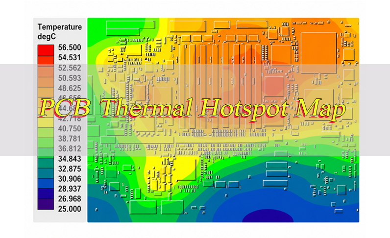
A PCB thermal hotspot map is a visual temperature image that shows where heat is concentrated on a PCB. It may come from infrared thermal imaging, thermal simulation, thermocouples, or a combined test report.
Hot areas usually appear in red, orange, or white, while cooler areas appear in green, blue, or dark tones. However, every map uses its own scale, so the same color can mean different temperatures in different reports.
A useful PCB thermal hotspot map helps identify overheating ICs, high-current traces, weak copper spreading, poor via placement, blocked airflow, or heat trapped inside an enclosure. It turns a hidden thermal risk into visible design evidence.
Why Is a PCB Thermal Hotspot Map Important?
A PCB thermal hotspot map is important because local heat can reduce product life even when the circuit still works electrically. Many PCB failures begin as small heat problems around power devices, connectors, LEDs, resistors, or regulators.
Thermal hotspots may cause solder fatigue, component drift, current loss, insulation stress, brown marks, shutdown, or field failure. In high-power, automotive, medical, industrial, and LED products, one hotspot can also heat nearby sensitive parts.
The PCB thermal hotspot map gives a faster way to compare layout versions before mass production. It helps confirm whether copper area, via arrays, layer design, airflow, and component placement can support actual operating conditions. A safe PCB should pass both electrical and thermal review.
How Is a PCB Thermal Hotspot Map Created?
A PCB thermal hotspot map is created by collecting temperature data from simulation, thermal imaging, or physical sensors under defined operating conditions. The result shows how heat moves across components, traces, copper planes, vias, and the PCB surface.
Step 1: Confirm the working condition.
Set the input voltage, current, duty cycle, ambient temperature, airflow, enclosure condition, and test duration. A PCB thermal hotspot map without these conditions cannot reflect actual operating behavior.
Step 2: Prepare the PCB data.
For simulation, prepare the PCB stackup, copper thickness, material, component power loss, placement, via structure, and mechanical space. For testing, prepare the real PCB, load setup, power supply, thermal camera, and temperature probes.
Step 3: Run simulation or power the PCB.
Thermal simulation predicts heat before fabrication. Physical testing powers the PCB under normal load, peak load, and worst-case operation. The board should run long enough to reach stable temperature.
Step 4: Capture temperature distribution.
The map records hot and cool areas across the PCB. Thermal imaging gives fast full-board surface data, while thermocouples confirm selected points such as MOSFETs, regulators, connectors, inductors, and high-current copper paths.
Step 5: Compare the result with design limits.
Check the highest temperature, nearby components, material rating, enclosure temperature, and safety margin. A useful PCB thermal hotspot map should support a clear decision: keep the design, improve the layout, change material, or retest.
PCB Thermal Simulation vs Thermal Imaging: What Is the Difference?
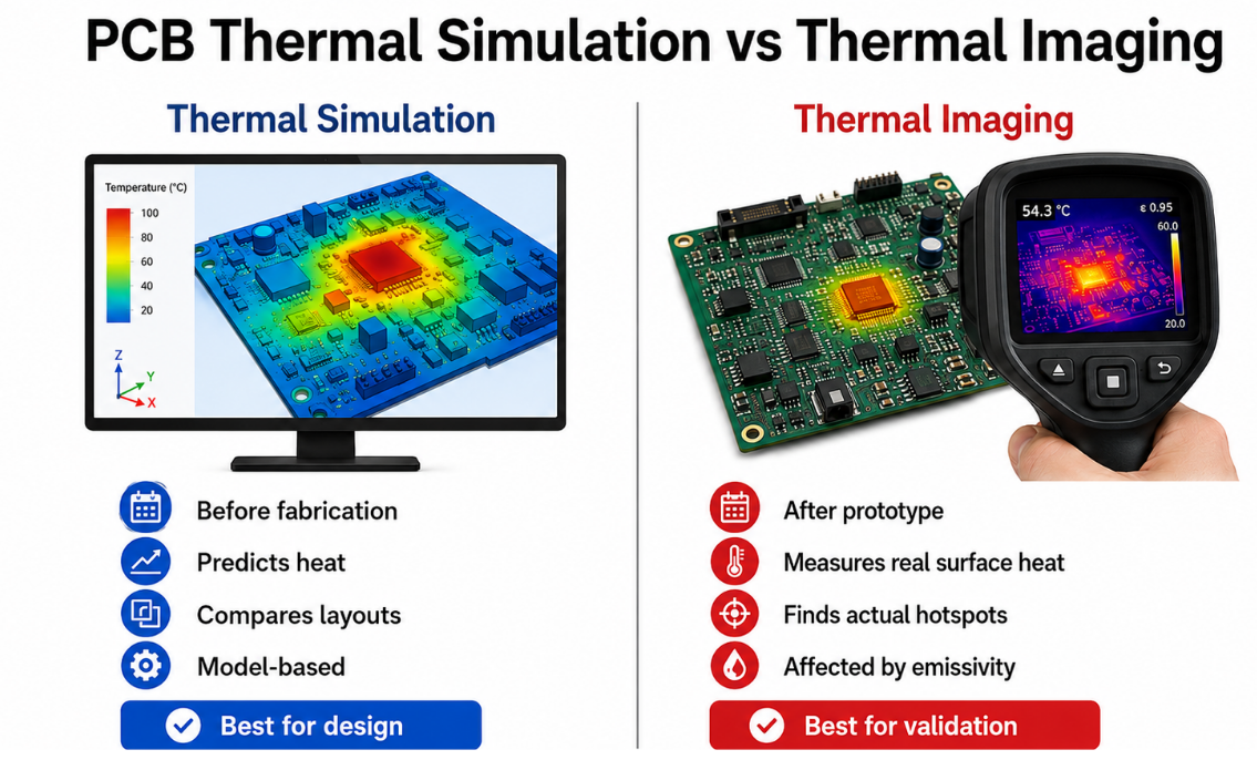
A PCB thermal hotspot map from simulation predicts heat before the PCB is built, while thermal imaging measures heat on a real powered PCB. Simulation is better for early layout comparison, and thermal imaging is better for prototype and production validation.
| Item | Thermal Simulation | Thermal Imaging |
|---|---|---|
| Use Stage | Before fabrication | Prototype or finished PCB |
| Output | Predicted temperature map | Real surface temperature image |
| Input | Stackup, copper, power loss, airflow, material | Powered PCB, load, camera, emissivity setting |
| Strength | Compares layout choices early | Shows actual heating behavior |
| Weakness | Accuracy depends on input data | May miss heat inside inner layers |
| Best Use | Copper area, via count, airflow, material comparison | Hotspot confirmation under real load |
| Accuracy Risk | Wrong power loss or material data | Wrong emissivity, angle, reflection, focus |
| Hidden Heat | Can estimate internal heat | Mainly reads visible surface heat |
| Cost Impact | Reduces trial-and-error prototypes | Finds real issues after build |
| Best Result | Used before prototype | Used after prototype |
The best approach is to use both. Simulation helps prevent heat problems early, while thermal imaging proves whether the real PCB matches the expected thermal behavior.
What Data Should You Check Before Reading a PCB Thermal Hotspot Map?
Before reading a PCB thermal hotspot map, check the setup data first, then judge the heat pattern. A red area means little if the load, ambient temperature, airflow, and temperature scale are missing.
| Data | What to Check | Why It Matters |
|---|---|---|
| Ambient | Room or chamber temperature | Higher ambient reduces thermal margin |
| Load | Voltage, current, duty cycle | Heat changes with real power loss |
| Test Time | Time to stable temperature | Short tests may miss slow heat rise |
| Airflow | Natural, forced, blocked | Cooling changes the map result |
| Enclosure | Open PCB or closed housing | Housing can trap heat |
| Scale | Minimum and maximum temperature | Color alone can mislead |
| Emissivity | Solder mask, metal, shiny surface | Wrong setting changes IR readings |
| Stackup | Layers, dielectric, copper weight | Controls heat spreading |
| Copper | Trace width, copper area, planes | Affects resistance and heat path |
| Vias | Count, size, plating, position | Affects vertical heat transfer |
| Components | Rating, power loss, spacing | Defines thermal limit |
| Material | FR-4, metal core, copper base, ceramic | Changes heat conduction |
| Limit | Case, junction, solder, PCB margin | Defines pass or fail result |
| Repeatability | Same setup across samples | Confirms stable production behavior |
A PCB thermal hotspot map should always be read with its test condition. The same color can mean safe operation in one setup and serious risk in another.
What Do Different Colors Mean on a PCB Thermal Hotspot Map?
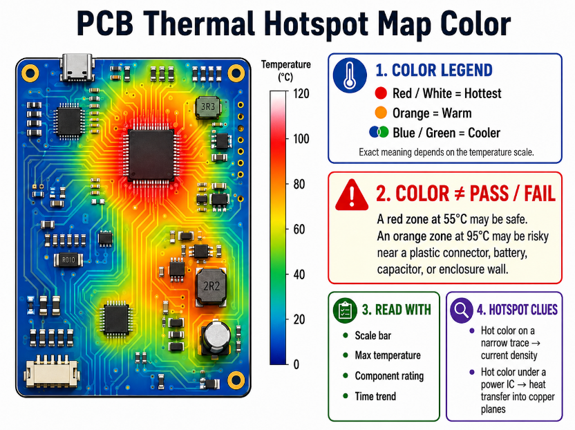
Colors on a PCB thermal hotspot map show relative heat zones. Red or white usually marks the hottest area, orange shows warm areas, and blue or green shows cooler areas. The exact meaning depends on the temperature scale.
Do not treat color as a pass or fail result. A red zone at 55°C may be safe for one product, while an orange zone at 95°C may be risky near a plastic connector, battery, capacitor, or enclosure wall.
Read the PCB thermal hotspot map with the scale bar, maximum temperature, nearby component rating, and time trend. If the hot color follows a narrow trace, the issue may be current density. If it stays under a power IC, the issue may be heat transfer into copper planes.
How Do You Read a PCB Thermal Hotspot Map Correctly?
To read a PCB thermal hotspot map correctly, start from the temperature value, then connect the heat pattern with the PCB structure. The hottest color is only the first clue.
Step 1: Read the temperature scale.
Check the maximum and minimum temperature on the map. Do not judge the result by red, orange, or blue alone because every map may use a different color range.
Step 2: Locate the highest-temperature area.
Find the hottest component, trace, pad, connector, or copper region. Then check whether the heat is concentrated in a small point or spread across a larger area.
Step 3: Compare with component limits.
Check the part rating, case temperature, junction temperature, derating rule, and nearby heat-sensitive components. A hotspot is serious when thermal margin is too small.
Step 4: Trace the heat path.
Follow how heat moves from the source into copper, vias, planes, enclosure, or airflow. If heat stays in one narrow zone, the layout may have weak copper spreading or poor via transfer.
Step 5: Compare load and time behavior.
Check whether the hotspot rises quickly, grows slowly, or stabilizes. A slow increase may point to enclosure heat buildup or insufficient thermal mass.
Step 6: Confirm uncertain readings.
Use a thermocouple or sensor to confirm suspicious points, especially on shiny copper, metal surfaces, or small packages. Good reading means matching the map with measurable temperature evidence.
What Temperature Is Considered High on a PCB Heat Map?
A high temperature on a PCB heat map depends on component rating, ambient temperature, material limit, solder reliability, and thermal margin. There is no single safe number for every PCB.
In many commercial products, a PCB surface area above 85°C deserves review, especially near plastic parts, electrolytic capacitors, batteries, displays, or hand-contact areas. For industrial, automotive, or power electronics, the allowed value depends on product class, duty cycle, enclosure, and component derating.
Use this judgment method when the PCB thermal hotspot map shows a high value:
- Compare the hotspot with component case or junction limits.
- Check long-term operating temperature, not only peak temperature.
- Review material Tg and solder joint fatigue risk.
- Leave margin for high ambient conditions.
Temperature must be judged by margin, not by color alone.
What Causes Thermal Hotspots on a PCB?
PCB thermal hotspots usually come from high power loss, high current density, weak copper spreading, poor via transfer, crowded placement, or blocked cooling. A PCB thermal hotspot map helps show which factor is most likely causing the problem.
- High-current traces
Narrow traces create higher resistance and temperature rise. The map may show a thin hot line along the current path, especially near connectors, MOSFETs, fuses, and power input areas. - Power components
MOSFETs, regulators, LEDs, current sense resistors, inductors, transformers, battery charging ICs, motor driver ICs, BGA processors, CPUs, FPGAs, and power modules can create local heat when the package cannot transfer heat into copper fast enough. - Small copper area
A power pad without enough copper cannot spread heat well. The hotspot may stay under the component instead of spreading outward into planes or wider copper regions. - Poor thermal vias
Too few vias, vias placed too far from the heat source, or weak via-to-plane connection can block vertical heat transfer. - Split or broken planes
Copper gaps under hot components can interrupt both current return and heat spreading. - Crowded placement
Several hot parts placed together can raise local board temperature and reduce cooling space. - Enclosure and airflow limits
A PCB may pass open-air testing but fail inside a closed housing because heat has no clear escape path.
Most PCB hotspots are caused by several small design and operating factors working together, not by one single component.
How Do Trace Width, Copper Area and Current Affect PCB Heat?
Trace width, copper area, and current affect PCB heat because current flowing through copper creates power loss, and narrow copper raises resistance. When current is high, a thin trace may become a visible hot line on a PCB thermal hotspot map.
Wider traces reduce current density and help lower temperature rise. Larger copper areas spread heat away from pads, ICs, MOSFETs, connectors, and resistors. Heavier copper can also improve current carrying ability, but it must match spacing, etching, and fabrication limits.
Copper must be connected to a real heat path. A large copper pour with poor connection to vias, planes, or cooling surfaces may have limited effect. For high-current PCB sections, the copper path should be short, wide, continuous, and supported by enough planes or thermal vias.
Useful design checks include:
- Avoid narrow neck-down sections in power routes.
- Increase trace width near high-current connectors.
- Use copper pours around heat sources.
- Connect copper to inner or bottom planes.
- Keep return paths short and direct.
- Use heavier copper only when the process can support it.
Good copper design reduces both electrical resistance and local heat concentration.
How Do Vias and PCB Layers Affect Heat Spreading?
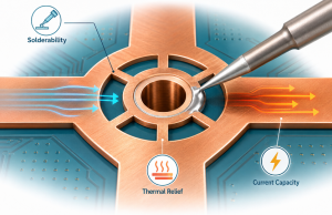
Vias and PCB layers affect heat spreading because heat can move from a hot top-layer component into inner planes, bottom copper, or metal housing through plated vias. This makes the heat path wider and lowers local temperature.
Thermal vias work best when they are placed directly under or near exposed pads. A via array can move heat downward better than one or two isolated vias. However, the vias must connect to enough copper area. If the bottom layer or inner plane is too small, the heat transfer benefit becomes limited.
PCB layers also matter. Inner copper planes can spread heat laterally, while bottom copper can help release heat into airflow or a metal base. A four-layer or multilayer PCB may improve heat spreading only when the planes are continuous and connected to the hot area.
Important checks include:
- Place vias close to the heat source.
- Use enough via quantity for the heat load.
- Connect vias directly to copper planes.
- Use filled or capped vias when solder wicking is a risk.
- Keep inner copper continuous under hot components.
- Balance copper to reduce warpage risk.
Layer count alone does not fix heat. The heat path must be connected, wide, and practical for manufacturing.
How Can You Find PCB Thermal Hotspots During Testing?
To find PCB thermal hotspots during testing, power the PCB under realistic conditions and record temperature until the heat pattern becomes stable. Testing should show how the PCB behaves in actual use, not only during a short bench check.
- Set realistic load
Use normal load, peak load, and worst-case duty cycle. The PCB thermal hotspot map should reflect actual voltage, current, and power loss. - Control ambient temperature
Record room or chamber temperature. A board that passes at 25°C may fail at higher ambient temperature. - Test with airflow conditions
Check natural cooling, forced airflow, or blocked airflow according to the final product environment. - Include the enclosure when required
If the product works inside a housing, test it inside the housing. Enclosure heat buildup can create a stronger hotspot. - Scan the full PCB first
Use thermal imaging to find hot zones around ICs, MOSFETs, LEDs, inductors, connectors, and high-current traces. - Confirm suspicious points
Use thermocouples or sensors on critical parts, especially where shiny copper or small packages may affect camera accuracy. - Record time behavior
Track whether temperature rises quickly, slowly, or stabilizes. A delayed hotspot is often missed by short testing.
How Can You Reduce PCB Thermal Hotspots in Layout Design?
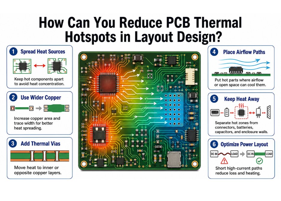
PCB thermal hotspots can be reduced by lowering heat generation, spreading heat through copper, moving heat through vias, improving airflow, and selecting a suitable material. The fix should match the cause shown on the PCB thermal hotspot map.
- Increase copper near heat sources
Add copper pours around MOSFETs, regulators, LEDs, and power resistors. Copper spreads heat and reduces local temperature. - Widen high-current traces
Wider traces lower resistance and reduce temperature rise in power paths. - Add thermal vias
Place via arrays under exposed pads and connect them to inner or bottom copper planes. - Keep planes continuous
Avoid copper splits below hot components when possible. Continuous planes spread heat more effectively. - Separate hot and sensitive parts
Keep capacitors, batteries, connectors, sensors, and plastic parts away from high-temperature zones. - Use airflow wisely
Place hot components where airflow can carry heat away instead of trapping heat behind taller parts. - Improve the heat path to housing
Use heat sinks, thermal pads, metal base contact, or copper base structures when the enclosure can help dissipate heat. - Select proper material
Use heavy copper PCB, metal core PCB, copper base PCB, or ceramic PCB when standard FR-4 cannot provide enough thermal margin.
The goal is not only a lower peak temperature. The goal is a stable, repeatable, and manufacturable thermal design.
What Common Mistakes Make PCB Hotspots Worse?
PCB hotspots often become worse when the layout blocks heat flow or when the PCB thermal hotspot map is read without checking actual conditions. The solution is to correct the cause, not only cool the visible red area.
- Mistake: Judging color without reading the scale
Solution: Always check maximum temperature, minimum temperature, ambient temperature, and color range before making a decision. - Mistake: Testing only in open air
Solution: Test inside the final enclosure when the product works in a housing. - Mistake: Using too few thermal vias
Solution: Add a proper via array close to the exposed pad and connect it to enough copper area. - Mistake: Making power traces too narrow
Solution: Widen high-current traces and remove unnecessary neck-down sections. - Mistake: Cutting copper planes under hot parts
Solution: Keep copper planes continuous where heat spreading and current return are required. - Mistake: Adding random copper pours
Solution: Connect copper to a useful thermal or electrical path instead of leaving isolated copper. - Mistake: Placing heat-sensitive parts near heat sources
Solution: Move capacitors, batteries, connectors, and sensors away from hot components. - Mistake: Ignoring thermal camera error
Solution: Check emissivity, camera angle, focus, and confirm critical points with contact measurement.
A hotspot becomes easier to solve when the map is connected to layout, material, and test conditions.
How Do You Check Whether a PCB Hotspot Problem Is Fixed?
A PCB hotspot problem is fixed only when the revised PCB thermal hotspot map proves stable temperature under equal or tougher test conditions. The solution must be verified, not assumed.
- Compare old and new maps
Use the same voltage, current, load, ambient temperature, airflow, enclosure, board position, and test duration. - Check maximum temperature
The hottest point should drop or stay within the required margin. A smaller red area alone is not enough. - Review nearby components
Capacitors, connectors, batteries, plastic parts, sensors, and ICs near the hotspot must remain within safe limits. - Confirm time stability
The temperature should stabilize instead of slowly increasing during long operation. - Check whether new hotspots appear
A fix should not move heat into another weak area, trace, connector, or component group. - Validate solder and board reliability
Review solder joints, via quality, copper balance, warpage risk, and thermal cycling exposure. - Repeat across samples
Test more than one PCB when preparing for mass production. Repeatability confirms that the fix is stable in production, not only on one prototype.
If the revised design passes thermal, electrical, and functional checks under actual conditions, the hotspot issue can be considered controlled.
FAQs About PCB Thermal Hotspot Map
Q1: Can solder mask color affect a thermal image?
A1: Yes. Solder mask color and surface finish can affect infrared readings because different surfaces reflect and emit heat differently. Matte solder mask usually reads more consistently than shiny copper, tin, or gold. For important points, use the correct emissivity setting and confirm the value with a thermocouple or contact sensor.
Q2: Why does shiny copper look cooler or hotter than nearby areas?
A2: Shiny copper can reflect surrounding heat and confuse an infrared camera. The camera may show a false low or false high value depending on angle, reflection, and emissivity. A contact measurement should be used when shiny copper appears near the highest-temperature zone or around high-current paths.
Q3: Should a PCB be tested horizontally or vertically?
A3: The test position should match final product use. Horizontal and vertical positions can change natural airflow, heat rising direction, and enclosure heat buildup. If the final product works vertically, a horizontal bench test may give a different temperature pattern and may hide a real hotspot.
Q4: Can a PCB hotspot cause intermittent failure instead of total failure?
A4: Yes. A hotspot can cause intermittent reset, voltage drift, sensor error, unstable communication, connector heating, or shutdown protection before permanent damage appears. These problems may only show after long operation, high ambient temperature, peak load, or enclosure testing.
Q5: Does a lower component temperature always mean the PCB design is fixed?
A5: No. The component may become cooler while nearby traces, solder joints, vias, or connectors become hotter. The full PCB thermal hotspot map should be checked after any layout change. A real fix reduces total thermal risk instead of moving heat into another weak area.
Q6: Can high temperature change PCB electrical performance?
A6: Yes. Heat can increase copper resistance, shift component values, affect sensor accuracy, reduce regulator efficiency, and change timing or signal behavior in sensitive circuits. Thermal review and electrical testing should be linked when the PCB handles power, precision signals, or long operating time.
Q7: Is one thermal image enough for production approval?
A7: No. One image only shows one moment under one setup. Production approval should include stable-load testing, repeated samples, defined ambient temperature, load record, enclosure condition, and confirmation of critical points. Repeatable results are more reliable than one clean thermal image.
Q8: Can conformal coating change the thermal result?
A8: Yes. Conformal coating can slightly change surface emissivity and heat transfer. It may also make thermal camera readings more consistent on some surfaces, but it can reduce heat release in other cases. If coating is used in the final product, thermal testing should be done after coating.
Q9: What should be included in a thermal test report?
A9: A useful report should include PCB version, test load, ambient temperature, airflow, enclosure condition, test duration, maximum temperature, hotspot location, image scale, measurement method, and pass/fail limit. Without these details, the result is hard to compare or use for production decisions.
Q10: Can a PCB pass at room temperature but fail in summer conditions?
A10: Yes. Higher ambient temperature reduces thermal margin. A board that reaches 75°C at 25°C ambient may run much hotter in a sealed product or hot outdoor environment. Thermal tests should consider the highest expected operating temperature, not only a comfortable room condition.
Q11: Does PCB thickness affect thermal performance?
A11: Yes, but thickness alone does not decide thermal performance. Copper weight, copper plane area, via structure, material type, and heat path are usually more important. A thicker PCB may add thermal mass, but it may not spread heat well if copper and vias are poorly arranged.
Q12: Can assembly quality affect PCB hotspots?
A12: Yes. Poor solder voiding, weak pad wetting, wrong component placement, missing thermal pad contact, or damaged vias can increase local temperature. For power components with exposed pads, solder quality has a direct effect on heat transfer from the package into the PCB.
Conclusion
A PCB thermal hotspot map should lead to a clear production decision, not just a visual check. The most important point is that heat must be judged through temperature value, load, airflow, enclosure, copper path, vias, material, component limits, and long-term stability. When these factors are reviewed together, PCB hotspots become easier to locate, reduce, and verify.
For projects with high current, power modules, LED loads, automotive electronics, industrial control, medical electronics, or enclosed products, thermal review should be completed before mass production. Send Gerber files, stackup, copper thickness, BOM, operating load, enclosure details, and thermal targets to EBest Circuit for PCB quotation and thermal design review. Contact us at sales@bestpcbs.com.
You may also like



Tags: PCB Thermal Hotspot Map, PCB Thermal Imaging, PCB Thermal Simulation