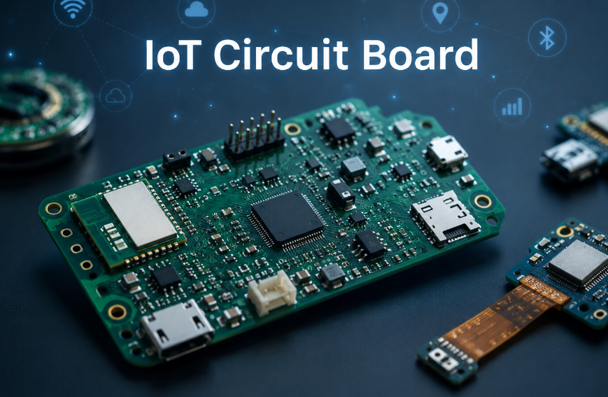
Is your IoT circuit board reliable enough for stable wireless performance, compact assembly and long-term product use? Many connected devices are small on the outside, but the internal circuit board must handle sensors, wireless modules, power control, programming interfaces and enclosure restrictions at the same time.
A well-built IoT circuit board helps improve signal stability, assembly quality and production consistency. For wearables, detectors, tracking devices and smart terminals, the right board structure, material selection, RF layout and assembly control can directly affect product reliability.
What Is an IoT Circuit Board and Why Is It Important for Smart Devices?
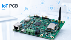
An IoT circuit board is the electronic platform that connects sensors, processors, wireless modules, power circuits and communication interfaces inside a connected device. It allows the product to collect data, process signals and send information through Wi-Fi, Bluetooth, NB-IoT, LTE-M, LoRa, Zigbee or other wireless technologies.
For smart devices, the board does much more than hold components. It affects wireless stability, battery performance, sensor accuracy, heat control, product size and assembly yield. If the PCB layout, material, soldering or testing is not controlled properly, the final device may show weak signals, unstable operation or early failure.
This is especially important for wearables and detectors because internal space is limited. A reliable IoT circuit board must support compact routing, stable grounding, clean power delivery, accurate sensor placement and proper antenna clearance.
What Types of IoT Circuit Boards Are Used in Wearables, Detectors and Smart Devices?
Different IoT products require different circuit board structures. The selection depends on product size, bending space, wireless function, assembly method and expected working environment.
| PCB Type | Common Use | Main Advantage |
|---|---|---|
| Rigid PCB | Detectors, controllers, gateways | Stable structure and mature production |
| Flexible PCB | Wearables, smart bands, compact sensors | Thin, lightweight and bendable |
| Rigid-flex PCB | Medical wearables, AI devices, compact modules | Reduces connectors and saves space |
| HDI PCB | Small IoT modules and high-density devices | Supports fine routing and compact layout |
| Metal-core PCB | Lighting IoT and heat-sensitive devices | Improves thermal control |
| Multilayer PCB | Industrial IoT and wireless terminals | Supports power, signal and ground separation |
IoT flexible circuit boards are common in wearable devices because they can fit curved spaces and moving structures. However, flexible PCB projects must confirm bend radius, copper thickness, stiffener location, connector reinforcement and coverlay opening before production.
Rigid-flex PCB is also popular in compact IoT devices. It can reduce cable connections, improve internal reliability and make assembly cleaner. For small smart products, this structure can make the whole device easier to assemble and more stable during repeated use.
Where Are IoT Circuit Boards Commonly Used?
IoT circuit boards are used in connected products that collect, process and transmit data. These products often combine sensors, wireless modules, batteries, displays, buttons, alarms or cloud communication functions.
Common applications include:
- IoT wearable circuit board for smart watches, wristbands, health monitors and portable AI devices
- IoT detector circuit board for smoke detection, gas detection, motion detection and environmental monitoring
- Smart home sensors for temperature, humidity, light, door status and water leakage
- Industrial IoT modules for equipment monitoring, remote control and predictive maintenance
- Asset tracking devices using GPS, BLE, NB-IoT, LTE-M or LoRa communication
- Smart agriculture sensors for soil, moisture, weather and irrigation control
- Healthcare monitoring devices with compact sensing and wireless transmission
- Access control terminals, wireless alarms and smart security devices
In these applications, the IoT circuit board must support stable wireless communication, accurate signal capture and reliable assembly. A small layout issue can affect connection range, sensing accuracy or long-term operation.
What Challenges Occur When Designing Printed Circuit Boards in IoT?
Designing printed circuit boards in IoT is challenging because wireless performance, sensor accuracy, power management and product size often compete for limited space. A board may pass basic testing on a workbench but perform poorly after being installed inside the final enclosure.
Common challenges include:
- Poor antenna clearance causing weak wireless range
- Noisy power circuits affecting sensors, RF modules or MCU stability
- Battery placement blocking antenna radiation or increasing local heat
- Grounding mistakes causing interference and unstable signals
- Dense routing creating crosstalk or assembly difficulty
- Connector stress in wearable and portable devices
- Insufficient test points slowing programming and inspection
- Wrong flexible area design causing copper cracks after bending
In IoT products, the PCB, antenna, battery, enclosure and firmware interface should be reviewed together. A board that works in open-air testing may behave differently inside a plastic shell, metal frame or wearable housing.
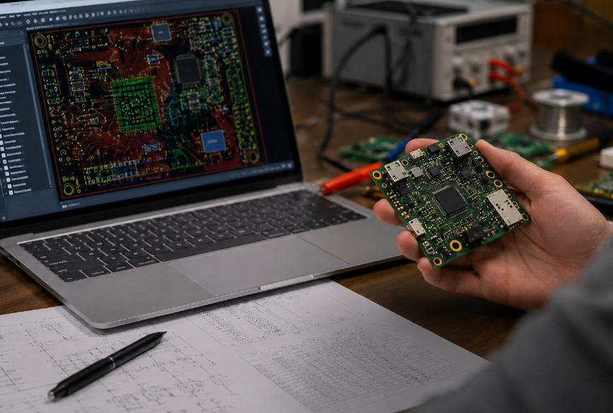
How to Design an IoT Circuit Board for Stable Wireless Performance?
A stable IoT circuit board starts with proper RF planning, clean power delivery and careful component placement. Wireless performance should be considered before routing, enclosure design and assembly confirmation.
- Plan the antenna area first
Keep the antenna away from batteries, metal parts, shields, connectors and dense copper areas. Reserve enough keep-out space around the antenna and avoid placing large components near the antenna radiation area. - Control the RF trace
Keep RF traces short, direct and smooth. Use controlled impedance when required by the wireless module, and avoid unnecessary vias, sharp corners, long stubs and sudden width changes. - Place RF matching components correctly
Place RF matching components close to the antenna feed point. Leave enough space for tuning components so wireless performance can be adjusted after sample testing. - Build a clean grounding structure
Use a continuous ground reference under sensitive signal areas. Avoid broken ground planes near RF traces and keep the antenna clearance area free from copper when required by the antenna type. - Separate power, RF and sensor areas
Place switching power circuits away from antennas and RF modules. Keep high-current traces away from wireless and sensor signals to reduce interference. - Use proper decoupling capacitors
Place decoupling capacitors close to IC power pins. This helps reduce voltage ripple and improves the stability of MCUs, sensors and wireless modules. - Review wireless module placement
Follow the module supplier’s layout recommendation. Keep module antennas near the board edge when required and avoid placing them under displays, batteries or metal covers. - Consider enclosure impact
Check whether the housing is plastic, metal or mixed material. Avoid placing antennas too close to screws, brackets, metal frames or battery packs. - Prepare for RF testing
Add test points for power, ground and communication interfaces. Test wireless range, signal strength and connection stability under real product conditions. - Validate with final assembly
Test the IoT circuit board with the real enclosure, battery, cable and installation method. Final wireless performance should not rely only on open-bench testing.
What Should Be Confirmed Before Manufacturing Printed Circuit Boards in IoT?
Before manufacturing printed circuit boards in IoT, the production files and technical requirements should be checked carefully. This reduces file misunderstanding, incorrect material selection, assembly delay and repeated revisions.
Confirm the following items before production:
- Gerber files and drill files
- BOM with exact part numbers and package information
- PCB stack-up, material and copper thickness
- Board thickness and surface finish
- Impedance control requirements
- Antenna clearance and RF routing notes
- Panelization method and breakaway structure
- Flexible PCB bend radius and stiffener position
- Test points for power, programming and function checking
- Assembly drawings and polarity markings
- Firmware flashing method if required
- Final functional test requirements before shipment
This confirmation is very important for compact smart devices. Wearables, detectors and wireless modules usually have tight internal space, so even small changes in board thickness, connector position or antenna area may affect final assembly.
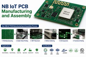
What Are the Manufacturing Processes for IoT Circuit Boards?
The manufacturing process for an IoT circuit board should control material, copper quality, hole plating, solder mask accuracy, surface finish and final inspection. Each step affects assembly accuracy and product reliability.
1. Production file review
Check Gerber files, drill files, stack-up, copper thickness and board outline. Confirm impedance control, minimum trace width, spacing, hole size, solder mask clearance, panelization and special RF notes.
2. Material preparation
Select PCB material according to board structure and application. Confirm FR4, high-Tg FR4, flexible polyimide or other required materials, as well as copper thickness and laminate thickness.
3. Inner layer imaging and etching
Transfer circuit patterns onto inner copper layers, etch unwanted copper and inspect inner circuits for opens, shorts and pattern defects.
4. Lamination
Stack inner layers, prepreg and copper foil according to the approved stack-up. Press layers under controlled temperature, pressure and time to ensure stable bonding.
5. Drilling
Drill through holes, vias, mounting holes and slots. Control hole position accuracy and clean drilled holes before plating.
6. Copper plating
Plate copper inside drilled holes to build conductive connections between layers. Control plating thickness and inspect for voids, thin copper and poor hole-wall quality.
7. Outer layer imaging and etching
Transfer outer circuit patterns, plate and etch outer copper layers. Check fine traces, pads, RF routes and connector areas.
8. Solder mask application
Apply solder mask to protect copper and prevent solder bridging. Control solder mask openings for fine-pitch pads, test points and RF areas.
9. Surface finish
Apply the required surface finish according to assembly requirements. Common options include ENIG, lead-free HASL, OSP, immersion silver and immersion tin.
10. Profiling and panel routing
Route board outlines, slots, cutouts and special shapes. Add V-cut or tab routing when required and confirm edge quality.
11. Electrical testing
Test for open circuits, short circuits and netlist consistency. Verify connectivity between layers and inspect high-risk fine-pitch or via areas.
12. Final inspection and packing
Inspect appearance, solder mask, surface finish, dimensions, warpage, scratches and exposed copper. Pack boards with moisture and handling protection.
For IoT flexible circuit boards, additional attention should be placed on polyimide material, coverlay alignment, stiffener bonding and bend-zone quality. These details help reduce cracking, delamination and connector failure during product use.
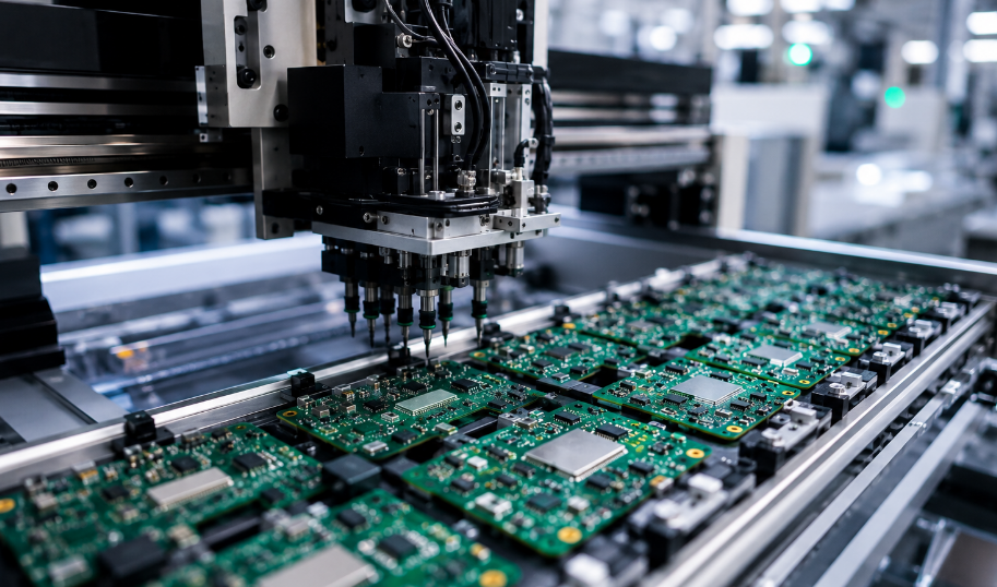
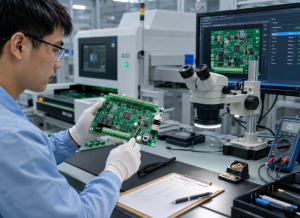
How Does IoT Circuit Board Assembly Affect Product Reliability?
IoT circuit board assembly has a direct impact on final product reliability. Many IoT devices use fine-pitch ICs, compact sensors, wireless modules, small connectors, batteries and antennas, so assembly accuracy is very important.
Important assembly controls include:
- Accurate solder paste printing for fine-pitch components
- Stable SMT placement for sensors, MCUs and wireless modules
- Controlled reflow profile to reduce solder voids and weak joints
- AOI inspection for polarity, offset, bridging and missing parts
- X-ray inspection for BGA, QFN and hidden solder joints when required
- Programming and functional testing before shipment
- Connector strength review for wearable and portable products
- Clean handling for sensors, RF areas and exposed contacts
For wearable products, the assembly process should also consider button position, battery connection, enclosure fit and charging interface alignment. For detector products, sensor direction, alarm output, wireless communication and power stability should be checked before delivery.
A reliable assembly process helps reduce field failure, restart problems, unstable signals and sensor response errors. This is why IoT circuit board manufacturing and assembly should be reviewed as one complete production flow.
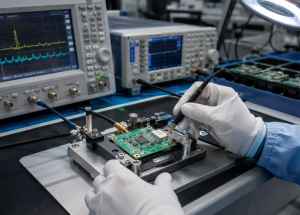
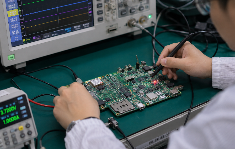
How to Test an IoT Circuit Board Before Mass Production?
An IoT circuit board should be tested for power stability, wireless performance, sensor response, assembly quality and real-use reliability before mass production. Testing should cover both the bare PCB and the assembled board.
- Check bare PCB quality
Test for opens and shorts. Check board outline, holes, slots, connector positions, solder mask quality, surface finish, scratches, exposed copper and board warpage. - Verify power circuits
Check input voltage range, output voltage, current consumption, sleep current and standby current. For battery-powered devices, check charging circuits and battery protection. - Test programming and boot function
Confirm firmware flashing, MCU boot process, reset circuit, clock signal, memory communication and programming success rate. - Test wireless communication
Check Wi-Fi, Bluetooth, NB-IoT, LTE-M, LoRa, Zigbee or other wireless functions. Measure signal strength, connection stability, reconnection ability and wireless range. - Test sensor performance
Check sensor response speed, data accuracy, calibration process and signal stability. Test sensor performance after the board is installed inside the final enclosure. - Inspect soldering quality
Use AOI to check missing parts, polarity errors, offset and solder bridging. Use X-ray for BGA, QFN, LGA and hidden solder joints when required. - Run functional testing
Check buttons, LEDs, buzzers, relays, displays, charging ports, communication ports and alarm output. Confirm all product functions against the test plan. - Run reliability checks
Perform power cycling, long-time operation, thermal behavior checks, connector plug-in tests and basic vibration, drop or bending checks when required. - Test with final assembly condition
Install the PCB inside the real enclosure. Add the final battery, cables, buttons and display, then check mechanical fit, antenna performance and heat behavior. - Approve before production
Review all test results, correct sample issues, freeze Gerber files, BOM and test procedures, then move to mass production after stable validation.
How to Choose a Reliable IoT Circuit Board Manufacturer?
Choosing a reliable IoT circuit board manufacturer should focus on production capability, assembly control, testing support and communication quality. A good manufacturer should help reduce production risk before the board enters batch production.
- Check IoT production experience
Choose a manufacturer with experience in wireless modules, sensors, batteries, compact devices, wearables and detectors. - Confirm PCB manufacturing capability
Make sure the manufacturer can support rigid PCB, flexible PCB, rigid-flex PCB, HDI PCB and multilayer PCB when required. - Review assembly capability
Check whether they can handle SMT assembly, fine-pitch ICs, QFN, BGA, sensors, connectors, shields and wireless modules. - Ask about RF and antenna awareness
A reliable supplier should understand antenna clearance, RF trace control, grounding and enclosure impact on wireless performance. - Check material and surface finish options
Confirm support for FR4, high-Tg FR4, polyimide, ENIG, lead-free HASL, OSP and other suitable options. - Confirm inspection methods
Look for electrical testing, AOI inspection, X-ray inspection, visual inspection and dimensional checking. - Check functional testing support
For IoT products, the manufacturer should support power testing, programming, wireless testing, sensor testing and final function checking. - Review file checking ability
The manufacturer should check Gerber files, BOM, stack-up, polarity markings, test points and panelization before production. - Confirm batch consistency
Ask how they control repeat orders, material traceability, soldering quality and production records. - Evaluate communication quality
Choose a manufacturer that gives clear feedback, confirms production details and points out risks before manufacturing. - Check customization support
A strong manufacturer should support custom board size, stack-up, material, assembly process and testing requirements. - Choose one-stop support when possible
For IoT circuit board projects, PCB fabrication, component sourcing, SMT assembly and testing under one supplier can reduce coordination risk.
Why Choose EBest as Your IoT Circuit Board Manufacturer?
As an IoT circuit board manufacturer, EBest provides custom IoT PCB manufacturing and assembly support for wearables, detectors, smart sensors and wireless devices. We help turn your PCB files into reliable finished boards through manufacturing review, PCB fabrication, SMT assembly and testing support.
- Custom PCB support
EBest can support rigid PCB, flexible PCB, rigid-flex PCB, HDI PCB and multilayer PCB for different IoT products. - One-stop production service
We can support PCB fabrication, component sourcing, SMT assembly, inspection and functional testing in one process. - Better risk control before production
We can review Gerber files, BOM, stack-up, assembly drawings and test requirements before manufacturing starts. - Support for compact IoT devices
We can handle fine-pitch components, sensors, connectors, batteries, wireless modules and small board layouts. - Reliable quality inspection
EBest can provide electrical testing, AOI inspection, visual inspection, dimensional checking and functional testing based on project requirements. - Support from prototype to repeat production
We can help with sample builds, production adjustment and stable batch manufacturing for long-term IoT projects.
With EBest, you get more than PCB production. You get practical manufacturing support, assembly control and quality inspection to help your IoT circuit board project move forward with less production risk.
FAQs About IoT Circuit Board
Q1: What information helps speed up an IoT circuit board project review?
A1: Complete Gerber files, BOM, PCB specifications, assembly drawings, polarity notes, test requirements and enclosure information help speed up project review. If wireless performance is important, antenna position and module details should also be included.
Q2: Can the same IoT circuit board be used for prototype and batch production?
A2: Yes, but the prototype version should be reviewed before batch production. Component availability, panelization, test points, soldering quality and enclosure fit should be confirmed before repeat orders.
Q3: What should be checked if an IoT device has unstable battery life?
A3: The main points include sleep current, standby current, regulator efficiency, wireless transmission time, sensor working cycle and charging circuit behavior. Battery life problems are often related to both circuit design and firmware settings.
Q4: How can component shortages affect an IoT circuit board order?
A4: Component shortages may delay assembly or require approved alternatives. For smoother production, the BOM should include exact part numbers, package details and acceptable substitute options when available.
Q5: What is important for wearable IoT circuit board reliability?
A5: Wearable products require attention to board thickness, flexible area bending, connector strength, battery connection, charging contacts, sweat resistance, enclosure pressure and long-term mechanical stress.
Q6: What should be checked for detector circuit boards before shipment?
A6: Detector boards should be checked for sensor response, alarm output, wireless connection, power stability, indicator status, enclosure position and final functional performance under the intended working condition.
Q7: Does an IoT circuit board always require impedance control?
A7: Not always. Impedance control is usually required when the board includes RF traces, high-speed signals or specific wireless module requirements. The final decision should follow the module datasheet and PCB stack-up plan.
Q8: What causes assembly failure in compact IoT circuit boards?
A8: Common causes include insufficient pad spacing, unclear polarity marks, missing test points, weak connector support, poor panelization, fine-pitch solder bridging and component placement too close to the enclosure wall.
Q9: How can packaging affect assembled IoT circuit boards?
A9: Poor packaging may cause moisture exposure, connector damage, board bending, surface scratches or component impact during shipping. Proper anti-static, moisture-proof and protective packing is important for assembled boards.
Q10: What should be confirmed before placing a repeat IoT circuit board order?
A10: The approved Gerber files, BOM version, firmware version, test method, surface finish, component alternatives and assembly notes should be confirmed. This helps keep repeat production consistent with the approved sample.
Request Custom IoT Circuit Board Manufacturing
EBest provides IoT circuit board products for wearables, detectors, smart sensors and connected devices. If you are preparing a new project or improving an existing board, we can support custom PCB manufacturing, assembly review, SMT assembly and functional testing.
Send your Gerber files, BOM, assembly drawings and project requirements to sales@bestpcbs.com. EBest Circuit will help review the manufacturing details, confirm the assembly approach and provide a reliable solution for your next IoT PCB order.