PCB manufacturing PCB manufacturing
Home > Blog

Exploring the Fascinating World of HDI PCBs

June 6th, 2023

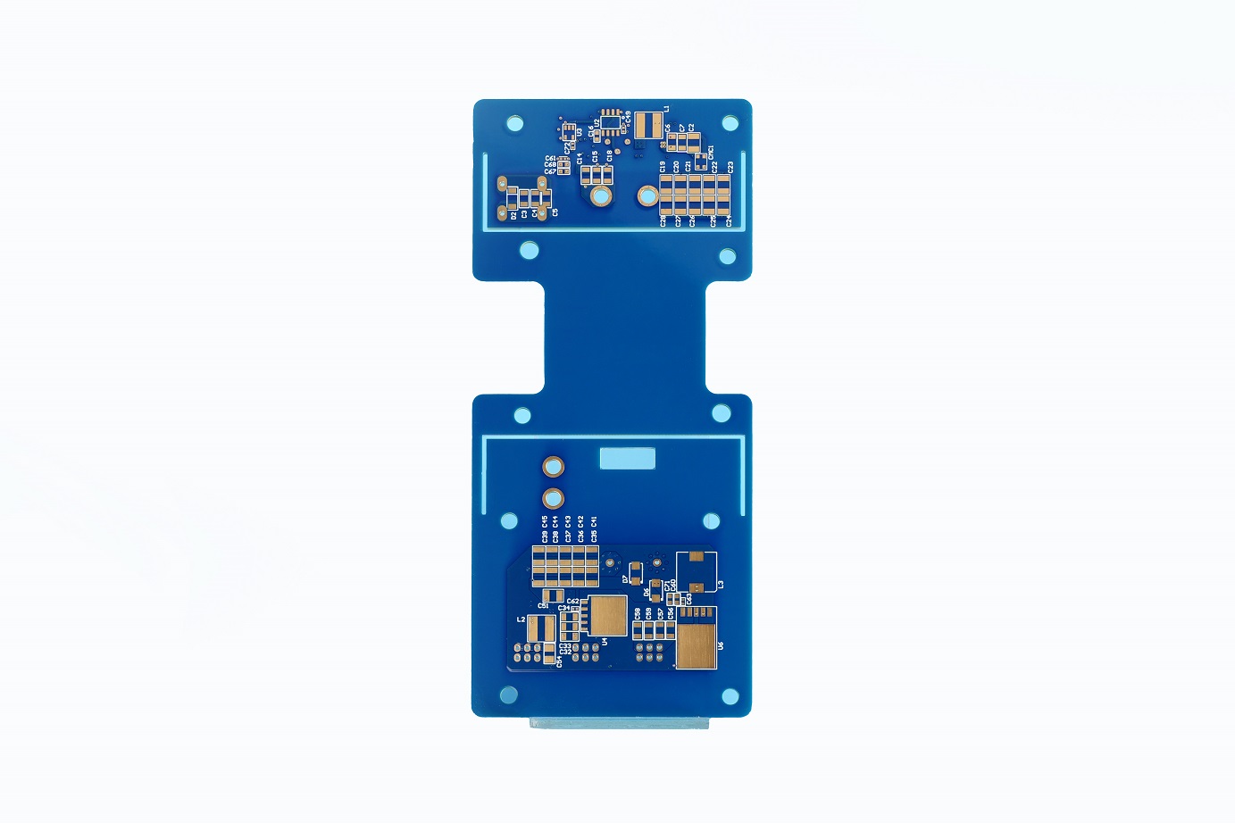
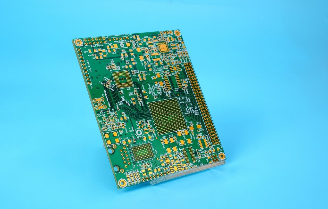
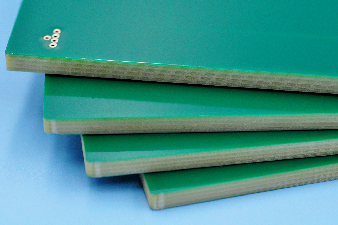
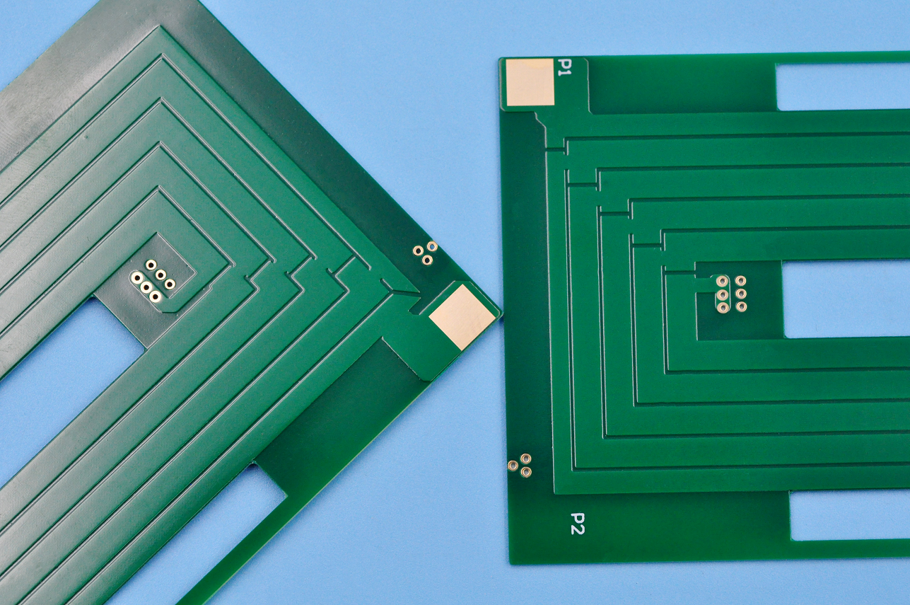
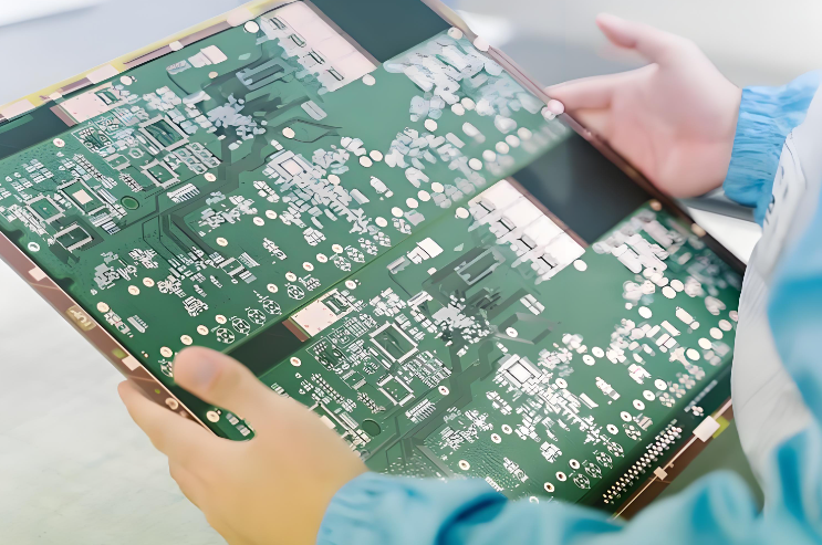
In the ever-evolving realm of printed circuit boards (PCBs), High-Density Interconnect (HDI) technology stands out as a game-changer. HDI PCBs have revolutionized the electronics industry by enabling the creation of smaller, lighter, and more advanced electronic devices. In this blog, let us delve into the captivating world of HDI PCBs, exploring their unique processes and craftsmanship. We also attached some photos for your ref.

What is HDI PCB?

HDI PCBs, short for High-Density Interconnect PCBs, are a specialized type of circuit board designed to accommodate a higher number of components within a smaller footprint. Unlike traditional FR4 PCBs, HDI boards incorporate intricate designs and advanced manufacturing techniques to achieve denser routing and interconnections.

  • Miniaturization and Component Density

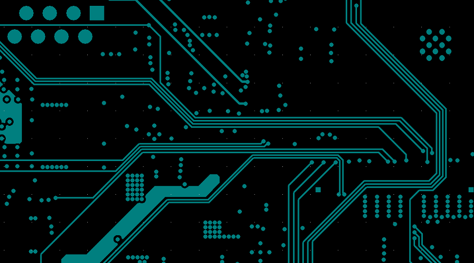
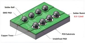
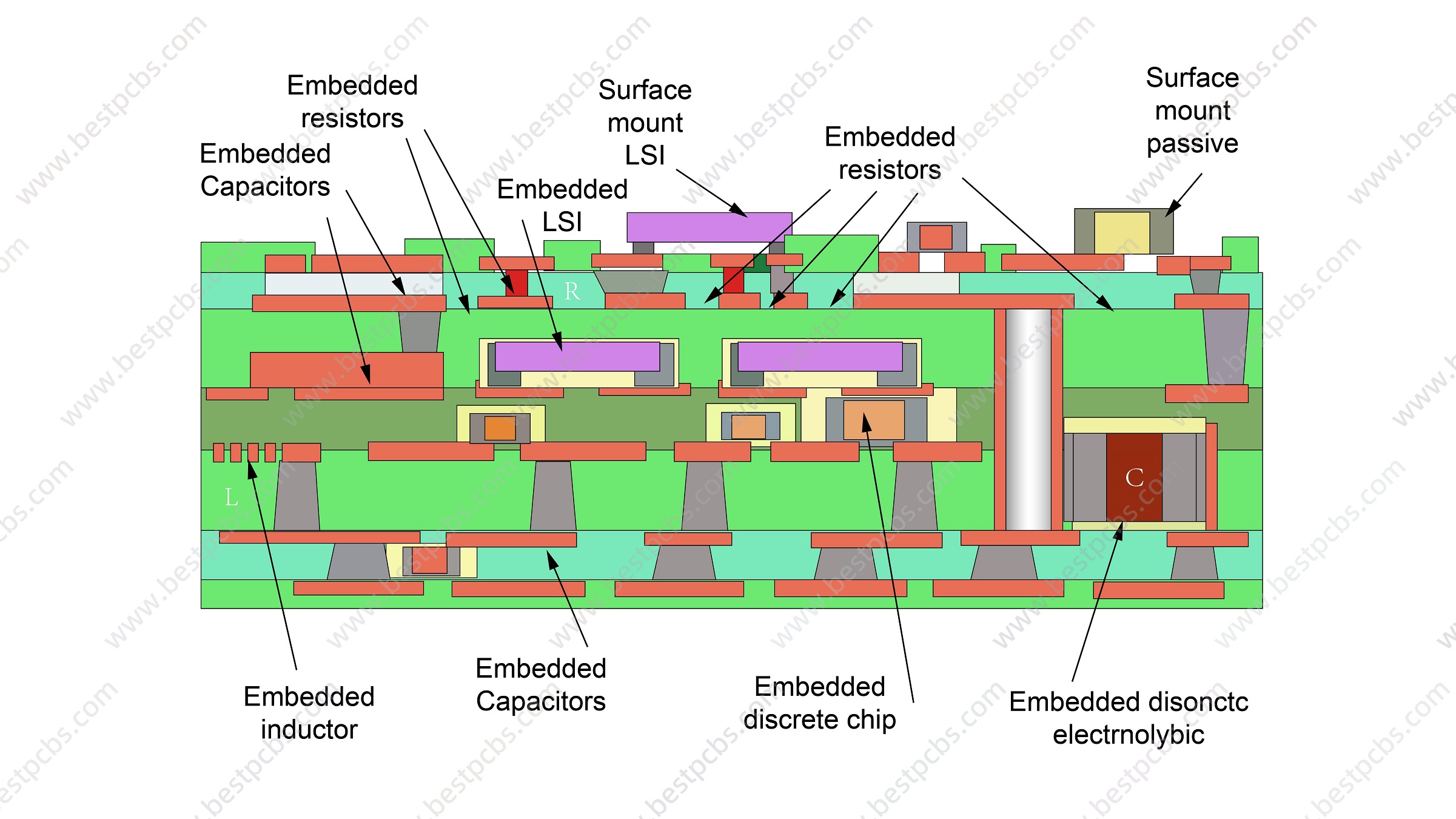
One of the standout features of HDI PCBs is their ability to achieve significant miniaturization. There are fine-pitch traces, microvias, blind and buried vias. You can see the below photo, there are many kinds of the vias.

HDI boards allow for more compact layouts and increased component density. This makes them ideal for applications where space is a premium, such as smartphones, tablets, wearables, and medical devices.

  • Advanced Manufacturing Techniques

Creating HDI PCBs involves a sophisticated blend of state-of-the-art manufacturing processes. These techniques include laser drilling, sequential lamination, and advanced imaging technologies. Laser drilling enables the creation of microvias, which are tiny holes used for interconnection between different layers of the board. Sequential lamination involves bonding multiple layers together, creating a compact stack-up with enhanced electrical performance. Advanced imaging technologies ensure precise alignment and accuracy during the fabrication process.

Benefits of HDI PCBs

HDI PCBs offer a multitude of advantages that make them highly sought after in today’s electronics industry:

1. Improved Signal Integrity: With their reduced parasitic effects and shorter signal paths, HDI boards provide superior signal integrity and enhanced electrical performance.

2. Increased Reliability: HDI PCBs minimize the risk of failures due to reduced interconnection lengths, better thermal management, and enhanced impedance control.

3. Enhanced Thermal Efficiency: The compact design of HDI boards allows for better heat dissipation and thermal management, ensuring optimal performance of heat-sensitive components.

4. Design Flexibility: HDI technology opens up new design possibilities, enabling engineers to create innovative and compact product designs without compromising on functionality.

Applications of HDI PCBs

The versatility of HDI PCBs makes them indispensable in various industries, including:

  • Consumer Electronics: Smartphones, tablets, laptops, and wearable devices.
  • Automotive Electronics: Advanced driver assistance systems (ADAS), infotainment systems, and autonomous driving technology.
  • Medical Devices: Miniature medical implants, diagnostic equipment, and patient monitoring systems.
  • Aerospace and Defense: Avionics, satellites, and military-grade electronics.
  • Industrial Automation: Robotics, control systems, and IoT devices.

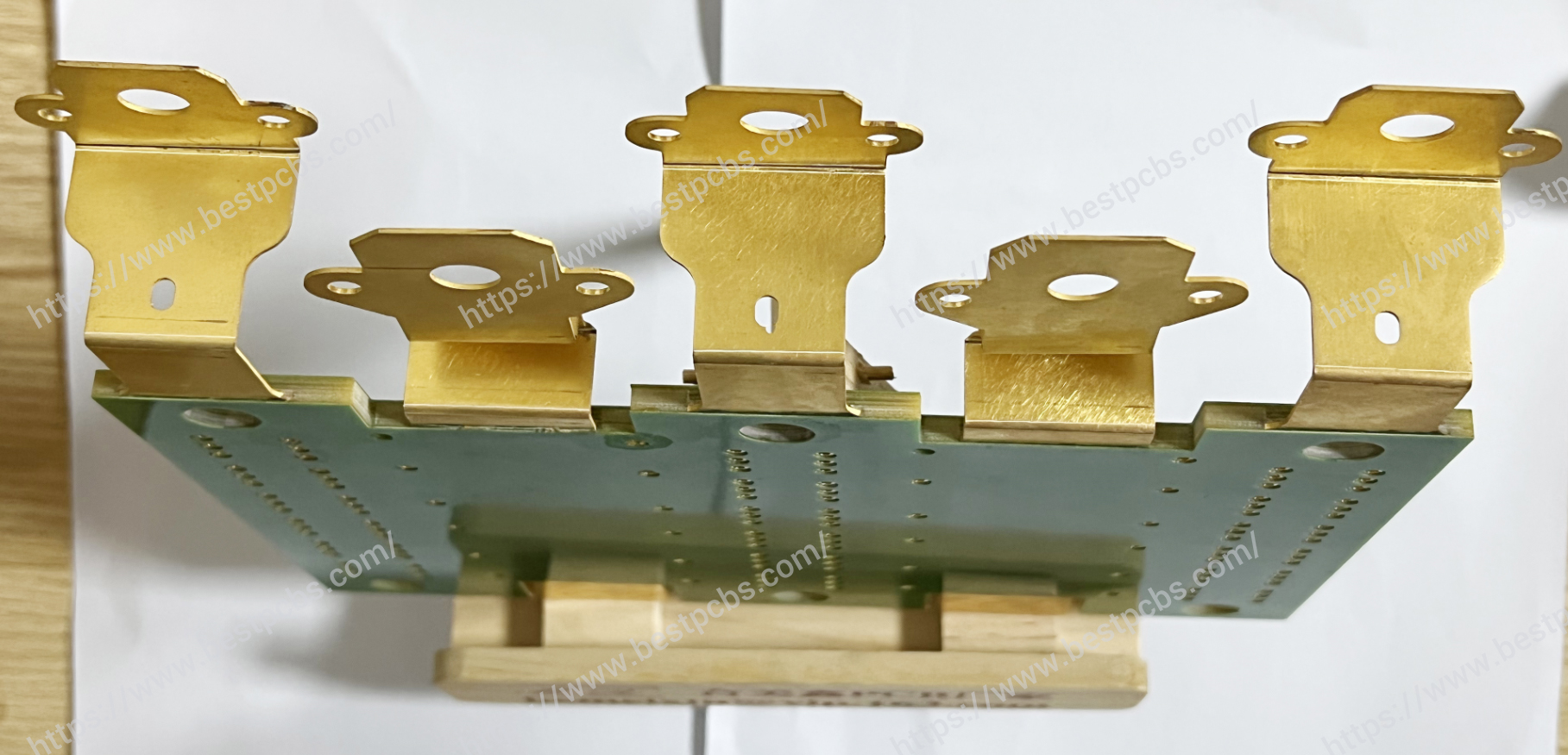
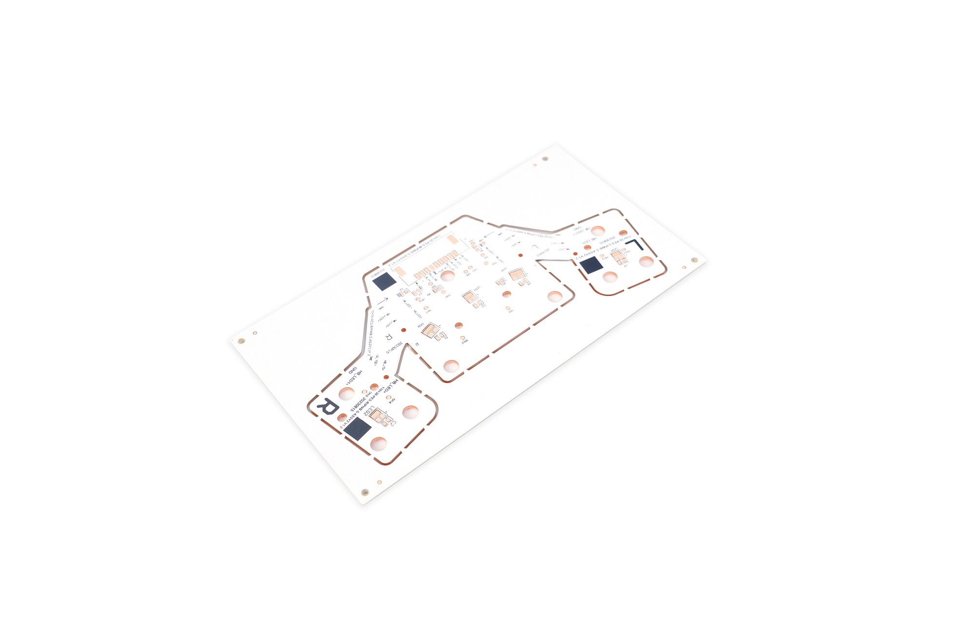
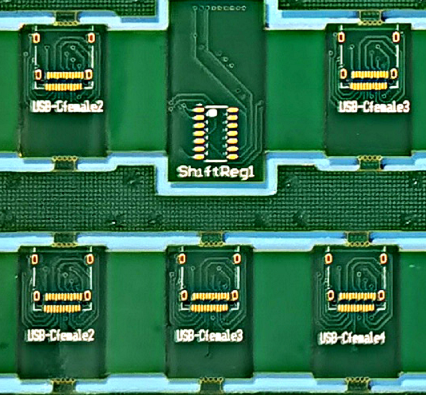
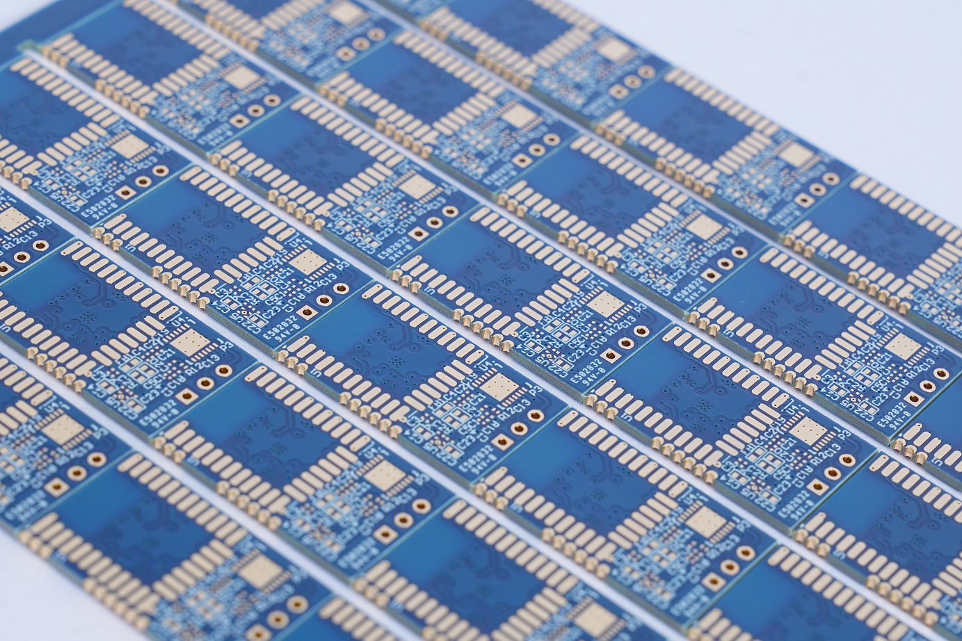
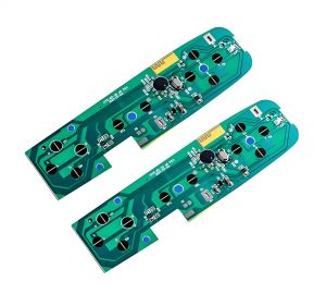
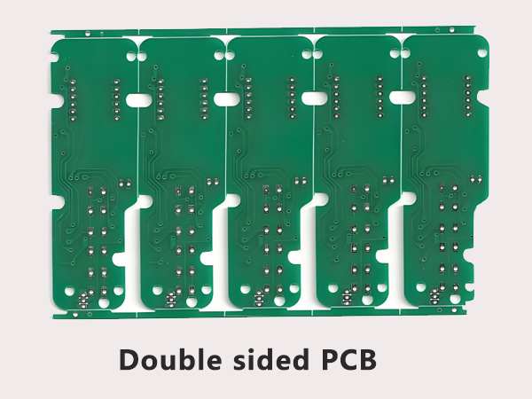
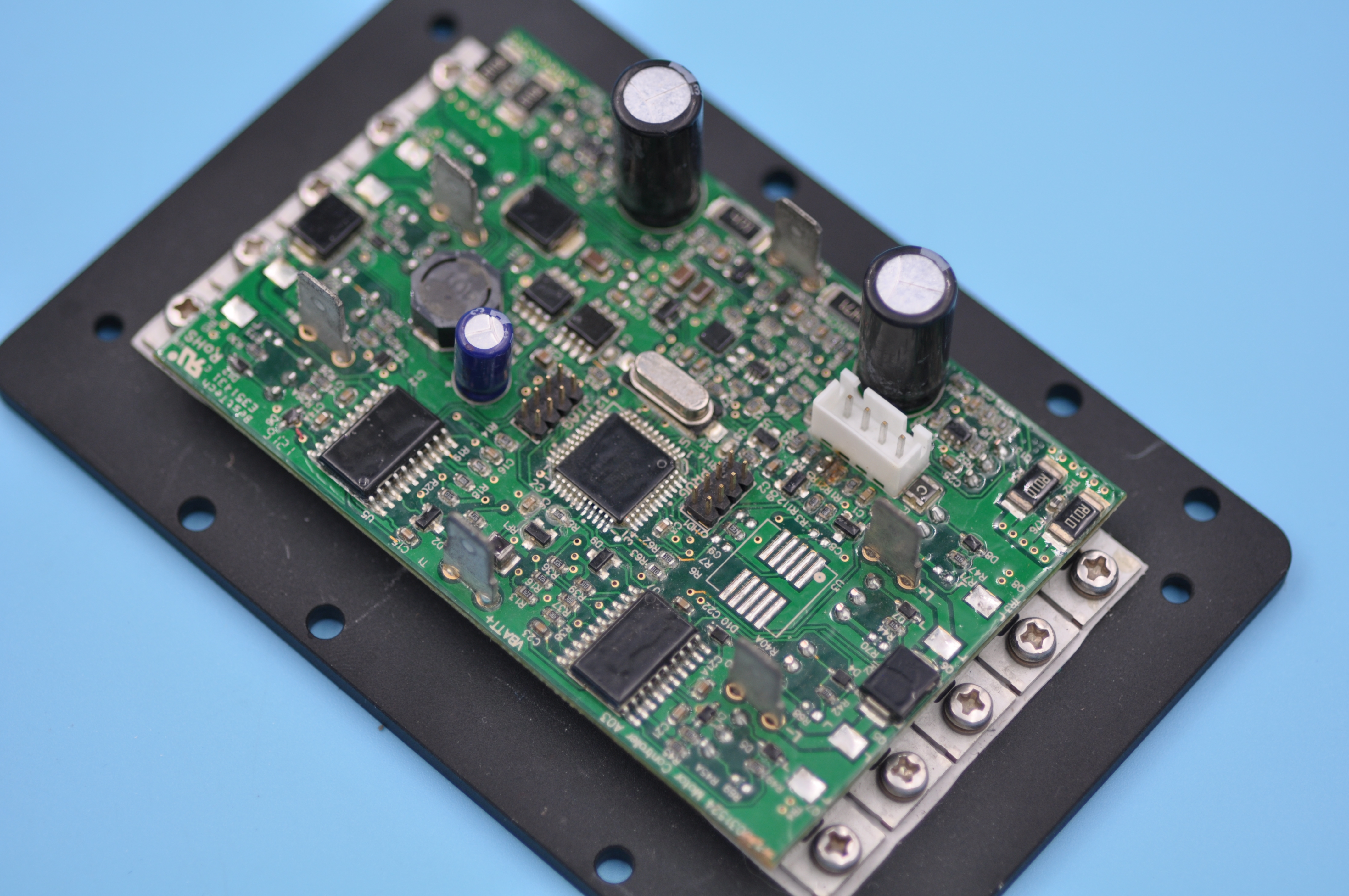
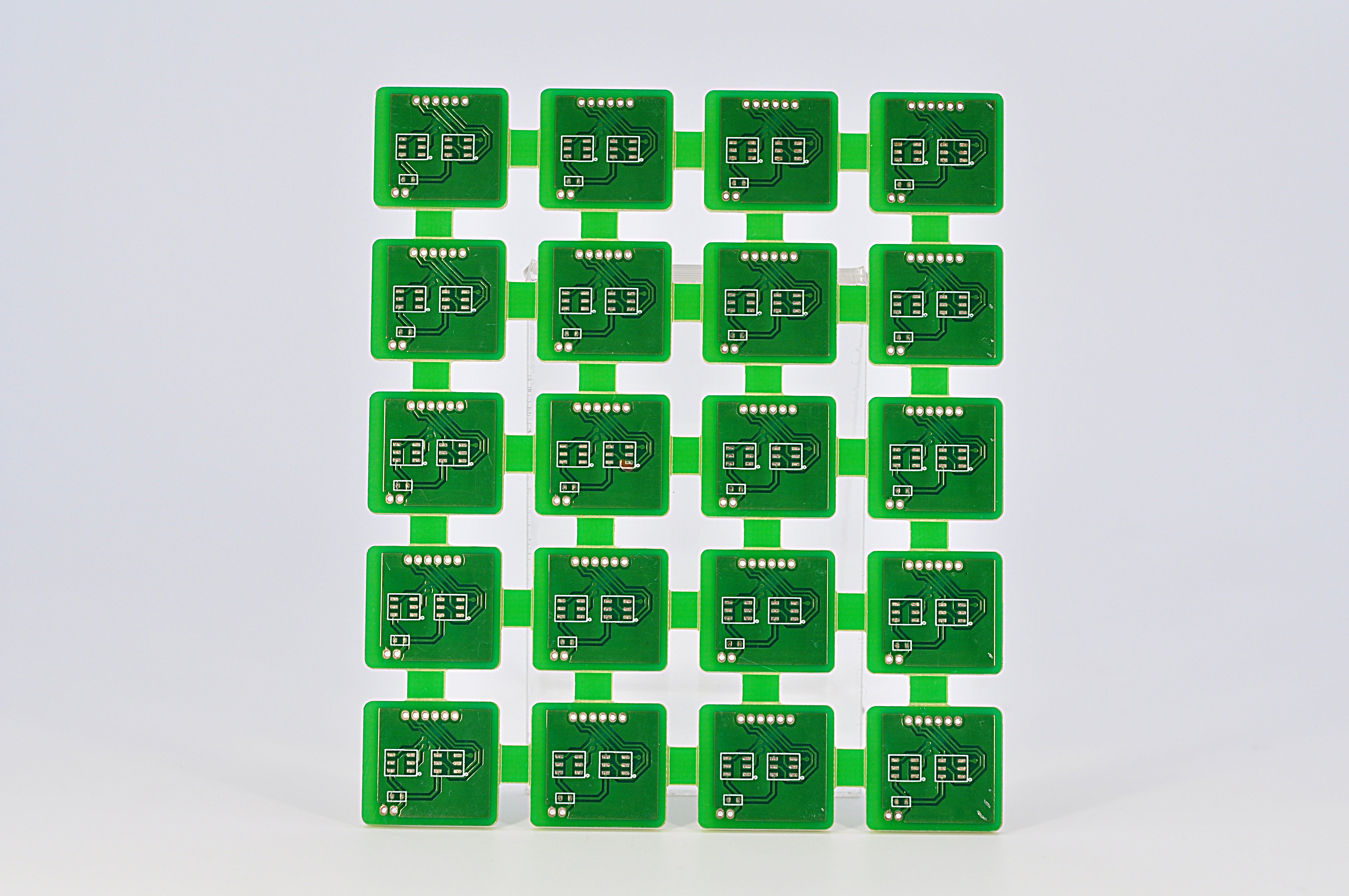
We have many customers from various industries, the PCBs of the below photos are what we produced for our customers.

Conclusion

As technology advances, HDI PCBs will undoubtedly play a crucial role in driving innovation and pushing the boundaries of what is possible in the world of electronics.

We hope this exploration into the captivating world of HDI PCBs can make you know more about HDI PCB. If you’re interested in any HDI PCB, please feel free to contact us any time. Let us supply you an excellent solution and awesome boards for you.


You may also like

5 Tips Tell You How to Solder BGA Better in PCBA

May 29th, 2023

BGA (Ball Grid Array) soldering is a widely used method in the electronics manufacturing industry for mounting integrated circuits onto printed circuit boards (PCBs). This method provides a more compact and reliable connection compared to traditional through-hole or surface mount technology (SMT). However, the complexity of BGA soldering poses various obstacles during the manufacturing process. Herein, we will explore the challenges faced in BGA soldering and discuss effective strategies to address them.

What is BGA Soldering?

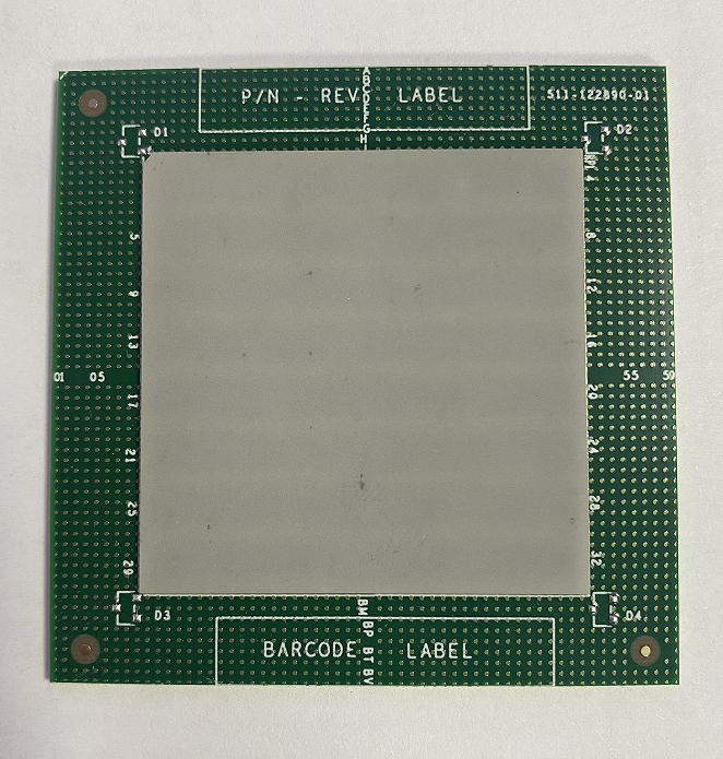
BGA soldering is a technique that involves the attachment of integrated circuit packages to a PCB using an array of solder balls. These solder balls are typically made of lead-based or lead-free alloys, depending on environmental regulations and specific requirements. The BGA package consists of a substrate, which acts as a carrier for the integrated circuit, and the solder balls that form the electrical and mechanical connections between the package and the PCB.

(BGA_balls)

The Importance of BGA Soldering in Electronics Manufacturing

BGA soldering plays a critical role in the manufacturing of various electronic devices such as computers, smartphones, and gaming consoles. The increased demand for smaller and more powerful electronics has driven the adoption of BGA packages. Their compact size and high pin density make them suitable for advanced applications where space is limited.

Challenges Faced in BGA Soldering

  • Component Alignment and Placement

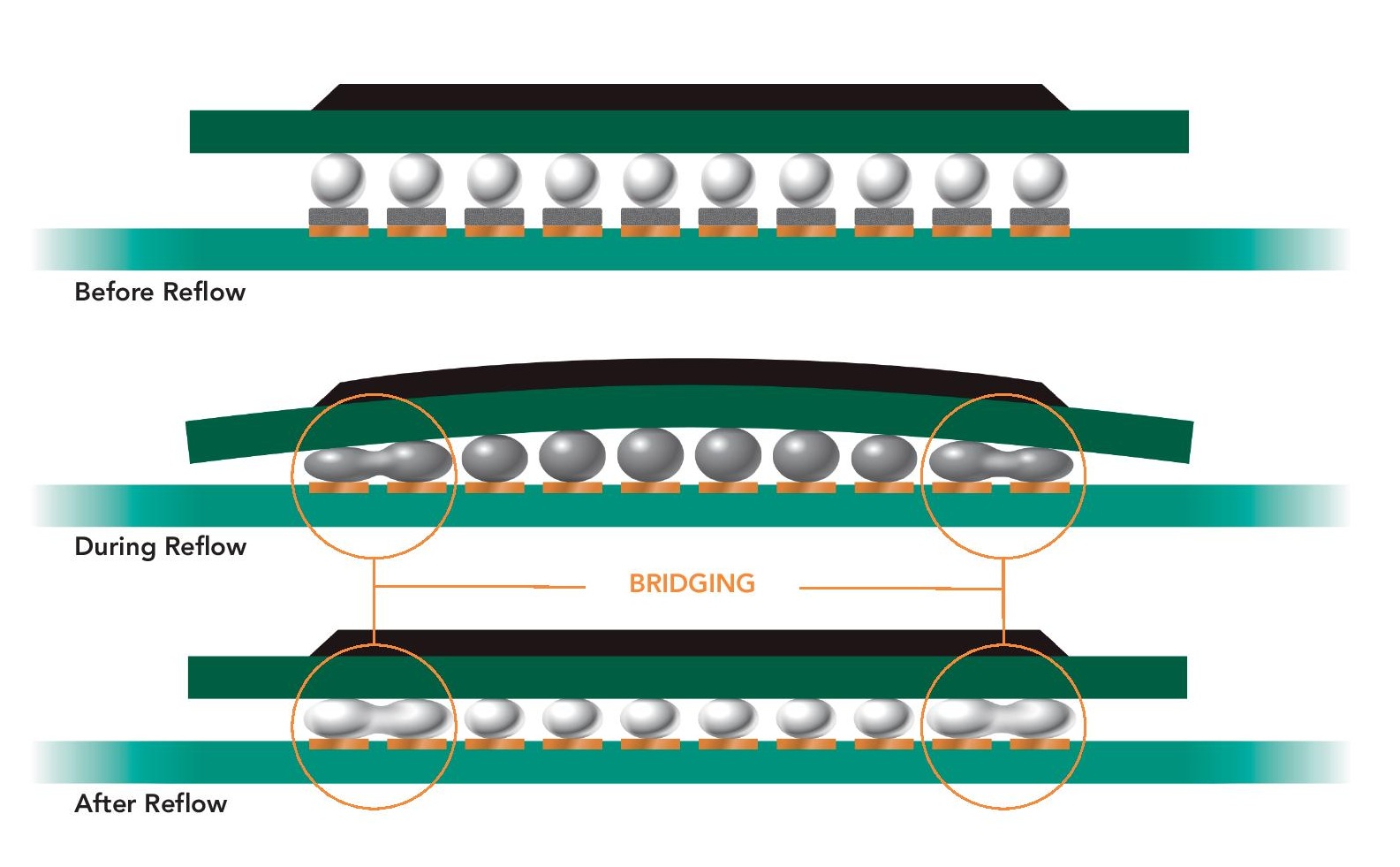
One of the primary challenges in BGA soldering is ensuring accurate component alignment and placement on the PCB. The small size of the solder balls and the dense layout of the BGA package make it difficult to achieve precise positioning. Misalignment during the assembly process can result in solder bridges, open connections, or mechanical stress on the package.

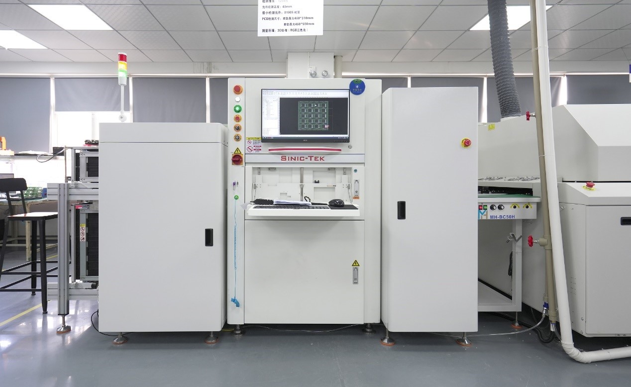
To address this challenge, manufacturers employ advanced technologies such as Automated Optical Inspection (AOI) and X-ray Inspection. AOI systems use cameras and image processing algorithms to verify the correct alignment and placement of BGA components. X-ray inspection, on the other hand, allows manufacturers to see beneath the surface of the PCB and detect any misalignment or defects that may not be visible to the naked eye.

(Alignment)
  • Solder Paste Application

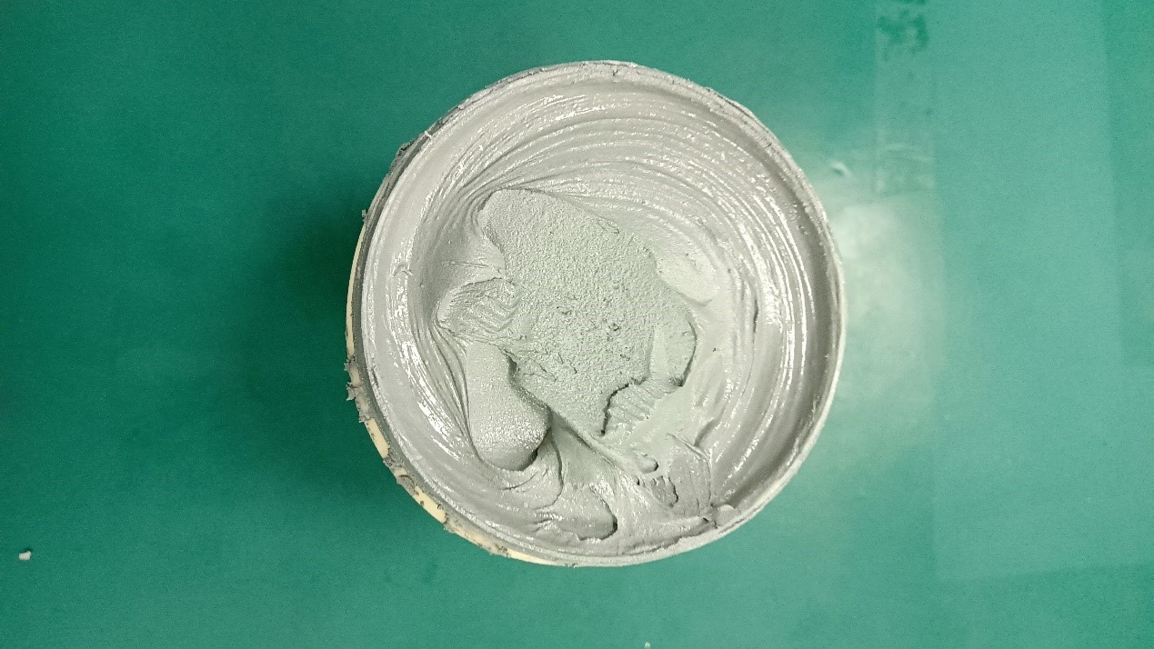
Another significant challenge in BGA soldering is achieving precise and consistent solder paste application. Solder paste, a mixture of solder alloy and flux, is applied to the PCB pads before placing the BGA package. Inadequate or excessive solder paste can lead to solder defects such as insufficient solder joints, solder voids, or solder bridging.

To overcome this challenge, careful attention must be given to stencil design and aperture selection. Stencils with appropriate thickness and properly sized apertures ensure accurate solder paste deposition. Additionally, manufacturers can employ Solder Paste Inspection (SPI) systems to verify the quality and consistency of the solder paste applied. The solder paste that EBest Circuit (Best Technology) uses is SAC305 solder paste, which has good printability and excellent stability.

(SAC305_Solder_paste)
  • Temperature Profiling

Temperature profiling, or we can say the thermal management, it is crucial in BGA soldering to ensure proper reflow of the solder paste. The reflow process involves subjecting the PCB to a carefully controlled temperature profile, allowing the solder paste to melt, form a reliable joint, and solidify. Inadequate temperature profiling can lead to insufficient solder wetting, incomplete reflow, or thermal damage to components.

Manufacturers must optimize the reflow oven setup and calibration to achieve the correct temperature profile. Thermal profiling techniques, such as the use of thermocouples and data loggers, help monitor and control the temperature during the reflow process.

  • Reflow Process

The reflow process itself presents challenges in BGA soldering. The soak zone, ramp rates, and peak temperature must be carefully controlled to prevent thermal stress on the components and ensure proper solder reflow. Inadequate temperature control or improper ramp rates can result in solder defects such as tombstoning, component warpage, or voids in the solder joints.

Manufacturers need to consider the specific requirements of the BGA package and follow recommended reflow profiles provided by component suppliers. Proper cooling after reflow is also essential to prevent thermal shock and ensure the stability of the solder joints.

(BGA_reflow)
  • Inspection and Quality Control

Inspection and quality control are critical aspects of BGA soldering to ensure the reliability and performance of the solder joints. Automated Optical Inspection (AOI) systems and X-ray inspection are commonly used to detect defects such as misalignment, insufficient solder wetting, solder bridging, or voids in the solder joints.

(AOI)

In addition to visual inspection techniques, some manufacturers may perform cross-section analysis, where a sample solder joint is cut and examined under a microscope. This analysis provides valuable information about the quality of the solder joint, such as solder wetting, void formation, or the presence of intermetallic compounds.

In a word, BGA soldering presents unique challenges in electronics manufacturing, primarily related to various factors. By addressing these challenges effectively, manufacturers can ensure the reliability and performance of BGA solder joints, contributing to the production of high-quality electronic devices. EBest Circuit (Best Technology) has rich experience in PCBA assembly and we mounted thousands PCBs for our customers, whatever it is simple design or complex design, all the products are assemble perfect and work well in customer side. Please feel free to contact us for any questions about PCBA.

You may also like

Key Challenges in Solder Mask Printing for Heavy Copper PCBs

May 23rd, 2023

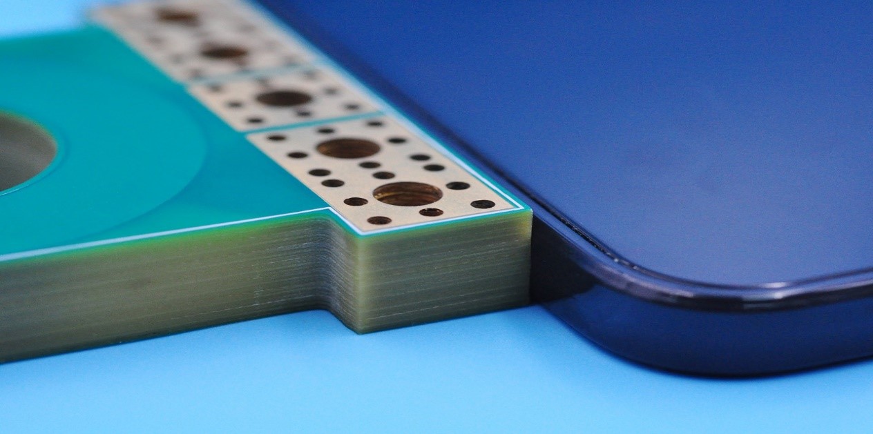
As the demand for higher power and miniaturization of electronics increases, so does the need for Heavy Copper Printed Circuit Boards (PCBs). From our last blog – Why choose Heavy Copper PCB for your High Current Project, we know the heavy copper PCBs are defined as those with copper thicknesses greater than 3 oz. These PCBs are designed to withstand high current and thermal loads, making them suitable for power electronics applications. However, the increased copper thickness also poses challenges during the solder mask printing process.

(16_layers_heavy_copper_PCB_with_10oz_each_layer)

Understanding solder mask

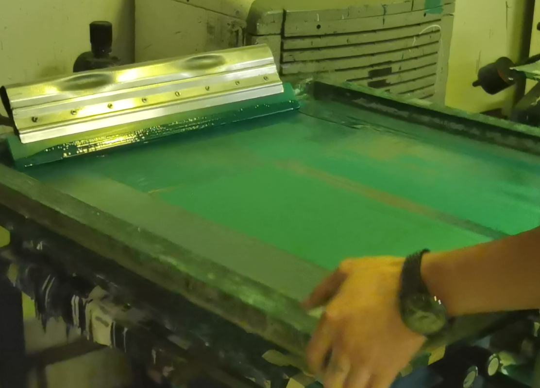
Solder mask (short for S/M in the industry) is a protective coating applied to PCBs to prevent solder bridges and improve solder joint quality. The solder mask is coated to the PCB surface using a screen-printing process, where the desired pattern is created using a stencil and the solder mask ink is then deposited onto the PCB. The ink is then cured, either through heat baking or UV light, to form a solid coating.

There are several types of solder mask materials available, including epoxy, acrylic, and liquid photo imageable (LPI) solder mask. Each type has its advantages and disadvantages, depending on the application requirements.

The benefits of using solder mask in PCB manufacturing include increased reliability, improved solderability, and reduced risk of short circuits and corrosion. The solder mask we usually use is Taiyo, which has high reliability and excellent heat resistance.

(Solder_mask_manually_printing)

Challenges in solder mask printing of heavy copper PCBs

While solder mask printing is a critical step in PCB manufacturing, the increased copper thickness in heavy copper PCBs presents several challenges for printing process as I mentioned before. It’s difficult to apply enough solder mask to cover thick copper pattern and base material with severe height difference.

1. The high copper thickness and thermal conductivity of heavy copper PCBs make it difficult for the solder mask ink to adhere properly to the surface. This can result in insufficient coverage and registration accuracy, which can affect the overall quality and reliability of the PCB.

2. The high copper thickness can cause stress on the solder mask, leading to mask cracking and peeling. The navigation mark on the substrate has specific ink thickness requirements due to limitations in the ink thickness that can be applied to the substrate. If the ink thickness on the substrate is too thick, it may result in solder resist cracks in the substrate position after the printed circuit board is soldered. This can occur during reflow soldering or thermal cycling, resulting in poor solder joint quality and reduced reliability.

3. The thick solder mask is also more difficult to exposure and develop. If the exposure energy is too weak or not enough, then some undercut problem may happen.

How to overcome this challenge?

To address these challenges, it is essential to choose the right solder mask materials and optimize the application process.

  • Choosing the right solder mask materials is crucial for ensuring proper adhesion and coverage on heavy copper PCBs. LPI solder mask is often preferred for heavy copper PCBs due to its excellent adhesion and thermal stability. However, epoxy and acrylic solder mask materials can also be used with proper surface preparation.
  • Optimizing the solder mask application process can also help address the challenges of heavy copper PCBs. This can include using a thinner stencil for improved registration accuracy and applying multiple coats of solder mask for better coverage. Advanced solder mask technology, such as laser direct imaging (LDI), can also help improve registration accuracy and reduce the risk of mask cracking and peeling.
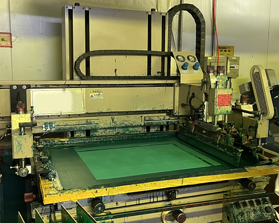
  • Optimizing the printing process, now in EBest Circuit (Best Technology), we always make the substrate first, fill the substrate with the solder mask and then treat it as a normal PCB for normal printing solder mask.
(Solder_mask_printing)

If you are in the process of designing a complex multi-layer heavy copper PCB and are looking for a high-quality and experienced manufacturer, feel free to reach out to us at sales@bestpcbs.com, EBest Circuit (Best Technology) can support you by OEM and ODM service to ensure your design is cost-effective and can be easily manufactured.

You may also like

Why choose Heavy Copper PCB for your High Current Project?

May 16th, 2023

In the world of electronics, printed circuit boards (PCBs) play a vital role in connecting and powering various components. They are the backbone of every electronic device, from smartphones to industrial machinery. When it comes to designing a PCB for a project, the thickness of the copper layer is an important consideration. Heavy Copper PCB, also known as Thick Copper PCB, has become increasingly popular in charging automotives due to their unique features and benefits. In this article, we will discuss why consider heavy copper PCBs for your high current project.

What a Heavy Copper PCB is?

A heavy copper PCB is a circuit board with an unusually thick copper layer, usually exceeding 3 ounces per square foot (oz/ftÂČ). By comparison, standard PCBs typically have a copper layer thickness of 1 oz/ftÂČ. Heavy copper PCBs are used in applications where high current is needed, or the board needs to withstand mechanical and thermal stress.

(Heavy_copper_PCB)

Benefits of Heavy Copper PCBs

  • High Current Capacity

The thicker copper layer in a heavy copper PCB allows for a higher current capacity. This makes it ideal for high-power applications such as power supplies, motor controllers, and industrial equipment. Heavy copper PCBs can carry up to 20 amps or more, compared to the standard 5-10 amps of a regular PCB.

  • Thermal Management

Heavy copper PCBs are known for their excellent thermal management capabilities. The thicker copper layer allows for better heat dissipation, reducing the risk of overheating and component failure. So that they can generate a lot of heat for the end-application.

  • Durability

Heavy copper PCBs are more robust and durable than standard PCBs. The thicker copper layer provides better mechanical support, making them resistant to damage from vibration, shock, and bending. This makes them suitable for harsh environments and industrial applications.

  • Increased Flexibility

Heavy copper PCBs offer increased design flexibility compared to standard PCBs. The thicker copper layer allows for more complex and compact designs, reducing the overall size of the board. This makes them ideal for applications where space is limited, that means you can make a very heavy copper while the size is very small.

  • Better Signal Integrity

The thicker copper layer in heavy copper PCBs provides better signal integrity. This reduces the risk of signal loss and interference, resulting in more reliable and efficient circuit performance.

Copper thickness design for a Heavy Copper PCB?

Due to the thickness of copper in heavy copper PCB is thick then normal FR4 PCB, then it is easily to be warped if the copper thickness is not match each other in symmetrical layers. For example, if you are designing an 8 layers heavy copper PCB, then the copper thickness in each layer should follow L8=L1, L7=L2, L6=L3, L5=L4 standard.

Additionally, the relationship between minimum line space and minimum line width also should be considered, follow the design rule will help to smooth production and shorten the lead time. Below are the design rules between them, LS refers to line space and LW refers to line width.

(Heavy_copper_design_rule)

Drill hole rules for heavy copper board

A plated through hole (PTH) in printed circuit board is to connect top and bottom side to make them electricity. And when the PCB design has multi copper layers, the parameters of holes must be considered carefully, especially hole diameters.

In EBest Circuit (Best Technology), the minimum PTH diameter should be >=0.3mm while the copper ring annular should be 0.15mm at least. For wall copper thickness of PTH, 20um-25um as default, and maximum 2-5OZ (50-100um).

(16L_heavy_copper_PCB_with_35um_copper_in_via_holes)

Basic parameters of Heavy Copper PCB

Here are some basic parameters of heavy copper PCB, hope this can help you to understand EBest Circuit (Best Technology)’s capability better.

  • Base material: FR4
  • Copper thickness: 4 OZ~30 OZ
  • Extreme Heavy Copper: 20~200 OZ
  • Outline: Routing, punching, V-Cut
  • Solder mask: White/Black/Blue/Green/Red Oil (Solder mask printing is not easy in heavy copper PCB.)
  • Surface finishing: Immersion Gold, HASL, OSP
  • Max Panel size: 580*480mm (22.8″*18.9″)

Applications of Heavy Copper PCBs

Heavy copper PCBs are used in a variety of applications, including:

  • Power supplies
  • Motor controllers
  • Industrial machinery
  • Automotive electronics
  • Aerospace and defense systems
  • Solar inverters
  • LED lighting
(Heavy_copper_PCB_for_high_power_supply)

Choosing the right PCB thickness is crucial for the success of any project. Heavy copper PCBs offer unique features and benefits that make them ideal for high-power and high-temperature applications. If you want to ensure the reliability and performance of your project, consider using heavy copper PCBs. EBest Circuit (Best Technology) has more than 16 years manufacturing experience in heavy copper PCBs, so we are so confident that we can be your most reliable supplier in China. Welcome to contact us at any time for any questions or any queries about PCBs.

You may also like

5 PCB Testing details to make your PCB no more quality issues

April 24th, 2023

As we all know, it is very important to get a well-functional PCB from the PCB manufacturers.  A well functional PCB means that the electricity testing has been performed well at the PCB manufacturer end. However, you may have found some PCB you purchased are with some electricity issues like short & open circuits, or some visual issues like solder pad missing., etc.

Do you know how this issue come while the PCB testing process?

According to the feedback come from the customers, here we summarized some improper ways during the PCB Electricity testing process which may lead to the PCB fail to the test.

Here are some major points for your reference:

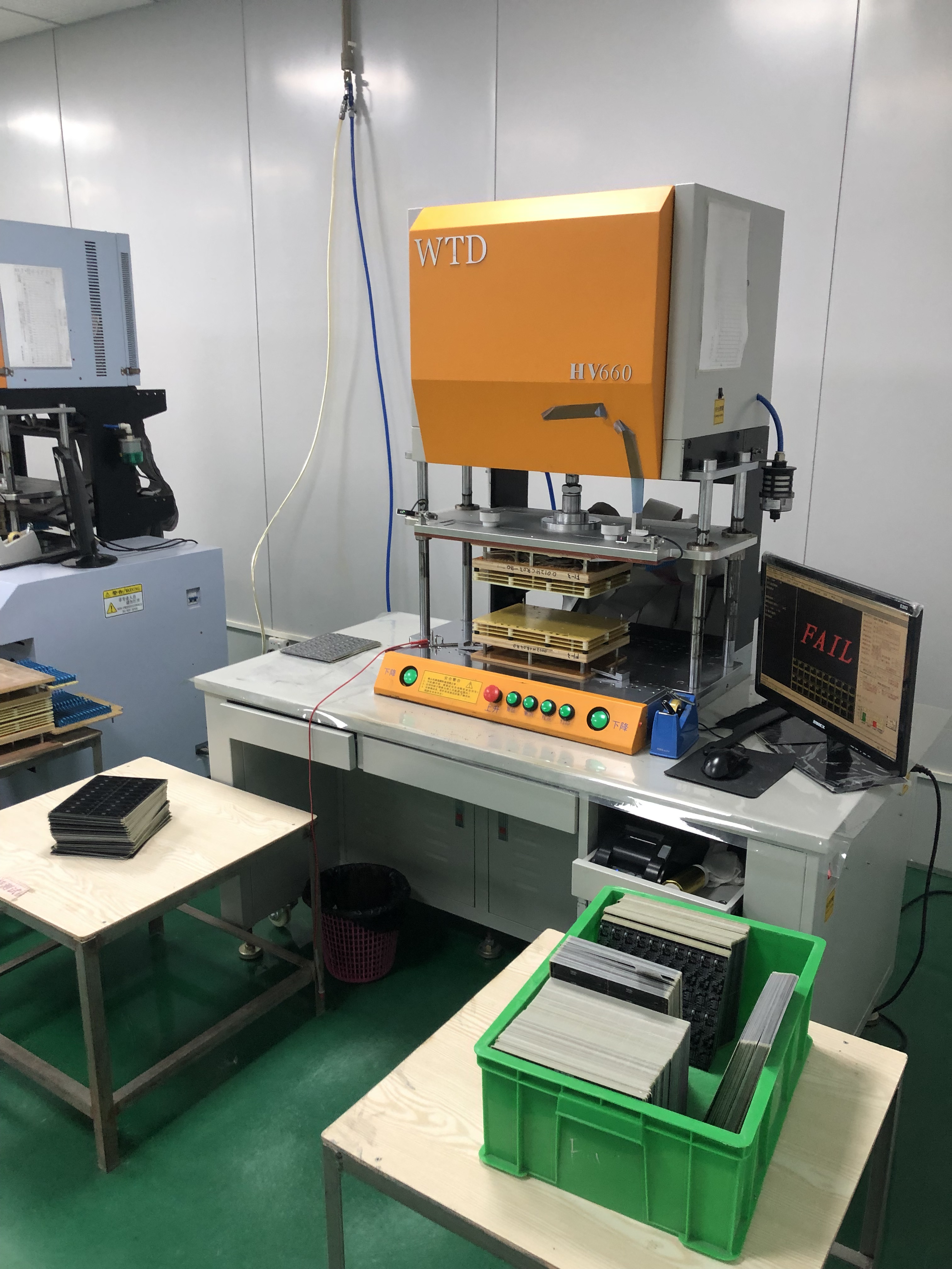
  • Incorrect direction when placing PCB board on testing worktop, the force on probes will cause indentation on boards.
  • PCB manufacturers don’t regularly maintain their testing jig, causing some malfunctions on testing jig can’t be found in time. Take the counter for example, if we do not find the counter’s fixing screw loose in time, it will cause the counter to fail to read the caliper scale. Of course, it also could be the counter is dysfunctional sometimes.
  • PCB manufacturers don’t regularly check/change the testing probes. Dirt on the testing probe cause testing results is inaccurate.
  • PCB testing operator don’t distinguish functional board from NG board due to unclear placement area.

So, if the circuit boards testing work under above improper way, do you know what effects will be on your products?

Base on some lessons learned from our customers, you may get following influences caused by improper way of the PCB testing.

Increase your quality issues

The low testing accuracy will make the functional PCB mixing together with the defective PCB.  If the PCB testing defects can’t be found in time before PCB assembly, defective products will flow into the market, which will seriously increase the quality risk hidden on the end products.

Delay your Progress

After defective PCBs are found, repairing will greatly delay the progress of the project.

Increase your overall cost

The defective PCB will cost many people and time to check and follow, this will directly to increase the overall cost of the projects.

We know deeply that poor testing will bring serious consequences for customers, so with more than 16 years experiences on Printed Circuits Board fabrication, EBest Circuit (Best Technology) has rich experiences on PCB electric testing managements, and following are some of our management solutions to control our PCB testing process:

1.   We execute strictly the pre-job training 3 months in advance for the testing operator, and all the testing will be operated by the professional and experienced testers.

2. Maintain or replace the test equipment every 3 months, and use a brush to clean the tester in a regular period or replace the pin cable head to make sure there is no contaminate at the test probe.

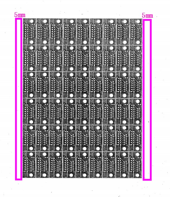
3. Add the extra tooling hole at rails for fix purpose to make sure the placement of PCB orientation is no mistake during testing process.

4. The testing workshop must be divided clearly for the qualified board and NG board, the location to keep NG board will be marked with red line.

5. The testing process must be strictly followed with our internal PCB testing standard operating procedure.

With the help from above management solutions for the PCB E-Testing during the PCB manufacturing process, the PCB we send to customers works very well, which also make sure their products can be assembled well and deliver well in the markets. For us, more and more kindly feedback regarding the functional feedback comes from our customers, here are some good feedback from customers for your reference.

If you have any questions about PCB testing or PCB manufacturing, please feel your freely to leave your message or contact us. In our next update, we will share which test methods are used in the during the PCB Assembly.

You may also like

Can I Design Via Holes in Thick Film Ceramic Boards?

April 18th, 2023

May some engineers or designers who be interested in thick film ceramic circuit are curious about can thick film ceramic boards design with via holes like FR4 PCB? Herein, we will explore the feasibility of using thick film ceramic boards for via holes, including the materials and processes involved, as well as the advantages of this approach.

What is thick film ceramic board?

The “Thick Film” refers to the thickness of conductor layer on a Ceramic PCB. Normally the thickness will be at least 10um, around 10~13um, which is thicker than spurting technology in Thin Film Ceramic PCB. And of course thickness is less than DCB Ceramic board or FR4 board.

Thick film ceramic circuit enables to put resistor, electric capacitor, conductor, semi-conductor, and interchangeable conductor on ceramic board, after manufacturing steps of printing and high temperature sintering. The more important thing is by using thick film technology, we can make all the resistors with the same value, or different value for different resistor on the same board.

Materials and processes for via holes

In general, thick film ceramic circuit is not suitable for designing via holes. Because the characteristics of thick film ceramic board mainly depends on the insulation properties of its ceramic substrate, rather than conductive properties. The conductivity of thick film ceramic plate is not good than Metal Core PCB, or even we can say it has a very poor conductivity, usually can’t meet the requirements of the via hole.

But, designing via holes in thick film ceramics is available in EBest Circuit (Best Technology). Generally speaking, the fabrication of via holes in thick film ceramic boards typically involves several key materials and processes.

From the designer’s perspective, a conductive material is used to create a continuous conductive path from one side of the ceramic board to the other. Common conductive materials include gold paste, silver paste, and copper paste. These materials are usually screen printed onto the ceramic board in the desired pattern, and then fired at high temperatures to achieve sintering and form a conductive layer.

Once the conductive layer is formed, the via holes are created by drilling or punching small holes through the ceramic board at the desired locations. These holes are then filled with a conductive material, such as silver paste or copper paste, to establish electrical connections between the different layers of the circuit.

Finally, the via holes are fired again at high temperatures to achieve sintering and ensure good adhesion and electrical performance.

Advantages of Via Holes in Thick Film Ceramic Boards

These via holes offer several advantages in the design and fabrication of thick film ceramic boards, including as following:

  • Electrical connectivity

Via holes provide electrical connectivity between different layers of a thick film ceramic board. They allow for the interconnection of different circuitry or conductive layers, enabling the flow of electrical signals or power between different parts of the board. This allows for complex and multi-layered circuit designs, which can be highly beneficial in applications that require intricate circuitry or high-density interconnects.

  • Space-saving

Via holes can provide a means of vertical interconnection, allowing for more efficient use of board real estate. Instead of routing traces or conductors on the surface of the board, which can take up valuable space, via holes can be used to route connections through the board, freeing up surface area for other components or functions. This is especially advantageous in compact or miniaturized electronic devices where space is limited.

  • Thermal management

Via holes can aid in thermal management in thick film ceramics. They can be used to transfer heat from one layer of the board to another, helping to dissipate heat generated by components or circuits. This can be particularly important in high-power or high-heat applications, where efficient thermal management is crucial for preventing overheating and ensuring reliable performance.

  • Mechanical stability

Via holes provide additional support and reinforcement to the board, reducing the risk of warping, bending, or cracking. Via holes can also help improve the overall mechanical integrity of the board by reducing stress concentration points and enhancing its structural rigidity.

  • Design flexibility

Via holes offer design flexibility in thick film ceramic boards. They can be designed and placed according to the specific requirements of the circuit or system, allowing for customized and optimized designs. Via holes can be used to route traces, create vias for component mounting, or provide grounding or shielding, among other functionalities. This flexibility in design allows for more efficient and effective circuit layouts, which can lead to improved performance and reliability.

As previously mentioned, designing via holes in thick film ceramic boards offers various benefits. However, when it comes to choosing the appropriate paste for via holes, silver paste is often recommended to our customers. But why is that? Can I use gold or copper? In our upcoming article, we will delve into the reasons behind this recommendation and provide you with valuable insights. Stay tuned to uncover the answers!

You may also like

10 Tips to Reduce the manufacturing cost of Printed Circuit Board

March 23rd, 2023

Many times, when PCB engineer or purchaser seek for a PCB manufacturer to make circuit boards, that always think the price is too high, but don’t know where makes the price is so high and how to optimize the cost on the premise of ensuring the quality of the circuit board. Herein, we share a very useful guideline about “Ten tips to reduce the PCB manufacturing cost”, welcome to read on!

  • Substrate

Different brands of substrate have different price. For a simple example, if you require a multi-layer PCB, Tg should greater than 150o, and PP need to over 0.20mm, then use GDM will cheaper than KB or SL. But GDM is usually used for making single or double-sided PCB, it is not recommended to make multi-layer circuit board. If you need to fabricate an 8 layers of multi-layer PCB, KB Tg170 is ideal for your choice since it has good performance and relatively cost-efficient.

  • Solder mask oil

In generally, what we should consider about the solder mask (S/M) are color and brand.

For the solder mask color, the most commonly used are green, white and black, if you would like to choose other special colors such as blue, yellow, gray, the price will be a little more costly.

From the brand aspect, currently the best brand is Taiyo solder mask, because it has high viscosity, stable dielectric constant, good insulation and oxidation resistance properties, but it is more expensive than others. Other brands of solder mask oil will be relatively cheap, but the quality is not particularly stable and can’t be guaranteed. So if the circuit boards need to used on bulk products, we recommend to use Taiyo to get a stable quality.

  • Printing film

If it is a bulk order with simple design and trace width/space >= 5/5mil, almost manufacturers will use printing film to generate traces. But please remember: the larger the board size, the higher cost of film. (Generally speaking, Prototypes or small orders are use LDI exposure machine to generate the trace, but for mass production, manufacturer will priority choose film and then use LDI.)

  • Line width/space

The thinner traces, the higher manufacturing price. Because the line is thinner, the accuracy of the equipment and the quality of the chemical solution are required to be relatively high, and the yield will be relatively low, resulting in higher costs. Each manufacturer has its capability, so choose a suitable supplier is most important, view Best’s website to check our capability.

  • Drill holes

The smaller the hole, the higher the price, the diameter of less than 0.3mm will increase the price. The more holes there are, the higher the price will be. Other special holes will also increase the cost, such as half holes, blind holes, PTH holes larger than 6.0mm, etc. Because the hole is small, only one board can be drilled at a time when drilling the hole on PCB material, which is low efficiency and the possibility of drilling a broken drill bitter is also large, resulting in higher cost.

  • Finished copper thickness

Finished copper thickness ≄2oz, and hole copper >25ÎŒm board will increase the cost. Because the price of copper itself is relatively expensive, the thicker the copper, the higher the price, coupled with the cost of additional electric copper, leads to the overall price rise.

  • Finished board thickness

There is little difference in the price of PCB with board thickness of 1.2mm and 1.6mm, but if the board thickness is 2.0mm or even thicker, its cost will increase correspondingly. The thicker the board, the more sheets of fiberglass, so the cost will increase accordingly.

  • Outline

If there are more slots, and the slots are less than 1.0mm, the cost will increase. This is because the gong groove of the board is more shaped, resulting in the processing time is elongated. In addition, if the width of the groove is small, processing can not be too fast, easy to break the milling cutter, so the processing efficiency is low, the natural production cost increases.

  • Surface treatment

Our common surface treatment processes are: OSP(antioxidant), lead HASL, lead-free HASL (environmental protection), gold plating, immersion gold, ENEPIG and some combination processes. The price of the above process is more expensive in turns, that is, OSP (antioxidant) < lead HASL < lead free HASL < gold plating < immersion gold < ENEPIG.

  • Tooling fee and testing fee

Tooling fee: in generally most of manufacturers use milling cutter to punch outline if this is a prototype order or small order. But if bulk order, it is needed to use a tooling jig, so there is a tooling fee need to pay.

Testing fee: flying probe tester is usually for small order, mass production need to use testing jig, and there is a different testing fee for both.

Above elements can affect the cost of making a board, you can try to follow those guidelines if you have a limited budget. Or if you want to know a exactly cost, please send RFQ to EBest Circuit (Best Technology), our sales will give you a best price.

You may also like

Why Consider Even-Number Multi-Layer PCBs For Your Project?

March 7th, 2023

With the great demands about high-tech electronic equipment, although the single sided PCB or double-sided printed circuit boards have their advantages, multi-layer designs are more beneficial for some applications, that’s why the more and more popular and wide usage of multi-layer PCBs.

(Multilayer_PCB)

Currently in the market and electronic industry, almost of the multi-layer PCB have an even number of layers such as 8, 10 or 12 layers, why designers didn’t consider an odd-number layers? Today let’s explore the reasons together.

  • Higher cost spent

Normally the standard layers of a multi-layer PCB in the industry are even-numbers, and as the manufacturing technology becomes more and more mature, the cost of fabricating a multi-layer PCB is relative competitive.

But if you want to produce odd-numbers PCB, may the odd-number layers save the cost of material for one layer but the processing cost increase significantly to an even-numbers. Because the core structure requirement for odd layered PCB increases the production cost greatly. However, an even layered PCB can save these costs and reduce the overall manufacturing cost, so why not consider the even number layers?

  • Long lead time

Long delivery time is unescapable because of the immature fabricating technology. In particular with the odd-layer, the stack up will be unbalance. For example, if it’s an odd layered circuitry, due to the standard symmetrical requirement, the layers will be separated to 2 layers in a one side and another side is 3 layers, so one of the copper layers will be etched away and the odd layered PCB may create uneven weight during the copper plating stage and result in irregular plating issues. This non-standard, odd-layered stack requires an extra core process for layer bonding and adds to the manufacturing time and cost. So, it’s always recommended to use an even number of layers in the PCB stack-up.

  • Potential quality issue

Quality is very important and crucial for end-application, and the best reason of why not design an odd-number multi-layer PCB is the odd-number layers PCB is very easy to get twist due to the unbalance copper layers. When the PCB is cooled after the multi-layer circuit bonding process, the different lamination tension between the core structure and the foil structure can cause the PCB to bend when cooled. As the board thickness increases, the risk of bending becomes greater for composite PCBs with two different structures.  The key to eliminate circuit board bending is to use balanced layering.  Although PCBs with a certain degree of bending meet the specification requirements, subsequent processing efficiency will be reduced, resulting in increased costs. Because assembly requires special equipment and technology, the accuracy of component placement is reduced, so the quality will be damaged.

In addition, the twist of an even-number layers PCB can be controlled below 0.7% (IPC 600 standard), but odd layers unable to reach to this quality standard. What’s more, when the warpage of a circuit board greater than 0.7% will seriously affect the operation of Surface Mounted Technology (SMT) process and the reliability of the whole product. Therefore, the designers do not design odd layer generally, even if the odd layer enables to achieve the function, will be designed into false even layer, that is, 5 layers designed into 6 layers, 7 layers designed into 8 layers of board.

Anyway, more layers it is, more complex & difficult the manufacturing will be, and more expensive the cost will be, and the lead time of multi-layer PCB also is different from normal one. So you must choose a right supplier who can provide One-stop service include designing, evaluating, manufacturing or even repairing. EBest Circuit (Best Technology) is an expert in the production of multi-layer PCBs for many companies around the world for over 16 years. Contact us right now and send us inquiries, we are so confident that we can be one of your most reliable suppliers in China.

You may also like

The Difference Between 2L MCPCB and Double Sided MCPCB

February 27th, 2023

In our last article, we know what a metal core PCB is, in this post, we will introduce what is the difference between 2L MCPCB and Double sided MCPCB. Please continue to read if you want to know more about metal core printed circuit board.

Today we will explain from these four contents as following:

  1. Stack up (structure)
  2. Heat dissipation
  3. SMD populate
  4. Manufacturing technology

Stack up of 2L MCPCB and Double Sided MCPCB

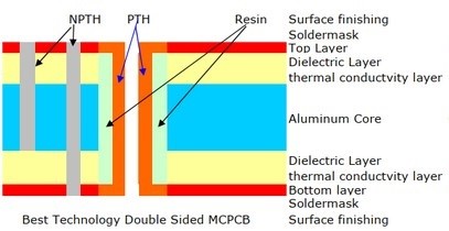
For a 2L MCPCB, the metal core is positioning on the bottom side of the MCPCB as a cooling carrier to the whole MCPCB, while the metal base of double sided MCPCB is located in the middle of two copper trace. In generally, some PTH (plated-through-hole) vias are needed to designed to connect the bottom and top traces.

Below are the stack ups of these two kinds of products, from the structure, we can easily distinguish which one is 2L MCPCB and which one is double sided MCPCB.

Heat dissipation of 2L MCPCB and Double Sided MCPCB

Due to the different structure of the two products, their heat dissipation performance is also different. The main reason is the heating of double-sided metal core circuits can be spread out through both top and bottom side, while the heating generate by SMD components of 2 layers circuit only can be dissipated through bottom (metal) side and the heat need to go down layer by layer. In addition to this, the dissipation of FR4 is not good than metal materials, so double-sided metal core printed circuits perform better heat dissipation performance than 2 layers MCPCB.

Surface mounted locations (SMD populate)

Nowadays, surface mounted technology (SMT) is widely used in printed circuit board industry, more and more designers prefer to populate electronic components of the circuit surface to achieve high density, stable electrical performance and high reliability. 2L metal core circuit boards and double-sided metal core circuits also show their different mounted locations in this aspect.

The populate location of a 2L MCPCB only available on copper trace side, that is top side. And a double-sided metal core PCB can mount components on both top and bottom side, because both of them exist copper trace on it.

Manufacturing technology

May somebody will curious about “Are these two products produced in the same process/technology?”

The answer is obvious “NO, they have a different laminate process when fabricating.”

Different with single layer MCPCB, double sided MCPCB requires an additional pressing step to laminate the thermal conductive layer and metal core together. But sometimes, some raw Metal Clad material vendor will supply board material which already laminated.

For 2 layers metal core PCB, due to it is made of a single MCPCB and a double-sided FR4 PCB, the first thing we should make a double sided FR4 PCB, then laminate the PCB together with the single MCPCB. But due to the thermal conductive layer (pure adhesive) is easy to overflow during laminating process, which will cause the poor adhesion and crack between metal core and FR4 PCB. In the meantime, to avoid such problem, an experienced operator is needed to proceed the laminated process. That is why the lead time and cost of a 2 layers metal core circuit is much longer and expensive.

This is the end of this post, if you still have some questions or difficulties about the metal core PCB, welcome to contact us at sales@bestpcbs.com, our professional sales team and engineering team will give you a best solution for free.

You may also like

What is the DBC Ceramic Copper Oxidation Technology

February 20th, 2023

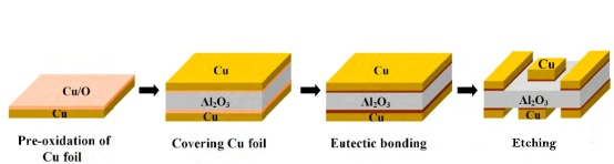
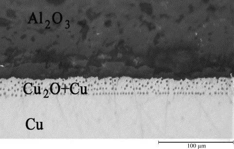
DBC (Direct Bond Copper) ceramic PCB also known as DCB ceramic, which is widely used in various type of high-power semiconductor, especially in IGBT package material by means of its excellent electricity and thermal conductivity of copper and the advantages of high mechanical strength and low dielectric loss of ceramics. DBC technology uses the oxygen-containing eutectic solution of copper to directly apply it to the ceramic. The key factor in the preparation process is the introduction of oxygen element, so the copper foil needs to be pre-oxidized in advance. Do you want to know what is the copper foil oxidation technology during the DBC ceramics manufacturing? Hereinbelow, we will introduce the oxidation process for you.
Oxidation technology of copper foil

Copper oxidation is divided into Wet Air Oxidation (including soaking oxidation and spraying oxidation) and Dry Oxidation.  Both oxidation methods can form CuO or Cu2O on the surface of copper foil.

  • Wet Air Oxidation (WAO)

i. Soaking oxidation

First, the copper is pickled with 3% dilute sulfuric acid, and then washed by the spray washing machine after overflow. Next, sent the copper into the mixed solution of potassium permanganate and copper sulfate (the concentration of potassium permanganate is about 31.6mg/L and the copper sulfate is about 95.4mg/L) for soaking and oxidation.  The oxidized copper is then washed with water and three-stage countercurrent washing, and then slowly pulled for dehydration and drying (the temperature is about 100℃) to complete soaking and oxidation.

ii. Spraying oxidation

Spraying oxidation is a kind of WAO, only the oxidation method become spraying. Spray oxidation is to spray copper with mixed solution of manganese nitrate and copper nitrate (concentration of about 3%) after pickling and washing.  The sprayed copper is dried directly in the tunnel kiln (the temperature is about 200℃).  In the drying process of tunnel kiln, the manganese nitrate and copper nitrate sprayed on the copper sheet are decomposed into copper oxide and manganese oxide.  The ratio of soaking oxidation and spraying oxidation treatment of copper sheet is about 5:5.

  • Dry Oxidation

Dry oxidation is very easy to process, put the copper into oxidation oven firstly, then heating up to 600~800oC for oxidizing around 30mins and then subjected to air cooling annealing.

Wet Air Oxidation VS Dry Oxidation

At present, the existing industry is widely used to finish the high-temperature annealing oxidation of copper then sintering with ceramic substrate, that is dry oxidation.  But this high temperature annealing, oxidation in one way has some drawbacks as following:

  1. Uneven oxidation. It will directly cause sintering defects during sintering, and the peeling strength will change greatly.
  2. Leaving conveyor belt marks.  Because the high temperature and oxidation process is transported by the conveyor belt, the existence of the conveyor belt mesh will affect the temperature distribution of the entire copper is not uniform, leaving marks/traces of the conveyor belt.  The result of sintering is to leave the corresponding trace on the bonding surface of CuAl2O3.
  3. High temperature annealing and oxidation will accompany the grain growth of copper. In the subsequent sintering process, the grain will continue to grow, which brings adverse effects on the mechanical properties and surface treatment of copper.  The copper surface grain produced by wet oxidation is fine, which is conducive to improving the mechanical properties of copper and eliminating the traces of conveyor belt. The main difference between wet oxidation and dry oxidation is shown in the bending resistance, heat resistance cycle performance and peeling strength, and these three indicators are significantly better than dry oxidation. Wet oxidation products can better meet the requirements of bending strength and heat resistance cycle performance.

So, this is the end of this post, EBest Circuit (Best Technology) specialized in fabricating ceramic PCB (including DBC, DPC, AMB, HTCC and LTCC technology) for more than 16 years, we have rich engineering team and professional sales team can provide one-stop service for you. Welcome to contact us if you have any inquiries about ceramic PCB.
You may also like