PCB manufacturing PCB manufacturing
Home > Blog

What Is a Surface Mount Device? Package, Footprint and Assembly Guide

July 15th, 2026

A surface mount device (SMD) is an electronic component designed to be soldered directly onto copper lands on the surface of a printed circuit board. Unlike a through-hole part, its terminals normally do not pass through plated holes. SMDs include chip resistors, capacitors, diodes, transistors, LEDs, sensors, connectors and integrated circuits.

The definition is simple, but selecting an SMD is also a manufacturing decision. The package must match the PCB footprint, polarity and pin-one data must agree across the schematic, BOM and pick-and-place file, and the assembly process must be able to print, place, reflow and inspect the resulting joints.

3D view of surface mount devices attached to copper pads on a populated PCB

What Is a Surface Mount Device?

A surface mount device is the physical electronic part that an SMT line places and solders onto PCB surface pads. Its electrical terminals may be metal end caps, gull-wing leads, J-leads, flat pads, exposed thermal pads or solder balls, depending on the package.

The term describes the mounting format, not the electrical function. A resistor, MOSFET, microcontroller and connector can all be SMDs even though they perform very different jobs. The common feature is that the package is intended for surface attachment and must be paired with a compatible PCB land pattern.

How Is an SMD Different from SMT and Through-Hole Components?

SMD is the component, SMT is the assembly technology, and through-hole describes parts whose leads are inserted through drilled holes. The terms are related but not interchangeable.

Term What It Means Main Design Concern
SMD The surface-mount component Package, pinout, polarity, thermal pad and availability
SMT The process used to assemble SMDs Solder paste, placement, reflow and inspection
Through-hole A component with leads inserted through PCB holes Hole size, annular ring, insertion and mechanical support

Many production PCBAs use mixed assembly. Small passives and ICs are commonly surface mounted, while some connectors, transformers, switches or mechanically loaded parts may remain through-hole. The correct choice depends on electrical, thermal, mechanical and service requirements rather than package size alone.

What Are the Common Surface Mount Device Package Types?

Common surface mount device package types range from two-terminal chip parts to fine-pitch and bottom-terminated ICs. The package name identifies a physical family, but the exact dimensions and pin mapping must still be confirmed in the manufacturer datasheet.

Common SMD package families shown beside their matching PCB land patterns and polarity marks
Package Family Typical Parts Assembly Attention
Chip packages such as 0402, 0603 and 0805 Resistors, capacitors and inductors Paste balance, placement accuracy and tombstoning risk
SOT and SOD Transistors, regulators and diodes Pinout and polarity or orientation marks
SOIC, TSSOP and QFP Integrated circuits Lead pitch, coplanarity, paste control and bridge inspection
QFN and DFN ICs and power devices Exposed-pad paste coverage and hidden perimeter joints
BGA and LGA Processors, memory and modules Land design, warpage, reflow control and X-ray inspection
PLCC and SMD LED packages LEDs and selected ICs Polarity, thermal path and optical orientation

A label such as 0603 can be ambiguous because imperial and metric naming systems use different dimensions. Put the manufacturer part number and package dimensions in the BOM instead of relying only on a short package code.

How Do You Match an SMD Package to a PCB Footprint?

Reliable SMD footprint design starts with the exact component datasheet and its recommended land pattern, not with a visually similar library name. Compare package body size, terminal dimensions, pitch, exposed-pad geometry, pin numbering and the datasheet revision before releasing the layout.

IPC-7351 provides generic requirements for surface-mount design and land patterns, including considerations for solder joints, inspection and rework. A generic standard does not replace a component-specific recommendation; use both where applicable and confirm the assembly supplier’s process capabilities.

  • Verify the manufacturer part number against the schematic symbol and BOM.
  • Check pad length, width, pitch and solder-mask clearances.
  • Confirm paste apertures for exposed pads and fine-pitch leads.
  • Keep a suitable component courtyard for placement, inspection and rework.
  • Check pin one, cathode, positive terminal and package rotation conventions.
  • Review thermal vias and copper spreading for power packages.

A footprint can be electrically correct yet difficult to manufacture. Large paste deposits may void or float a bottom-terminated package, undersized pads can reduce solder fillets, and crowded courtyards can block inspection or rework access.

Why Do SMD Polarity Markings and Orientation Matter?

SMD polarity markings and pin-one indicators prevent electrically asymmetric parts from being assembled in the wrong direction. Diodes, LEDs, polarized capacitors and most ICs require consistent orientation data, while ordinary resistors and many ceramic capacitors are non-polarized.

Do not assume every package uses the same dot, stripe, notch or chamfer convention. Read the component datasheet, then make the schematic symbol, PCB footprint, silkscreen, assembly drawing and centroid rotation agree. The BOM should identify the exact manufacturer part number so an alternate package is not substituted without review.

Before fabrication, compare a top-view package drawing with the top-view PCB footprint. This simple check catches mirrored footprints, transposed pins and ambiguous polarity marks before they become an assembled-board failure.

How Does Surface Mount Device Assembly Work?

Surface mount device assembly normally follows solder paste printing, automated placement, controlled reflow and inspection. Each stage depends on correct design data from the previous stage.

SMT line showing solder paste printing, SMD placement and reflow soldering
  1. A laser-cut stencil deposits solder paste on the PCB pads.
  2. Feeders present parts from reels, tubes or trays to the placement machine.
  3. Pick-and-place nozzles identify, orient and place each SMD from centroid data.
  4. The reflow oven heats the assembly according to the solder paste and component limits.
  5. AOI checks visible placement and solder-joint conditions.
  6. X-ray inspection may be used for BGA, QFN, LGA and other hidden joints.
  7. Electrical or functional testing checks whether the assembled circuit operates as required.

BestPCBs provides PCB assembly and PCBA support that includes component sourcing, SMT and mixed assembly, inspection and testing. If paste volume requires special control, the related SMT stencil service can support framed, unframed and stepped stencil requirements.

Which Files Are Needed for SMD PCB Assembly?

A manufacturer needs synchronized design and purchasing data to assemble SMDs correctly. At minimum, prepare fabrication data, a BOM, centroid or pick-and-place data and an assembly drawing.

  • Gerber or ODB++ files for PCB fabrication
  • BOM with manufacturer part number, description, quantity and package
  • Pick-and-place file with reference designator, X/Y location, side and rotation
  • Assembly drawing with pin-one and polarity information
  • Stencil or paste-layer data
  • Approved alternates and do-not-substitute restrictions
  • Programming, test and special handling instructions

Run a cross-check before quotation: every placed reference designator should exist in the BOM, every BOM line should map to the intended footprint, and every polarized part should have an unambiguous orientation. The custom PCB assembly checklist provides a broader handoff path for prototype and production builds.

What Surface Mount Device Quality Problems Should You Check?

Common SMD assembly problems include wrong parts, reversed polarity, component shift, tombstoning, solder bridges, insufficient solder, open joints and hidden-joint voiding. Inspection should be selected according to the package and the visibility of its connections.

AOI and X-ray inspection of visible and hidden solder joints on a surface mount PCB assembly
Risk Typical Check Design or Process Response
Wrong or reversed component BOM verification, AOI and functional test Clear part number, polarity and rotation data
Tombstoned chip component AOI or visual inspection Balanced pads, paste deposits and thermal conditions
Bridged fine-pitch leads AOI and electrical test Review land pattern, stencil aperture and reflow process
Open or insufficient joint AOI, visual inspection or electrical test Check paste transfer, coplanarity and wetting surfaces
Hidden BGA or QFN concern X-ray and functional test Review pad geometry, paste segmentation and reflow profile

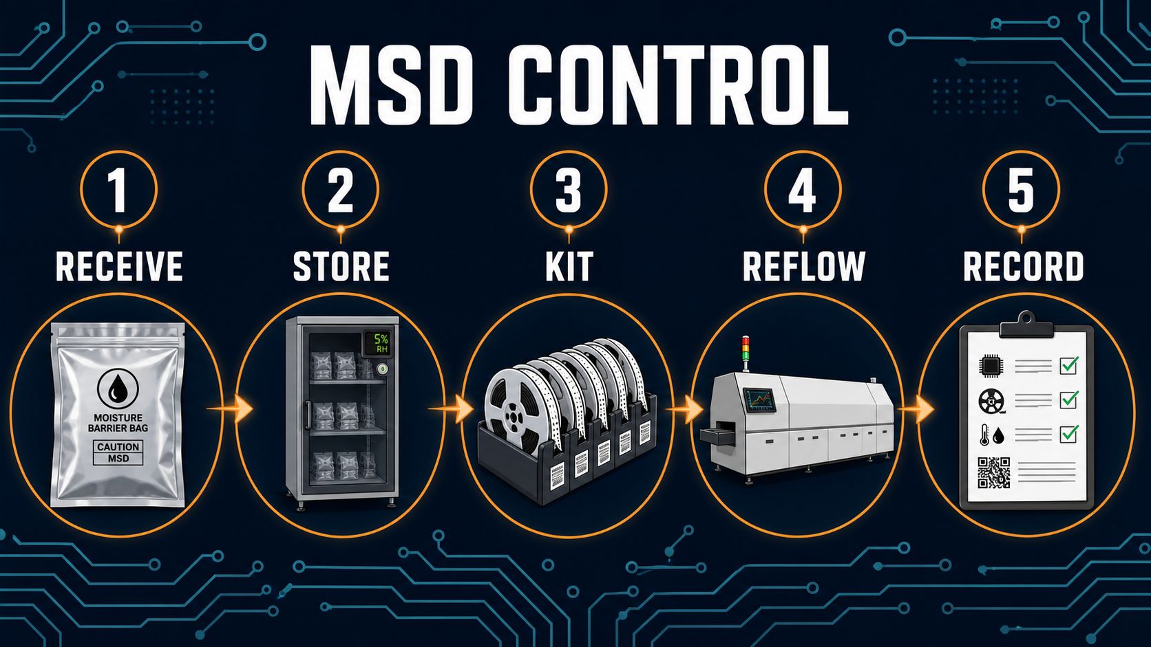
Moisture-sensitive semiconductor packages also need controlled storage and floor-life handling. Moisture trapped inside a package can expand during reflow and cause internal damage; check the component’s moisture sensitivity level, packaging label and applicable handling instructions before assembly.

How Do You Choose a Surface Mount Device for Production?

The best production choice is the SMD that meets electrical requirements while remaining available, inspectable and compatible with the intended assembly process. The smallest package is not automatically the lowest-risk or lowest-cost option.

  • Electrical: voltage, current, tolerance, frequency, leakage and noise.
  • Thermal: power dissipation, junction temperature, exposed pad and PCB heat path.
  • Mechanical: package dimensions, board flex, vibration and connector loading.
  • Manufacturing: pitch, stencil release, placement accuracy, rework and inspection access.
  • Supply chain: lifecycle status, approved sources, lead time and qualified alternates.
  • Documentation: reliable datasheet, land pattern, 3D model and traceable part number.

For an early prototype, a slightly larger leaded package may reduce hand-assembly and rework difficulty. For volume production, a smaller bottom-terminated package may save area and improve electrical or thermal performance, but it can require tighter paste control and X-ray access. Review the trade-off with the assembler before freezing the layout.

Frequently Asked Questions About Surface Mount Devices

Are all SMD components polarized?
No. Resistors and many ceramic capacitors are non-polarized. Diodes, LEDs, polarized capacitors and most integrated circuits require a defined orientation. Always use the datasheet rather than guessing from package shape.

Can a surface mount device be soldered by hand?
Many larger SMD packages can be hand-soldered for prototypes or repair with suitable tools and magnification. Fine-pitch, bottom-terminated and very small packages are more repeatable with controlled paste printing, placement and reflow.

What does 0603 mean on an SMD package?
It is a size code, but it can refer to different dimensions in imperial and metric systems. Confirm the actual body dimensions in the component datasheet and state the full manufacturer part number in the BOM.

Does an SMD need drilled component holes?
Normally no. Its terminals attach to surface lands. A PCB can still contain vias, tooling holes and through-hole parts elsewhere, and some special surface-mount packages include mechanical locating features.

Are QFN and BGA components SMDs?
Yes. Both are surface-mount package families. Their solder joints are partly or fully underneath the body, so land design, paste control, reflow and X-ray inspection deserve special attention.

Can two components with the same value use different footprints?
Yes. The same electrical value can be sold in multiple package sizes and pin configurations. A substitute is acceptable only when electrical ratings, package dimensions, pinout, thermal behavior and manufacturing constraints are all compatible.

Why are many SMDs supplied on tape and reel?
Tape-and-reel packaging protects component orientation and lets automated feeders present parts consistently to a pick-and-place machine. Tubes and trays are also common for larger or specialized packages.

What is MSL for a surface mount device?
Moisture Sensitivity Level defines handling precautions and allowable exposure conditions for moisture-sensitive packages before reflow. Follow the package label, manufacturer guidance and the applicable handling standard.

Which inspection method is used for SMD solder joints?
AOI is useful for visible placement and joint conditions. X-ray is commonly considered for hidden joints under BGA, QFN and similar packages. Electrical and functional tests confirm circuit behavior that visual inspection cannot prove.

What should be checked before approving an SMD alternate?
Check function, ratings, pinout, package dimensions, land-pattern compatibility, polarity, thermal needs, lifecycle status and assembly implications. Document the approved alternate in the BOM instead of allowing an uncontrolled substitution.

Summary

A surface mount device is a component made for direct attachment to PCB surface lands, but a production-ready choice requires more than identifying an SMD package. Match the exact part to its footprint, control orientation and moisture handling, provide synchronized assembly files, and plan inspection around visible or hidden solder joints.

If you are preparing a surface mount device assembly project, send your Gerber files, BOM, pick-and-place data, quantity and test requirements to sales@bestpcbs.com. The EBest Circuit engineering team can review the package-to-footprint handoff and provide a PCB/PCBA manufacturing quotation.

You may also like

Capped Via Guide: Filled Vias, IPC-4761 Type VII and DFM Checks

July 15th, 2026

A capped via is a PCB via that is filled and then plated or capped over to create a sealed, flatter surface. It is often used when a via must be protected from solder wicking, contamination, voiding, or surface irregularity in dense PCB layouts.

For engineers and buyers, capped vias are not just a drawing detail. They affect manufacturability, inspection, cost, reliability, and how clearly the fabrication notes must be written before production.

Cross-section illustration of filled and capped vias in a multilayer PCB
Filled and capped vias create a sealed surface that helps reduce solder wicking and surface irregularity.

What Is a Capped Via?

A capped via is a via hole that has been filled and then covered with copper plating or another specified cap structure.

In PCB manufacturing, vias connect copper layers through the board. A standard via may remain open, while a tented, plugged, filled, or capped via receives additional processing. A capped via usually provides a more protected surface than simple solder mask tenting, especially when the board has dense routing, fine-pitch parts, or via-in-pad requirements.

If you are comparing different via protection options, this related guide on tented via, filled via, and plugged via can help clarify the basic differences.

Comparison of open via and capped via structures in a multilayer PCB
Open vias leave the hole exposed, while capped vias use fill and cap plating to close the surface.

Why Are Capped Vias Used in PCB Manufacturing?

Capped vias are used to improve surface reliability, reduce solder-related problems, and support compact PCB layouts where ordinary open vias may create risk.

  • They can help prevent solder from flowing into via holes during assembly.
  • They can reduce contamination traps in exposed via openings.
  • They can support smoother pad or surface areas when required by the layout.
  • They can improve process control for high-density and reliability-focused PCB builds.

Capped vias are common in more complex products, including HDI PCB projects, dense BGA areas, compact control boards, and high-reliability electronics.

How Does the Capped Via Process Work?

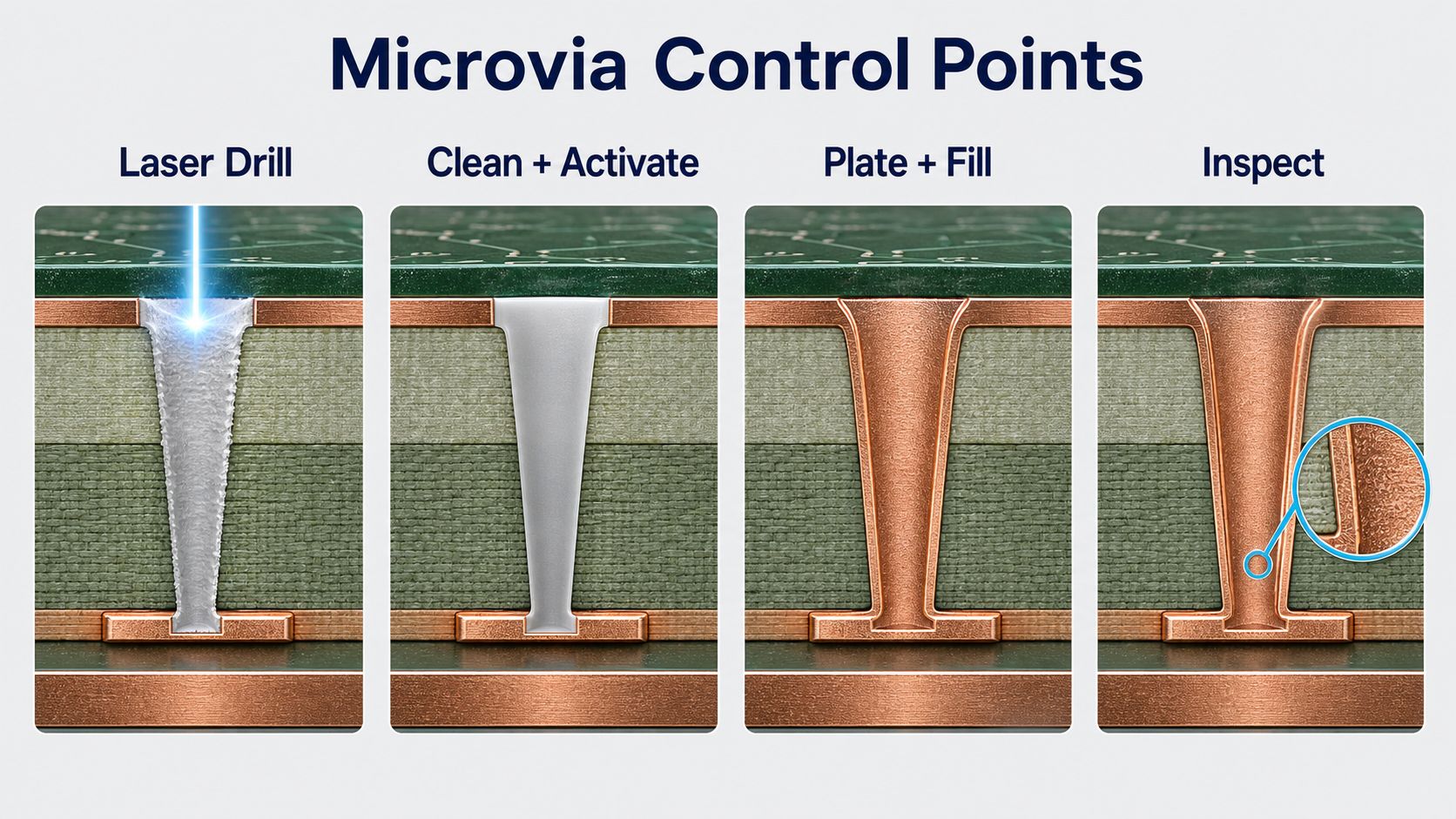
The capped via process usually includes drilling, plating, filling, curing, planarization, cap plating, and inspection.

Step Purpose
Drilling Create the via hole.
Plating Form the conductive barrel.
Filling Fill the via with specified material.
Curing Stabilize the fill material.
Planarization Flatten excess material.
Cap plating Cover the filled via surface.
Inspection Check filling, cap quality, and surface condition.

For quality verification, a PCB cross section may be used to inspect via filling, plating, barrel condition, and cap structure when the project requires deeper validation.

What Is the Difference Between Filled and Capped Vias?

Filled vias focus on filling the hole, while capped vias add a covered surface after the via is filled.

Via Type Main Feature Typical Use
Filled via Via hole is filled. Reduce voids or support reliability needs.
Filled and capped via Filled via is covered by cap plating. Improve surface condition and solder control.
Tented via Solder mask covers the via opening. Basic protection for suitable designs.
Plugged via Via is plugged but not necessarily fully capped. Cost-sensitive via protection.
Comparison of filled via, filled and capped via, tented via, and plugged via
Common via protection options include filled, capped, tented, and plugged vias.

When Should You Choose Epoxy Filled and Capped Vias?

Epoxy filled and capped vias are useful when the via structure needs added protection, improved surface quality, or better assembly reliability.

This option may be considered for via-in-pad structures, BGA fanout areas, dense routing, boards with strict solderability needs, or applications where open via holes may create contamination or solder wicking concerns. The exact choice should be reviewed during DFM because cost and process complexity are higher than basic via tenting.

How Does IPC-4761 Type VII Define Filled and Capped Vias?

IPC-4761 Type VII is commonly referenced for filled and capped via structures, where the via is filled and then covered.

When a drawing or fabrication note calls out IPC-4761 Type VII filled and capped vias, the PCB supplier should understand the intended via protection level. Buyers should still confirm the exact fill material, plating expectation, acceptance criteria, inspection method, and whether the requirement applies to all vias or only selected vias.

Capped Via vs Via Capping: Are They the Same?

Capped via usually refers to the final via structure, while via capping refers to the process or requirement of covering a filled via.

In many engineering conversations, the terms overlap. However, fabrication notes should avoid vague wording. Instead of simply writing “cap vias,” it is better to specify whether the board needs filled and capped vias, which vias are included, whether IPC-4761 Type VII applies, and what inspection requirement is expected.

What PCB Design and Manufacturing Issues Can Capped Vias Help Prevent?

Capped vias can help reduce solder wicking, trapped residues, surface unevenness, and reliability concerns in dense PCB areas.

They are often discussed during PCB design for manufacturing review because the right via protection method depends on pad location, via size, solder mask strategy, surface finish, assembly process, and inspection needs.

For specialized boards that combine unusual material, thickness, copper, or via requirements, a special PCB manufacturing review can help confirm whether capped vias are appropriate.

How Should You Specify Capped Vias in PCB Fabrication Files?

Capped vias should be specified clearly in fabrication notes, stackup files, drill tables, and drawings so the supplier knows exactly which vias need the process.

  • State whether the requirement is filled and capped via or another via covering type.
  • Identify which via sizes or locations require capping.
  • Call out IPC-4761 Type VII only when that is the intended structure.
  • Define whether the requirement applies to via-in-pad areas, BGA areas, or all vias.
  • Confirm inspection expectations before production.

If the instruction is unclear, the supplier may quote the wrong process or ask for clarification, which can delay the project.

FAQs about Capped Via

Is a capped via the same as a filled via?

No. A filled via means the hole is filled. A capped via normally means the filled via is also covered by a cap or plating layer.

Is via capping always required for via-in-pad?

Not always, but via-in-pad designs often require filled and capped vias to prevent solder loss and surface problems during assembly.

Does IPC-4761 Type VII mean filled and capped vias?

Yes, IPC-4761 Type VII is commonly used to describe filled and capped via protection. The exact fabrication note should still be reviewed with the PCB supplier.

Are capped vias more expensive?

Yes. Capped vias add filling, curing, planarization, plating, and inspection steps, so they usually cost more than standard open or tented vias.

What should I send for a capped via quote?

Send Gerber or ODB++ files, drill files, stackup, via table, fabrication notes, IPC requirement, surface finish, quantity, lead time, and inspection expectations.

In Conclusion, a capped via can improve PCB manufacturability and assembly reliability when the board needs protected, filled, and plated via structures. To avoid quotation mistakes, specify the via type clearly, review IPC-4761 Type VII requirements carefully, and confirm the process with your PCB manufacturer before production.

EBest Circuit (Best Technology) supports PCB manufacturing, DFM review, PCB layout manufacturability review, component sourcing, PCBA assembly, and testing support. If you need help reviewing capped via requirements for a PCB or PCBA project, contact the engineering team at sales@bestpcbs.com.

You may also like

PCB Manufacturing Energy Consumption and Embodied Energy

July 15th, 2026

PCB manufacturing energy consumption is the electricity, heat, process energy, material energy, and indirect supply-chain impact needed to turn laminate, copper, chemistry, tooling, and design data into a finished printed circuit board. For most buyers, the useful question is not a single universal kWh number. It is which board decisions, fabrication steps, supplier controls, and quote details can reduce unnecessary energy, scrap, rework, and embodied carbon without weakening reliability.

PCB manufacturing energy consumption in a fabrication process

Public PCB life-cycle and decarbonization research generally points in the same direction: board impact depends on materials, fabrication energy, chemicals, yield loss, transport, assembly, use phase, and end-of-life treatment. Those inputs vary sharply by stackup and process. A simple two-layer FR-4 board, a high-layer-count HDI board, a metal-core thermal board, and an automotive ceramic substrate do not carry the same manufacturing burden.

What PCB Manufacturing Energy Consumption Means

PCB manufacturing energy consumption means the energy used directly in fabrication plus the upstream energy already embedded in materials such as copper foil, laminate, prepreg, solder mask, surface finish chemistry, and packaging. In practical sourcing, it is better to treat this as a decision map than as a fixed number.

A buyer can influence energy-related impact before the order reaches the factory. Layer count, board size, copper weight, via structure, impedance tolerance, surface finish, acceptance criteria, and panel utilization all affect how many process steps the board needs. A supplier can influence the same outcome through process control, first-pass yield, waste handling, equipment efficiency, and transparent data collection.

Where Energy and Carbon Impact Enter the PCB Life Cycle

Energy enters the PCB life cycle through raw materials, fabrication, assembly, transport, product use, rework, and disposal or recycling. A quote that only compares unit price can miss several of these drivers.

Life-cycle stage Typical energy or carbon driver Buyer check
Material production Copper, glass fiber, resin, ceramic, aluminum or specialty laminate production Ask whether the requested material is necessary for the electrical, thermal, or mechanical requirement.
PCB fabrication Imaging, etching, lamination, drilling, plating, solder mask, surface finish, routing and testing Confirm which process steps are driven by the stackup and tolerance choices.
Assembly Stencil printing, placement, reflow, inspection, cleaning, selective soldering, test fixtures Separate bare-board and PCBA requirements in the RFQ.
Yield and rework Scrap panels, rejected boards, rework loops and repeated testing Provide complete files and request DFM review before production release.
Logistics Shipment mode, partial shipments, urgent reorders and packaging Plan quantities and approval steps early enough to avoid emergency freight.

Which PCB Design Choices Usually Affect Energy Use

The design choices most likely to change manufacturing energy are layer count, board area, copper thickness, via structure, controlled impedance, surface finish, and tolerance tightness. Each one can add process complexity when it goes beyond what the design actually needs.

Layer count is often the first lever. Extra layers may be necessary for routing density, EMI control, power integrity, or controlled impedance, but they also add lamination, imaging, inspection, and material demand. Board size and panel utilization matter as well. A shape that wastes panel area can increase scrap even when the finished board is small.

Copper thickness affects etching and plating. Via structures affect drilling, desmear, plating, filling, capping, and inspection steps. Surface finish should match assembly and storage needs rather than habit. If the project only needs standard solderability, an expensive or process-heavy finish may not be justified.

How Fabrication Steps Influence Energy Consumption

Fabrication energy is distributed across repeated wet processing, lamination, drilling, plating, baking, inspection, routing, and testing steps. The more times a board must pass through those steps, the more important process discipline becomes.

For example, a multilayer board may require inner-layer imaging and etching before layup, then lamination, drilling, copper plating, outer-layer imaging, solder mask, surface finish, profiling, electrical test, and final inspection. An HDI design can add laser drilling, microvia plating, sequential lamination, via filling, and tighter inspection. These process choices may be technically correct, but they should be tied to a real electrical or reliability need.

For a plain-language explanation of how stackup and process complexity interact, see our guide to multilayer PCB manufacturing.

Why Yield, Scrap, and Rework Matter

Yield is one of the most overlooked energy variables because every scrapped board carries the material and process energy already spent on it. Lower yield can turn a technically efficient process into a wasteful one.

Many yield problems start before fabrication: missing drill files, unclear stackup notes, ambiguous copper requirements, insufficient annular ring, unsupported solder mask slivers, unrealistic impedance tolerances, and mismatch between BOM, CPL, and drawings for PCBA orders. A proper DFM review reduces the chance of re-running panels, remaking tooling, or holding production while questions are resolved.

For buyers comparing fabrication plus assembly scope, the distinction between a bare PCB and a fully assembled PCBA also matters. The article PCB vs PCBA explains where the manufacturing boundary changes.

How Materials and Layer Count Change Embodied Energy

Embodied energy changes when a board uses more material, harder-to-process material, tighter reliability requirements, or a stackup that needs extra lamination and inspection. A lightweight design is not automatically lower impact if it causes poor yield or field failure.

FR-4, high-Tg FR-4, low-loss RF laminate, metal-core materials, ceramic substrates, heavy copper, and rigid-flex constructions solve different engineering problems. The lower-impact choice is the material that satisfies the product requirement with the least avoidable complexity. For thermal products, that may mean using a metal-core or ceramic option only where the heat path demands it. For high-speed products, it may mean choosing a stable laminate and stackup early so the factory does not need repeated trial builds.

Cost and sustainability often meet in the same place: avoid over-specification, avoid unclear files, and avoid rework. Our custom PCB cost guide covers many of the same quote variables from a price perspective.

What Buyers Can Ask Before Requesting a PCB Quote

The best RFQ questions focus on data quality, process fit, yield protection, and whether the supplier can explain tradeoffs instead of making vague carbon claims. Most buyers do not need a perfect carbon model for every board; they need better decisions before production starts.

  • Can the supplier review stackup, material, copper weight, via type, tolerance and finish before quoting final production?
  • Which requested features are driving extra lamination, plating, drilling, testing or inspection steps?
  • Can panel utilization be improved without changing the finished board outline?
  • Are any tolerances tighter than the product actually needs?
  • Will the quote separate bare-board fabrication, assembly, testing, tooling, freight and rework risk?
  • Can the supplier flag file issues that may cause scrap before mass production?

How to Compare Suppliers Without Unverified Carbon Claims

Compare suppliers by the quality of their manufacturing data and engineering review, not by unsupported ?green PCB? marketing language. If a supplier gives a carbon or energy figure, ask what scope, boundary, method, and board assumptions it uses.

A useful comparison should state whether it covers material production, board fabrication, assembly, transport, use phase, and end-of-life. It should also clarify whether the data is plant-level, product-level, estimate-based, or supplier-reported. Without those boundaries, two numbers may look comparable while measuring different things.

For online sourcing workflows, the file package still matters. Our article on choosing a PCB manufacturer online lists the documents that help a supplier quote and review the board properly.

Practical Design Checks for Lower-Impact PCB Sourcing

The most practical way to lower unnecessary impact is to design for manufacturability, avoid avoidable complexity, and give the supplier enough information to build the board right the first time. The same habits usually reduce lead-time risk and cost.

  1. Confirm that layer count and stackup are needed for the signal, power, thermal, and mechanical requirements.
  2. Use the simplest via structure that still meets density and reliability needs.
  3. Choose copper weight based on current, thermal rise, and manufacturability, not guesswork.
  4. Match surface finish to assembly, storage, wire bonding, or contact requirements.
  5. Review panelization early when the board outline is unusual.
  6. Run DFM review before freezing production quantity.
  7. Separate prototype learning builds from production release builds.

If your project includes assembly or component sourcing, include BOM and placement files at the same time as Gerber or ODB++ data. The PCBA service page explains the broader manufacturing scope beyond bare-board fabrication.

FAQ About PCB Manufacturing Energy Consumption

These questions come up when engineering teams start connecting PCB sourcing with carbon, cost, and manufacturing reliability.

Is there one standard energy number for PCB manufacturing?

No. Energy depends on board size, layer count, material, copper weight, via structure, surface finish, process route, yield, test scope, and factory energy mix. A single number without board assumptions is not useful for sourcing.

Does fewer layers always mean lower embodied energy?

Usually fewer layers reduce material and process complexity, but not always. If forcing fewer layers causes poor routing, EMI problems, rework, or field failure, the lower layer count may create more waste over the product life.

Can DFM review reduce PCB energy consumption?

DFM review can reduce avoidable scrap, repeated tooling, rework, and production holds. It does not magically make a board low-carbon, but it helps prevent waste caused by unclear or difficult-to-build designs.

Should buyers ask PCB suppliers for carbon data?

Yes, when the project requires sustainability reporting. Ask for the boundary and method behind the data. A plant-level or estimate-based value should not be treated the same as a product-specific life-cycle calculation.

Final RFQ Checklist for Energy-Aware PCB Projects

For an energy-aware PCB quote, send the same files needed for a reliable build, plus any sustainability reporting requirements you must meet. The goal is practical clarity, not green decoration.

  • Gerber or ODB++ files.
  • Stackup request, material preference, copper weight, impedance and thickness targets.
  • Surface finish, solder mask, silkscreen and special process requirements.
  • Quantity, prototype or production intent, and target lead time.
  • BOM, CPL, assembly drawing and test requirements if PCBA is included.
  • Any carbon, lifecycle, material declaration, RoHS/REACH or supplier reporting requirement.
  • Known design risks where DFM review is needed before release.

If you want a practical review before committing to production, send your Gerber or ODB++ files, BOM, CPL, quantity, material choice, surface finish, testing requirements, target lead time, and any sustainability reporting requirement to sales@bestpcbs.com. Our team can review the manufacturing route, flag avoidable complexity, and help you prepare a quote package that supports both reliability and lower-waste sourcing.

You may also like

PCB Manufacturer Online: Quote Files, DFM Checks and Ordering Risks

July 15th, 2026

A PCB manufacturer online can help you move from design files to a price request faster, but the safest quote still depends on complete manufacturing data, clear assembly scope, and a DFM review before release. Uploading Gerbers is only the start. Buyers also need drill files, stackup notes, quantity, material, surface finish, testing requirements, and, for PCBA, BOM and CPL data.

Use online PCB manufacturing as a fast RFQ channel, not as a substitute for engineering judgment. If the board has tight tolerances, impedance, special materials, heavy copper, HDI, flex sections, controlled testing, or component sourcing risk, ask the supplier to review the files before you treat the first price as final.

PCB manufacturer online quote preparation with Gerber files BOM and circuit boards
Online PCB quotes work best when the Gerber, drill, stackup, BOM, CPL, quantity, material, finish, and test requirements are ready before upload.

What Does a PCB Manufacturer Online Actually Provide?

A PCB manufacturer online usually provides a digital way to submit PCB files, select specifications, request pricing, communicate requirements, and start fabrication or assembly review.

For simple prototype boards, that may be enough to get a quick estimate. For production or engineering-critical work, the online path should still connect to real manufacturing review. The important question is not only whether a website accepts files. The useful question is whether the supplier can catch missing information before the board reaches fabrication.

Online function What it helps with What still needs review
File submission Gerber, drill, ODB++, drawings, BOM, CPL Missing layers, naming errors, stackup mismatch
Quote request Quantity, board size, copper, finish, delivery target Special process, material availability, test scope
Order communication Questions, engineering notes, delivery details DFM exceptions, substitutions, approval records

Online PCB Manufacturer vs Engineering-Led RFQ

An online PCB quote is best for speed, while an engineering-led RFQ is better when the board has design, process, assembly, sourcing, or reliability risk.

Many searches for a PCB manufacturer online are driven by convenience. Buyers want a price without several email rounds. That is reasonable for a simple two-layer prototype. It becomes risky when the board has impedance control, fine-pitch parts, unusual materials, via-in-pad, tight mechanical fit, thermal stress, or production testing needs.

BestPCBs provides an online enquiry path for PCB and PCBA projects. Treat it as a structured RFQ entry point: send complete files, then let the engineering and sales team confirm manufacturability, assembly scope, and quotation details.

Files You Need Before Requesting an Online PCB Quote

The fastest online PCB quote is the one that starts with a complete file package, because missing files create engineering questions and price changes later.

  • Gerber or ODB++ fabrication files with all copper, solder mask, paste, legend, outline, and mechanical layers.
  • NC drill files, drill map, slot notes, and plated/non-plated hole definitions.
  • Stackup, finished thickness, copper weight, material preference, impedance notes, and tolerance requirements.
  • Surface finish, solder mask color, silkscreen color, panelization preference, and testing requirements.
  • For assembly: BOM, CPL or pick-and-place file, assembly drawing, polarity notes, approved alternates, and functional test plan.

If you are not sure whether you need bare PCB fabrication or complete assembly, compare the sourcing path in this PCB vs PCBA guide before you request pricing.

What Instant PCB Quotes Can Calculate Well

Instant PCB quote tools are useful for standard specifications that can be priced from clear inputs such as size, layers, quantity, thickness, copper, solder mask, finish, and delivery target.

These tools can give a reasonable starting point when the design fits normal fabrication rules. They are especially useful for early budget comparisons, prototype planning, and checking how quantity or lead time changes the price.

Input Usually easy to price online Needs confirmation when
Board size and quantity Panel area and batch cost Outline is irregular or panelization is constrained
Layer count and thickness Standard stackups Impedance or special dielectric is required
Surface finish Common finish options Special reliability or shelf-life requirement exists
Assembly quantity Placement count and basic labor BOM availability or substitutes are uncertain

What Online PCB Quote Tools Often Miss

Online quote tools often miss the engineering details that change manufacturability, yield, component sourcing, test method, or final delivery risk.

A price form may not understand whether a trace runs too close to the board edge, whether a connector area needs mechanical support, whether a component is obsolete, or whether a test point is reachable after assembly. These are not small details. They can decide whether the first build ships on time or turns into a rework discussion.

For a deeper look at price drivers, use the custom PCB cost guide together with your online quote comparison.

How to Compare PCB Manufacturer Online Options

Compare online PCB manufacturers by engineering response, file review, material clarity, assembly support, testing options, communication, and delivery reliability, not price alone.

  • Does the supplier review Gerber, drill, stackup, and drawing data before release?
  • Can they quote both bare PCB and PCBA manufacturing when the project needs assembly?
  • Do they ask for test requirements instead of assuming only basic electrical test?
  • Can they explain price changes when a design moves from prototype to repeat production?
  • Do they provide a clear communication path if a file, material, or BOM issue appears?

Bare PCB, PCBA, and Turnkey Quote Differences

Bare PCB quotes cover the board only; PCBA quotes add component mounting; turnkey quotes also include component sourcing, assembly, inspection, and sometimes functional testing.

Confusing these scopes is a common online ordering mistake. A bare board price may look low because it excludes components, stencil, placement, inspection, and test. A PCBA quote may change after BOM review if parts are unavailable, package data is unclear, or approved alternates are missing.

If the project needs parts procurement, include sourcing expectations early and review the component sourcing service path before you compare suppliers.

DFM Checks Before You Upload Gerbers

A quick DFM check before upload reduces quote delays because the manufacturer receives files that are easier to review and price accurately.

  • Confirm board outline, slots, cutouts, and mechanical dimensions match the drawing.
  • Check minimum trace, spacing, annular ring, drill size, and solder mask clearance against the intended supplier route.
  • Verify layer order, copper weights, impedance notes, and controlled-depth or special drill instructions.
  • For assembly, check polarity marks, part rotation, footprint fit, test points, and connector orientation.
  • Remove conflicting notes from old revisions before sending the RFQ package.

The older PCB manufacturing process page can help buyers understand why each fabrication step needs clean input data.

Cost Factors That Change After Engineering Review

PCB cost can change after engineering review when the original online inputs miss material choice, tolerance, special process, assembly complexity, component availability, testing, or schedule pressure.

Cost driver Why it changes after review How to reduce surprise
Material Selected material may not match electrical, thermal, or availability needs Send material preference and acceptable alternatives
Drill and copper rules Tight features may require a different process route Confirm design rules before final layout release
Assembly Fine-pitch parts, BGAs, odd shapes, or hand operations change labor and inspection Send BOM, CPL, drawings, and photos if available
Testing Functional test, fixture needs, or special inspection may not be included State test requirements in the first RFQ

Lead Time, Shipping, and Communication Risks

Online ordering can shorten the quote cycle, but lead time still depends on complete files, material availability, engineering questions, production load, testing scope, and shipping route.

Do not compare two online quotes only by the number shown beside delivery. Ask whether the time starts after payment, after file approval, after engineering questions are cleared, or after components arrive. For assembled boards, component sourcing can easily become the pacing item.

Prototype assemblies often need a different planning rhythm from production builds; the prototype PCB assembly page is a useful reference when the goal is a fast engineering build.

Red Flags Before Placing an Online PCB Order

Red flags include a quote that ignores missing files, accepts unclear stackups, does not ask about test requirements, hides assembly exclusions, or cannot explain what happens when DFM issues appear.

  • The supplier gives a final-looking price from screenshots instead of manufacturing files.
  • The quote form has no place for drawings, tolerance notes, testing, or assembly requirements.
  • The BOM review does not mention lifecycle, package, substitute, or sourcing risk.
  • Delivery timing is advertised but not tied to engineering approval or component arrival.
  • Support cannot explain what happens if the Gerber and drawing disagree.

When to Ask for Manual Engineering Review

Ask for manual engineering review when the PCB has controlled impedance, HDI, heavy copper, flex or rigid-flex areas, high temperature, RF behavior, fine-pitch assembly, special testing, or production reliability requirements.

Manual review does not slow a serious project down; it prevents hidden problems from reaching production. A good supplier should be willing to review your files, explain unclear points, and confirm the quote scope before release.

Frequently Asked Questions About Online PCB Manufacturers

Can I get a reliable PCB quote online without talking to an engineer?

For simple prototypes, sometimes yes. For production, assembly, controlled impedance, unusual materials, or tight mechanical requirements, engineering review is safer before you approve the price.

What files should I upload for a PCB manufacturer online?

Upload Gerber or ODB++, drill files, stackup notes, material and finish requirements, quantity, test requirements, and, for PCBA, BOM, CPL, assembly drawings, and approved alternates.

Why does an online PCB price change after review?

The first price may not include missing process details, special materials, assembly difficulty, component sourcing risk, test fixtures, or delivery constraints.

Is the cheapest online PCB manufacturer always the best choice?

No. The lowest price is useful only when the quote scope, files, testing, delivery terms, and quality expectations are the same.

Final RFQ Checklist

Before choosing a PCB manufacturer online, prepare the complete file package and ask for review of the items that can affect quality, cost, and schedule.

  • Gerber or ODB++, NC drill, board outline, stackup, material, copper, finish, and quantity.
  • BOM, CPL, assembly drawing, polarity notes, approved alternates, and test plan for PCBA.
  • Target lead time, delivery address, packaging needs, and any reliability or inspection requirement.
  • Clear note if the quote is for prototype, pilot run, repeat production, or long-term sourcing.

If you want BestPCBs to review your project before quotation, send your Gerber or ODB++ files, drill files, stackup, BOM, CPL, quantity, material, surface finish, test requirements, and target delivery date through the online enquiry page or email sales@bestpcbs.com. The more complete the file package is, the faster the team can confirm manufacturability, assembly scope, sourcing risks, and quote details.

You may also like

Desoldering Gun for PCB Rework: Selection, Temperature, and Safe Use

July 15th, 2026

A desoldering gun combines a heated hollow nozzle with vacuum suction, allowing an operator to melt and remove solder from a plated through-hole joint in one controlled action. It is faster and more repeatable than switching between a soldering iron and a manual pump, but the result still depends on nozzle fit, heat transfer, suction timing, board support, and maintenance.

This desoldering gun guide explains how to select the right tool, set a sensible starting temperature, remove components without lifting pads, and inspect the PCB before installing a replacement. The focus is practical PCB rework rather than brand rankings.

Cutaway view of an electric vacuum desoldering gun removing solder from a through-hole PCB joint

What Is a Desoldering Gun and How Does It Work?

A desoldering gun heats the solder joint through a metal nozzle and then pulls the molten solder through the nozzle into a collection chamber. In an electric vacuum desoldering gun, the heater and suction path are integrated into the handpiece, so the nozzle can remain centered over the component lead while the pump is triggered.

The nozzle must transfer enough heat to melt solder throughout the plated barrel, not only on the surface pad. Once the solder is fully liquid, vacuum flow carries it through the nozzle. A filter traps solder and flux residue before they reach the pump. If the solder has not melted completely, stronger suction will not solve the problem; it may instead cool the joint and prolong heating.

This method is best suited to leaded parts such as connectors, relays, electrolytic capacitors, transformers, switches, and pin headers. Readers unfamiliar with these joints can first review how through-hole technology differs from SMT.

Desoldering Tool Types: Manual Pump, Electric Vacuum, and Hot Air

The best desoldering method depends on the component package, repair volume, and risk of thermal damage. A vacuum desoldering gun is usually the most efficient choice for repeated through-hole rework, while a manual pump is economical for occasional joints and hot air is generally better for surface-mount packages.

Manual solder sucker, electric vacuum desoldering gun, and hot-air rework handpiece shown with suitable PCB joints

Tool type Best use Main advantage Main limitation
Manual solder sucker plus iron Occasional single-sided or simple through-hole repair Low cost and easy portability Heat and suction occur as separate actions, which can leave solder in the barrel
Electric vacuum desoldering gun Repeated through-hole PCB rework Integrated heating and suction with better control around the lead Requires nozzle, chamber, filter, and pump maintenance
Desoldering station Production repair benches and high-mass multilayer boards Stable power, adjustable control, and serviceable vacuum system Higher cost and more bench space
Hot-air rework tool SOIC, QFP, QFN, and other surface-mount packages Heats multiple SMD leads or pads together Can disturb nearby parts and is not the first choice for clearing deep plated holes

How to Choose the Best Desoldering Gun for PCB Rework

Choose a tool by matching its thermal recovery, nozzle range, vacuum path, ESD features, and serviceability to the boards you actually repair. The phrase “best desoldering gun” is incomplete without considering multilayer copper mass, lead diameter, joint accessibility, and daily workload.

  • Thermal recovery: The nozzle should restore heat quickly after contacting a ground plane or large connector pin. Rated wattage alone does not describe recovery at the joint.
  • Nozzle selection: The opening should fit over the lead while the nozzle rim contacts the solder pad. A nozzle that is too small restricts solder flow; one that is too large may heat adjacent features.
  • Vacuum consistency: Look for a short, serviceable suction path and accessible filters. A high peak-vacuum claim is less useful if flow collapses as the chamber fills.
  • Temperature control: Variable control is useful when moving between tin-lead joints, lead-free assemblies, fragile legacy boards, and high-thermal-mass PCBs.
  • ESD-safe construction: For sensitive assemblies, confirm tip-to-ground characteristics in the tool manufacturer’s current documentation.
  • Consumables: Check the availability of nozzles, filters, collection chambers, seals, and cleaning tools before buying.
  • Ergonomics: A balanced handpiece and convenient trigger reduce sideways force on pads during repetitive work.

For example, HAKKO publishes multiple nozzle diameters for its FR-301 portable desoldering tool and specifies a serviceable collection and filter system. Those figures are useful for understanding the selection criteria, but they are model-specific and should not be treated as universal requirements.

What Desoldering Gun Temperature Should You Use?

Use the lowest temperature that fully melts the joint within a short, controlled contact time. There is no single correct desoldering gun temperature: alloy, copper area, layer count, component lead mass, tip condition, preheating, and nozzle contact all change the amount of heat required.

Board condition Practical starting approach What to watch
Standard tin-lead through-hole joint Start near 315-350°C and confirm complete melting before suction Do not keep increasing dwell time if the nozzle has poor contact
Lead-free joint or moderate ground connection Start around 350-380°C, using fresh flux and good nozzle contact Watch for solder-mask discoloration and pad movement
Large connector or heavy multilayer ground plane Use a higher-power tool or controlled board preheat before raising temperature further Excessive top-side heat can damage the pad while solder remains solid deeper in the barrel
Old, thin, or heat-sensitive PCB Use the lowest effective setting, short cycles, and cooling pauses Aged adhesive systems and repaired pads may lift more easily

These are starting bands, not fixed process specifications. The official PACE SX-100 manual recommends 316°C as a starting point for many applications and advises selecting a temperature that produces complete melting in roughly two to five seconds, with more time sometimes needed on heavy multilayer boards. Other tools have different control ranges; the HAKKO FR-301, for example, is specified for 350-500°C. Follow the current manual for the exact tool and reduce exposure through good contact, correct nozzle size, and preheat rather than relying on temperature alone.

How to Use a Desoldering Gun Without Damaging PCB Pads

Successful desoldering is a sequence: stabilize the board, refresh the joint, melt the full solder volume, trigger suction while maintaining contact, then remove the nozzle vertically. Side loading, premature suction, and repeated long heating cycles are the main operator-controlled risks.

Technician holding a vacuum desoldering gun perpendicular to a supported through-hole PCB joint

  1. Power down and discharge the assembly. Remove batteries and stored energy, follow ESD controls, and use local fume extraction.
  2. Support the PCB. A fixture prevents flexing and keeps the component side accessible without forcing the board.
  3. Inspect the joint. Note ground-plane connections, previous repairs, conformal coating, bent leads, and nearby heat-sensitive parts.
  4. Add flux and a small amount of compatible fresh solder when needed. This can improve wetting and heat transfer on oxidized joints. Consistent incoming board solderability also matters; BestPCBs describes one practical PCB solderability test.
  5. Seat the nozzle over the lead. Keep the tool close to perpendicular and ensure the nozzle rim contacts the solder without grinding against the pad.
  6. Wait for complete melting. Gently move the lead only if it can be done without levering the plated barrel.
  7. Trigger suction while the solder is liquid. Maintain nozzle position briefly so solder clears the hole, then release and lift vertically.
  8. Let the area cool before repeating. If the hole does not clear, diagnose nozzle fit, oxidation, thermal mass, or vacuum restriction instead of immediately adding a long second heat cycle.

Why a Desoldering Gun Fails to Remove Solder

Most incomplete extraction comes from insufficient heat transfer, a poor nozzle-to-lead fit, blocked suction, oxidized solder, or hidden thermal mass. Finding the cause is safer than compensating with maximum temperature.

Symptom Likely cause Corrective action
Solder melts on the pad but remains in the hole Barrel or inner-plane solder is not fully molten Improve nozzle contact, add flux, select a better-fitting nozzle, or use controlled preheat
Weak suction or slow solder movement Clogged nozzle, full chamber, saturated filter, leaking seal, or weak pump Clean the hot nozzle with the correct tool, empty the chamber, replace the filter, and inspect seals
Lead stays bonded on one side Bent lead, residual solder, or mechanically locked component Inspect both PCB sides and straighten the lead only after solder is removed
Pad begins to move or discolor Excessive dwell, sideways force, repeated cycles, or unsuitable temperature Stop, cool the board, reassess the method, and do not pull the component
Nozzle wets poorly and transfers heat slowly Oxidation or contaminated nozzle surface Clean and tin the working surface as directed by the tool manufacturer

How to Maintain Vacuum Suction, Nozzles, and Filters

A vacuum desoldering gun needs routine cleaning because every extracted joint sends solidifying solder and flux residue through a narrow heated path. Maintenance should follow the manufacturer’s procedure, especially when handling a hot nozzle or opening a collection chamber.

  • Empty the solder collection chamber before debris restricts airflow.
  • Inspect ceramic or paper filters and replace them when loaded, discolored, or damaged.
  • Clean the nozzle bore with the correct-size cleaning pin while following the manual’s hot-tool precautions.
  • Clean the heater path with the specified tool after safely removing the nozzle.
  • Check O-rings, valves, hoses, and chamber seals when suction is unstable.
  • Keep the nozzle in its holder during pauses and avoid placing a hot tool on the bench.
  • Do not force an oversized drill or improvised wire through the nozzle, as this can damage the bore or heater.

HAKKO’s official desoldering-tool maintenance guidance emphasizes cleaning both the nozzle and the heater core, monitoring filters, and emptying collected solder. A maintenance log is useful on shared rework benches because poor performance often develops gradually and can otherwise be mistaken for a temperature problem.

How to Inspect a PCB After Desoldering

Inspect the joint before fitting a replacement component. A hole that looks open from one side may still contain a solder film, a separated barrel, or a damaged annular ring that affects electrical and mechanical reliability.

Microscope inspection of a clean plated through-hole and annular ring after PCB desoldering

  • Check both sides for lifted pads, broken traces, solder-mask damage, scorching, or delamination.
  • Confirm the plated barrel is continuous and the hole is clear without enlarging it mechanically.
  • Verify continuity to connected nets and isolation from adjacent pads when the circuit allows.
  • Remove flux residue using a compatible cleaning method. This guide to cleaning flux from a PCB explains why chemistry and board construction matter.
  • Inspect nearby components for heat movement, cracked joints, or disturbed conformal coating.
  • Confirm the replacement lead fits without force before resoldering.

When Should You Use a Rework Station or Professional PCBA Service?

Move beyond a handheld electric desoldering gun when the board has large power planes, fine-pitch SMD packages, heat-sensitive laminates, expensive components, conformal coating, or a repeatable production-repair requirement. These jobs may need underside preheating, controlled hot air, bottom-side access, microscopes, thermocouples, component-specific profiles, or documented inspection.

Professional support is also sensible when the PCB is safety-critical, multilayer interconnect damage is suspected, or the assembly must return to a defined quality standard. Rework is only one stage of the complete PCB assembly process; component traceability, cleaning, inspection, and functional verification can matter as much as removing the original part.

Frequently Asked Questions About Desoldering Guns

Is a desoldering gun better than a solder sucker?
A powered desoldering gun is usually faster and more consistent for repeated through-hole work because heating and suction occur at the same point. A manual solder sucker remains useful for occasional repairs, low budgets, and field kits, but it requires a separate iron and more coordination.

Can a desoldering gun remove surface-mount components?
It can remove solder from individual accessible leads, but it is not the preferred tool for most multi-lead SMD packages. Hot air, heated tweezers, or specialized rework equipment can heat multiple pads more evenly. Choose the method by package style and nearby component risk.

Why should fresh solder be added before desoldering?
A small amount of compatible fresh solder and flux can break through oxidation, improve wetting, and increase the contact area between the nozzle and joint. The goal is better heat transfer, not adding unnecessary solder. Confirm alloy compatibility and cleaning requirements first.

How do I choose a desoldering gun nozzle size?
Select an opening slightly larger than the component lead while keeping the nozzle rim on the solder pad. It must allow molten solder to pass without scraping the pad or heating adjacent features. Use the tool manufacturer’s nozzle chart because dimensions and heater interfaces differ.

How often should a vacuum desoldering gun be cleaned?
Clean it according to use and suction performance rather than waiting for complete blockage. Empty the chamber as debris accumulates, inspect filters frequently, and clean the nozzle and heater path using the specified tools. High-flux or high-volume work requires shorter maintenance intervals.

Build a Repeatable PCB Rework Process

A desoldering gun is effective when the nozzle fits, solder is fully molten, vacuum flow is unobstructed, and the board is supported and inspected. Record the successful settings and consumables for recurring assemblies, but treat temperature as one part of a controlled process rather than the only adjustment.

Use this desoldering gun reference as a pre-rework checklist: identify the joint, choose the tool and nozzle, start with the lowest effective heat, extract without sideways force, clean the tool, and inspect the plated hole. If you’re sourcing reliable PCB/PCBA manufacturing, including OEM, ODM, prototyping, mass production, or custom engineering solutions, reach out to our engineering team for technical support and a quote at sales@bestpcbs.com.

You may also like

Full Wave Rectifier: Circuit Diagram, Working, Formulas & PCB Design

July 15th, 2026

A full wave rectifier converts both halves of an alternating-current waveform into a unidirectional output. Compared with a half wave rectifier, it produces a higher average DC voltage, doubles the ripple frequency, and makes downstream filtering easier.

The two common circuit arrangements are the center-tapped rectifier and the bridge rectifier. Both produce pulsating DC rather than perfectly stable DC, so most practical power supplies add a reservoir capacitor, regulator, or additional filter stage.

For a classroom circuit, understanding the diode current path may be enough. For a production full wave rectifier PCB, engineers must also evaluate diode losses, transformer regulation, capacitor ripple current, startup surge, copper temperature rise, safety spacing, and test access.

Full wave rectifier circuit diagram, waveform, capacitor filter, and PCB design overview

What Is a Full Wave Rectifier?

A full wave rectifier is an AC-to-DC conversion circuit that uses both the positive and negative half-cycles of an AC input. The diodes redirect current so it always passes through the load in the same direction.

The output is pulsating DC. It remains above the zero reference, but its voltage rises and falls with each rectified half-cycle. A filter capacitor can smooth these variations, while a voltage regulator can provide a more stable final output.

Full-wave rectification is widely used in:

  • Linear power supplies
  • Battery chargers
  • Audio amplifier power stages
  • Industrial control boards
  • Appliance power modules
  • Instrumentation equipment
  • Low-voltage transformer supplies
  • Motor-control DC buses

The topology should be selected according to transformer configuration, output voltage, load current, acceptable power loss, component cost, and PCB area.

How Does a Full Wave Rectifier Circuit Work?

A full wave rectifier circuit diagram usually includes an AC source or transformer secondary, rectifier diodes, a load, and an optional filter capacitor.

During the positive half-cycle, one diode path becomes forward-biased and carries current through the load. During the negative half-cycle, another path conducts. Although the AC polarity changes, the diode arrangement keeps the load-current direction unchanged.

In a center-tapped circuit, one diode conducts during each half-cycle. In a bridge circuit, two diodes conduct in series during each half-cycle.

This difference affects the practical output voltage.

Bridge rectifier: VOUT(PEAK) ≈ VSEC(PEAK) − 2VF
Center-tapped rectifier: VOUT(PEAK) ≈ VHALF(PEAK) − VF

Here, VF is the forward voltage of one conducting diode, VSEC(PEAK) is the peak voltage of the complete bridge input winding, and VHALF(PEAK) is the peak voltage of one half of a center-tapped secondary.

A silicon rectifier diode may drop approximately 0.6 to 1.1 V under load. The exact value depends on current, junction temperature, diode construction, and package size. Datasheet curves should therefore be used for practical calculations.

What Are the Two Types of Full Wave Rectifiers?

The two standard types are the center-tapped full wave rectifier and the bridge full wave rectifier.

A center-tapped rectifier uses two diodes and a transformer secondary with a center connection. Each half of the secondary winding supplies the load on alternating half-cycles. Only one diode is in the active current path, which helps reduce forward-voltage loss.

Center-tapped full wave rectifier circuit diagram, current paths, and output waveform

A bridge full wave rectifier uses four diodes. Two conduct during the positive half-cycle, and the other two conduct during the negative half-cycle. It uses the complete transformer secondary during both half-cycles and does not require a center tap.

Bridge full wave rectifier circuit diagram, diode conduction paths, and waveform

Bridge circuits are more common in general-purpose AC-to-DC power supplies because standard two-wire transformers are widely available. Center-tapped designs remain useful when the transformer already provides the required winding, when one diode drop is preferable, or when the circuit needs split positive and negative supply rails.

Rectification can be implemented with four discrete diodes or a single bridge package. Discrete diodes provide more flexibility in package selection, thermal spreading, and diode technology. An integrated bridge reduces placement count and simplifies assembly, but its current rating still depends heavily on package temperature and PCB heat dissipation.

Center-Tapped vs Bridge Full Wave Rectifier: What Is the Difference?

A bridge rectifier is one form of full-wave rectification. The technically useful comparison is therefore between a center-tapped full wave rectifier and a bridge full wave rectifier.

Design factor Center-tapped rectifier Bridge rectifier
Number of diodes 2 4
Diodes conducting per half-cycle 1 2
Transformer requirement Center-tapped secondary Standard two-wire secondary
Secondary winding used per half-cycle Half of the winding Complete winding
Forward-voltage loss One diode drop Two diode drops
Typical diode PIV requirement About twice the half-winding peak About the full-winding peak
Transformer utilization Lower Higher
Rectifier component count Lower Higher
Transformer availability More specialized Generally easier to source
Low-voltage performance Lower diode loss Higher diode loss
Typical use Split supplies, legacy linear supplies General AC-to-DC conversion

The bridge circuit is usually the practical default because it uses a conventional transformer and makes better use of the secondary winding.

However, diode loss becomes significant in low-voltage, high-current supplies. Losing 1.4 V across a bridge has limited impact on a 24 V output but represents a large efficiency penalty in a 5 V rail. Schottky diodes, a center-tapped design, or synchronous rectification may be more appropriate in that situation.

What Does a Full Wave Rectifier Waveform and Output Look Like?

The AC input waveform alternates above and below zero. After full-wave rectification, the negative half-cycle is inverted, so both halves appear with the same polarity at the load.

The raw full wave rectifier waveform reaches a peak and then falls toward zero during every half-cycle. Its ripple frequency is twice the AC source frequency:

fripple = 2 × finput
  • A 50 Hz AC input produces 100 Hz ripple.
  • A 60 Hz AC input produces 120 Hz ripple.

When a reservoir capacitor is connected across the output, it charges near the waveform peak. It then supplies current to the load while the rectified input falls. The result is a DC voltage with a smaller sawtooth-like or curved ripple rather than a waveform that repeatedly returns to zero.

Consider a transformer secondary rated at 12 V RMS:

Vpeak = 12 × √2 ≈ 16.97 V

After a silicon bridge, the theoretical no-load capacitor voltage may approach 16.97 V minus two diode drops. The measured voltage under load will normally be lower because of transformer winding resistance, transformer regulation, diode forward loss, capacitor ripple, load current, mains-voltage variation, capacitor ESR, and PCB resistance.

Power-supply verification should include minimum and maximum AC input, no load, normal load, and peak load. Checking only the nominal transformer voltage can lead to insufficient regulator headroom at low line or excessive capacitor voltage at high line.

What Are the Main Full Wave Rectifier Formulas?

The standard full wave rectifier formulas assume a sinusoidal input, ideal diodes, and a resistive load unless stated otherwise.

Parameter Formula Application
Average DC output VDC = 2Vm / π Average value of an unfiltered full-wave waveform
Approximate average DC output VDC = 0.637Vm Simplified numerical form
RMS output voltage VRMS = Vm / √2 Heating-equivalent voltage for a resistive load
Average DC load current IDC = VDC / RL Average load current
Ripple frequency fr = 2finput Full-wave output repetition rate
Ideal unfiltered ripple factor r = 0.482 AC content relative to the DC component
Maximum ideal efficiency η ≈ 81.2% Theoretical rectification efficiency
Center-tapped diode PIV PIV ≈ 2Vm Reverse stress when Vm is one half-winding peak
Bridge diode PIV PIV ≈ Vm Reverse stress when Vm is the bridge-input peak
Ripple factor: r = √[(VRMS / VDC)² − 1]
Rectification efficiency: η = (PDC / PAC) × 100%

The frequently quoted 81.2% value is an ideal limit for an unfiltered full wave rectifier with a resistive load. It is not the efficiency of the complete power supply.

A real design must also include transformer copper and core losses, diode conduction loss, capacitor ESR loss, regulator loss, PCB conductor loss, and standby consumption.

The formula 2Vm/π describes the average of an unfiltered rectified sine wave. It should not be used as the final DC output of a capacitor-input supply, where the capacitor charges closer to the waveform peak.

How Does a Full Wave Rectifier with a Capacitor Filter Work?

A capacitor filter stores energy near each rectified voltage peak. When the input voltage rises above the capacitor voltage, the diodes conduct and recharge it. When the input falls below the capacitor voltage, the diodes stop conducting and the capacitor supplies the load.

Full wave rectifier with capacitor filter circuit, ripple waveform, and capacitor sizing formula

Approximate ripple: ΔV ≈ Iload / (fr × C)
For full-wave rectification: ΔV ≈ Iload / (2 × fline × C)
Capacitance estimate: C ≥ Iload / (2 × fline × ΔV)

For a 60 Hz supply delivering 0.5 A with a maximum target ripple of 1 V, the calculated minimum is approximately 0.00417 F. A 4,700 µF capacitor would be a reasonable initial value.

The final choice should also account for:

  • Voltage rating above the highest no-load DC voltage
  • Ripple-current capability
  • Service life at the expected internal temperature
  • ESR at the operating frequency
  • Capacitance tolerance and aging
  • Mechanical dimensions and lead spacing
  • Polarity and assembly access
  • Startup inrush

A larger capacitor reduces voltage ripple but creates shorter and higher charging-current pulses. These pulses increase diode RMS current, transformer heating, electromagnetic noise, and startup stress.

For this reason, capacitance should not be increased without checking the bridge, transformer, fuse, connector, and PCB current path. Applications requiring tightly regulated voltage normally add a linear regulator, switching regulator, LC filter, or active power stage after the reservoir capacitor.

Half-Wave vs Full-Wave Rectifier: What Is the Difference?

The main selection factors are load power, allowable ripple, transformer utilization, and acceptable circuit complexity.

Half-wave and full-wave rectifier circuit diagrams, waveforms, ripple, efficiency, and application comparison

Design factor Half-wave rectifier Full-wave rectifier
AC waveform used One half-cycle Both half-cycles
Minimum diode count 1 2 center-tapped or 4 bridge
Ripple frequency Equal to input frequency Twice the input frequency
Ideal average output Vm / π 2Vm / π
Ideal ripple factor About 1.21 About 0.482
Maximum ideal efficiency About 40.6% About 81.2%
Filter requirement Larger capacitor for the same ripple Smaller capacitor for the same load and ripple
Transformer utilization Poorer Better
Transformer DC bias More likely Better balanced
Typical use Detection, bias circuits, very small loads Power supplies, chargers, control electronics

A half wave rectifier may be sufficient for a low-current detector, simple signal circuit, or cost-sensitive auxiliary function where ripple is acceptable. For most transformer-powered PCB inputs, full-wave rectification provides better output utilization and places less demanding requirements on the filter capacitor.

How Do You Design a Reliable Full Wave Rectifier PCB?

A reliable full wave rectifier PCB must be designed around peak and RMS current, not only the average DC load. With a capacitor-input filter, current flows in short charging pulses near the voltage peaks. These pulses can be several times higher than the average output current.

Full wave rectifier PCB layout showing compact current loop, reservoir capacitor placement, polarity, and thermal design

Select the diode from actual electrical stress

The diode or bridge should be checked for repetitive reverse voltage, average forward current, RMS forward current, repetitive peak current, non-repetitive surge current, forward-voltage loss, junction-temperature limit, package thermal resistance, and reverse-recovery behavior.

The reverse-voltage rating should include margin for transformer regulation, high-line input, switching transients, and measurement uncertainty. At 50 or 60 Hz, standard rectifier diodes are usually suitable. High-frequency transformer outputs require fast, ultrafast, or Schottky devices because reverse-recovery loss and switching noise become more significant.

Keep the charging-current loop short

The highest-current loop runs through the transformer secondary, conducting diodes, reservoir capacitor, and back to the transformer. These components should be placed close together with short, wide copper paths.

Long loops increase parasitic inductance, ringing, radiated noise, and conducted interference. Sensitive analog ground, feedback, sensing, or audio return paths should not share narrow copper with the rectifier charging current.

Size copper for pulsed current and temperature rise

Trace width should be based on RMS current, copper thickness, allowable temperature rise, ambient temperature, layer location, and enclosure airflow.

  • Copper pours around bridge and diode terminals
  • Thermal vias beneath suitable packages
  • Wider pad necks
  • Parallel copper on several layers
  • Heavier copper weight where justified
  • Adequate spacing from electrolytic capacitors
  • Additional heatsinking for the bridge package

An integrated bridge may simplify assembly, but its junction temperature can become the limiting factor before the PCB trace reaches its current limit.

Check startup inrush and fault energy

A discharged reservoir capacitor behaves like a temporary low-impedance load. Depending on the power level, the circuit may need a fuse, fusible resistor, NTC thermistor, series resistor and bypass relay, or active inrush-limiting circuit.

The fuse must tolerate normal startup current while safely interrupting diode, capacitor, transformer, or downstream load faults. Current rating alone is not enough; time-current characteristics and interrupting capacity also matter.

Maintain suitable creepage and clearance

For hazardous-voltage circuits, conductor spacing depends on working voltage, pollution degree, overvoltage category, insulation type, material group, altitude, and the applicable safety standard.

A low-voltage full wave rectifier diagram should not be copied directly into a mains-connected PCB. Primary-side spacing, fuse placement, protective earth, connector access, isolation slots, and exposed metal parts require a product-specific safety review.

Make polarity and test points unambiguous

Silkscreen and assembly drawings should clearly identify AC input terminals, positive and negative DC outputs, diode cathodes, electrolytic capacitor polarity, fuse rating, hazardous-voltage boundaries, and voltage and ground test points.

PCB prototype validation should measure no-load DC voltage, nominal and maximum-load voltage, output ripple, startup current, diode and bridge temperature, capacitor temperature, operation at minimum and maximum AC input, and short-duration overload response. Thermal measurements should be taken after the board reaches steady-state temperature inside the intended enclosure.

Information needed for PCB or PCBA quotation:
AC input voltage and frequency, transformer secondary voltage and current, required DC output voltage, continuous and peak load current, maximum allowable ripple, preferred diode or bridge package, capacitor requirements, operating temperature, safety requirements, board dimensions, copper weight, Gerber files, BOM, pick-and-place data, assembly drawing, test criteria, and order quantities.

EBest Circuit can use these files to review current-loop routing, copper capacity, component spacing, polarity markings, thermal provisions, test access, and component availability before fabrication and assembly. This review is particularly valuable because the same rectifier schematic can require very different PCB construction at 0.5 A, 5 A, or 50 A.

A three-phase full wave rectifier should be treated as a separate power-design category. A typical six-pulse bridge uses six diodes and produces a higher ripple frequency, but it also introduces greater bus power, fault energy, thermal loading, and safety requirements.

FAQs

1. How many diodes are used in a full wave rectifier?

A center-tapped full wave rectifier uses two diodes, with one diode conducting during each half-cycle. A single-phase bridge rectifier uses four diodes, with two conducting at a time.

2. Is a bridge rectifier the same as a full wave rectifier?

A bridge rectifier is one type of full wave rectifier. The other common implementation is the center-tapped full wave rectifier.

3. What is the output frequency of a full wave rectifier?

The ripple frequency is twice the AC input frequency. A 50 Hz input produces 100 Hz ripple, while a 60 Hz input produces 120 Hz ripple.

4. Can a full wave rectifier produce pure DC output?

The rectifier alone produces pulsating DC. A capacitor reduces the ripple, but a regulator or additional filter stage is required for a tightly controlled DC output.

5. How do you select diodes for a full wave rectifier PCB?

Check reverse-voltage rating, average and RMS current, surge-current capability, forward-voltage loss, junction temperature, package dissipation, and recovery speed. Include margin for input tolerance, transformer regulation, capacitor inrush, load transients, and enclosure temperature.

A full wave rectifier makes use of both AC half-cycles, giving it higher average output, lower ripple, and better transformer utilization than a half wave rectifier. The bridge configuration is the usual choice for general power conversion, while a center-tapped circuit can reduce diode loss or support split supply rails.

For production hardware, reliable operation depends on more than the rectifier circuit diagram. Diode stress, capacitor ripple current, current-loop geometry, copper temperature rise, startup protection, isolation, and testing must all match the real load conditions.

For full wave rectifier PCB design review, prototyping, component sourcing, PCB assembly, or quotation support, contact EBest Circuit at sales@bestpcbs.com.

You may also like

Multilayer PCB Manufacturing: From Stackup to Final Testing

July 15th, 2026

Multilayer PCB manufacturing builds three or more conductive copper layers into one interconnected board. The factory images and etches the inner layers, inspects them, laminates cores and prepreg, drills the bonded panel, plates the holes, forms the outer circuits, applies protective finishes and tests the completed board. This construction creates routing density and controlled electrical structures that single- and double-sided boards cannot provide, but it demands tighter control of registration, resin flow, drilling, plating and documentation.

For engineers and buyers, layer count is only the visible headline. The real manufacturing risk comes from how the stackup, via structure, copper distribution, materials, finished thickness and tolerances interact. A practical review therefore needs to cover both the fabrication sequence and the design decisions that determine yield, reliability and lead time.

Multilayer PCB manufacturing inspection

What Is Multilayer PCB Manufacturing?

Multilayer PCB manufacturing joins at least three patterned copper layers through dielectric materials and plated vias. Commercial rigid multilayer boards commonly begin at four layers because an even, symmetrical construction is easier to design and manufacture than many odd-layer arrangements.

Signal layers route functional connections, while selected inner layers may serve as ground or power planes. Their close relationship influences impedance, return-current paths, electromagnetic behavior and power distribution. The board is not produced by simply stacking finished double-sided PCBs: individual inner layers are formed and inspected before they become inaccessible inside the laminated structure.

Which Materials Form a Multilayer PCB Stackup?

Material selection in multilayer PCB manufacturing combines copper foil, cured laminate cores and partially cured prepreg. Solder mask and the selected surface finish protect the completed outer surfaces. Each material has a different job, and substitutions can change electrical or mechanical behavior.

Stackup element Manufacturing function Review point
Copper foil Forms traces, pads and planes Starting and finished copper thickness, width, spacing and copper distribution
Core Provides a cured dielectric with copper on one or both sides Thickness, resin system, glass style, Tg and electrical properties
Prepreg Bonds layers and fills spaces during lamination Resin content, cured thickness, glass style and copper-feature fill
Solder mask Protects outer circuitry and defines exposed pads Registration, dams, clearance and assembly needs
Surface finish Protects exposed copper and supports soldering or contact Pad geometry, assembly process, storage and application

Do not select a laminate using Tg alone. Dk, Df, z-axis expansion, moisture behavior, decomposition temperature and supplier data may matter depending on signal speed, thermal cycles, plated-hole reliability and operating environment. Any proposed equivalent material should be reviewed against the values that matter to the design.

How Does the Multilayer PCB Manufacturing Process Work?

The multilayer PCB manufacturing process moves from data preparation to inner-layer formation, lamination, drilling, plating, outer-layer processing, finishing and testing. Exact sequencing varies with the via structure and production equipment, but the control logic remains consistent.

Multilayer PCB manufacturing process layers
  • Data and DFM review: Fabrication files are checked against the proposed stackup, drill structure, tolerances and process capability.
  • Material preparation: Cores, copper foil and prepreg are selected, cut and identified for the production lot.
  • Inner-layer imaging: Photoresist, exposure and development transfer the circuit pattern to copper-clad cores.
  • Inner-layer etching: Unwanted copper is removed to create traces, pads and planes.
  • Inner-layer AOI: Automated optical inspection checks opens, shorts, spacing and pattern defects before lamination.
  • Surface treatment and lay-up: Inner layers are prepared for adhesion and stacked with prepreg and outer copper foil.
  • Lamination: Heat, pressure and a controlled cycle bond the stack into one panel.
  • Drilling and desmear: Mechanical or laser drilling forms holes; desmear removes resin residue and conditions hole walls.
  • Copper deposition and plating: A conductive seed layer and electroplated copper create reliable hole-wall connections.
  • Outer-layer imaging and etching: The external circuit patterns are formed and inspected.
  • Solder mask and surface finish: Protective coating, markings and the specified pad finish are applied.
  • Profiling and testing: Boards are routed or scored, electrically tested and inspected against release criteria.

Why Inner-Layer Imaging and AOI Are Critical

Inner-layer AOI is the last practical opportunity to reject many circuit defects before lamination hides them. Imaging determines the geometry of circuits that cannot be repaired easily after pressing. A missed open, short, pinhole or spacing error can compromise the entire laminated panel.

Artwork compensation may be required because materials and copper patterns respond to processing and lamination. Registration targets allow the factory to align layers and verify position. Dense routing, thin dielectric spacing and small annular rings reduce the available process margin, so the design and supplier should agree on achievable values rather than relying on nominal CAD dimensions alone.

What Happens During Multilayer PCB Lamination

Multilayer PCB lamination bonds copper-clad cores and prepreg with controlled heat, pressure and time. The prepreg resin flows, fills spaces around copper features and cures into the dielectric structure that holds the stack together.

The cycle must support adequate resin flow and cure without creating excessive squeeze-out, voids, layer movement or thickness variation. Heavy copper, uneven copper density and large resin-demand areas can make filling more difficult. Symmetrical stackups and balanced copper distribution help control stress and warpage, but the exact construction should still be confirmed by the fabricator.

Sequential-lamination HDI boards repeat parts of this process to create blind or buried structures. Each additional lamination cycle adds alignment, material and yield considerations that can extend engineering review and production lead time.

How Drilling, Desmear and Copper Plating Connect the Layers

Drilling, desmear and copper plating turn physical holes into reliable electrical connections between layers. Desmear exposes clean copper at the inner-layer interfaces before copper deposition and electroplating build the conductive hole wall.

The relationship between finished board thickness and finished hole diameter is often discussed as the via aspect ratio. Smaller holes in thick boards are harder to process and plate uniformly. Blind microvias introduce different geometry and may require laser drilling, filling and sequential lamination. Designers should confirm finished-hole requirements, plating assumptions and via structures with the manufacturer before release.

Poor desmear can leave resin that interferes with the connection to inner-layer copper. Inadequate or non-uniform plating can reduce the conductive cross-section. Inspection and test plans should be proportional to the board technology and reliability requirement.

Which Defects Threaten Multilayer PCB Yield and Reliability?

The most serious defects in multilayer PCB manufacturing can remain hidden inside the laminated structure or plated holes. Common risks include misregistration, opens or shorts, delamination, resin voids, poor hole-wall plating, inner-layer separation, bow and twist, and impedance deviation. Each defect has a different origin and prevention method.

Risk Possible contributor Preventive control
Layer misregistration Material movement, alignment or compensation error Registration tooling, process compensation and annular-ring margin
Delamination or voiding Moisture, contamination, weak adhesion or poor resin fill Material handling, surface preparation and validated lamination cycle
Plating void or thin copper Poor hole conditioning or non-uniform plating Desmear control, bath control, coupon review and inspection
Open or short circuit Imaging, etching, contamination or handling defect AOI, process control and electrical testing
Excessive bow or twist Asymmetrical stackup, copper imbalance or thermal stress Balanced construction, panel engineering and controlled processing
Impedance outside tolerance Trace geometry, copper, dielectric or etch variation Stackup approval, controlled process and impedance coupons

How Are Multilayer PCBs Inspected and Tested?

Inspection and testing in multilayer PCB manufacturing combine in-process checks with final electrical and dimensional verification. No single method detects every failure mode, so the control plan should match the layer count, via technology, tolerances and end-use risk.

Multilayer PCB inspection and testing
  • AOI: Inner- and outer-layer inspection checks patterned copper before later operations hide or cover it.
  • Electrical test: Continuity and isolation are verified against the netlist.
  • Microsection: Representative coupons can reveal plated-hole structure, copper thickness and internal interfaces.
  • Impedance verification: Test coupons can confirm controlled-impedance structures when specified.
  • Dimensional inspection: Thickness, holes, routing and drawing requirements are measured.
  • Visual inspection: Solder mask, surface finish, markings and workmanship are checked.

Acceptance criteria should be agreed before production. If a particular IPC class, test report, coupon, traceability record or reliability test is required, include it in the request for quotation rather than adding it after fabrication begins.

What Affects Multilayer PCB Manufacturing Lead Time?

Lead time depends on the complete fabrication package, not layer count alone. Material availability, process complexity, testing requirements and design stability determine how quickly engineering review and production can move forward.

  • Panel complexity: Layer count, panel utilization and board dimensions
  • Material readiness: Laminate family, availability and requested brand
  • Copper and thickness: Finished thickness, copper weight and heavy-copper features
  • Circuit geometry: Fine lines, tight spacing and small annular rings
  • Drilling demand: Small finished holes and high aspect ratios
  • Via architecture: Blind, buried, stacked or filled vias and sequential lamination
  • Controlled features: Impedance structures and tight dimensional tolerances
  • Final processing: Surface finish, edge plating and special mechanical work
  • Verification scope: Testing, coupons, reports and traceability requirements
  • Release planning: Order quantity, revision stability and requested schedule

A design that stays within stable production rules is easier to release and repeat than a nominally simpler board that pushes several capability limits. Ask for DFM feedback before locking the stackup and via architecture, especially when a prototype will later move to volume production.

How Should a Design Be Prepared for Multilayer PCB Manufacturing?

A manufacturable multilayer PCB design provides consistent data and leaves enough process margin for the selected technology. Start the stackup discussion before final routing when impedance, high-speed return paths, thickness or complex vias matter.

  • Stackup symmetry: Use a balanced layer construction where the electrical design permits it.
  • Copper balance: Follow supplier guidance for thieving or copper fill in large open areas.
  • Finished copper: Define the final value, not only the starting foil, where the distinction matters.
  • Impedance data: Identify controlled nets and provide target values and tolerances.
  • Clearance rules: Confirm drill-to-copper, annular-ring, slot and edge requirements.
  • Via discipline: Avoid unnecessary via types or lamination cycles.
  • Drawing consistency: Keep fabrication notes aligned with Gerber or ODB++ data.
  • Revision control: Freeze fabrication, drill, netlist and assembly files together.

Use the design condition—not a single nominal dimension—to decide what the fabricator must confirm before release. The following matrix turns common multilayer-board choices into specific engineering and purchasing checks.

Design condition Primary manufacturing risk Confirm before release
High layer count or increased finished thickness Registration loss, thickness variation and reduced plated-hole process margin Approved stackup, finished-thickness tolerance, minimum finished hole and aspect ratio
Fine lines combined with heavier finished copper Over-etching, spacing loss and non-uniform conductor geometry Finished copper definition, achievable line and spacing, and outer-layer plating allowance
Small plated holes in a thick board Incomplete desmear, plating voids or thin hole-wall copper Finished-hole diameter, drill allowance, aspect ratio, plating requirement and microsection scope
Controlled-impedance routing Impedance shift caused by dielectric, copper or etch variation Target impedance, tolerance, reference layer, trace geometry, material properties and coupon plan
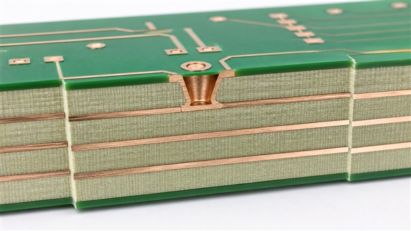
Blind, buried, stacked or filled vias Additional lamination cycles, alignment risk and unclear fill requirements Via span, stacking or staggering, fill type, copper cap, planarization and sequential-lamination plan
Large copper-free areas or uneven plane density Resin-flow imbalance, thickness variation, plating non-uniformity or bow and twist Copper-balancing method, clearance constraints, panel orientation and acceptable bow and twist

Multilayer PCB Case Analysis: From Design Requirements to Production Output

This representative, non-customer-specific multilayer PCB manufacturing case shows how a design can move from technical requirements to a controlled production package. It uses values within the supplied rigid-board capability table and does not claim a named customer, measured yield or field-performance result.

Project background

The example is a 10-layer industrial control board that combines dense digital routing, dedicated power and ground planes, controlled-impedance nets and connectors that must align with an existing enclosure. The prototype is intended to become the reference build for repeat production.

Project requirements

  • Board construction: 10 layers, 1.6 mm finished thickness and a symmetrical high-Tg FR-4 stackup.
  • Circuit geometry: 1 oz inner and outer copper with 4/4 mil minimum line and spacing.
  • Hole structure: 0.20 mm minimum finished plated holes within an 8:1 through-hole aspect ratio.
  • Electrical control: Defined impedance targets, reference planes and coupon requirements.
  • Final verification: ENIG surface finish, electrical test, dimensional inspection and agreed quality records.
Engineering solution

  • Stackup review: Check symmetry, dielectric selection, copper balance and impedance feasibility before routing is frozen.

  • DFM closure: Review annular rings, drill-to-copper clearance, panel utilization and fabrication-note consistency.
  • Prototype control: Use the first build to verify dimensions, hole structure, impedance evidence and assembly fit.
  • Release control: Freeze fabrication, drill, netlist, BOM, placement and test files under one approved revision.

Output result

The defined output is a revision-controlled prototype and production package containing the approved stackup, closed DFM actions, fabrication data, inspection requirements and test records. Actual electrical, assembly and field results must be confirmed from the manufactured project rather than inferred from this representative example.

What Multilayer PCB Services Does EBest Circuit Provide?

EBest Circuit provides coordinated support from design review and prototyping through production, sourcing and assembly. Keeping the release package under one engineering workflow reduces revision mismatches between bare-board and assembly data.

  • PCB design and DFM: Review stackup symmetry, materials, finished copper, via architecture, impedance structures and fabrication notes.
  • Prototype verification: Confirm thickness, hole structure, impedance, assembly fit and inspection evidence before production release.
  • Mass production: Control revisions, materials, repeatability, traceability and inspection requirements across production lots.
  • Component sourcing: Coordinate BOM availability, approved alternatives and component changes with the assembly release.
  • PCB assembly: Review land patterns, surface finish, panel format, placement data, programming method and test plan.

What Are EBest Circuit’s Multilayer PCB Manufacturing Capabilities?

EBest Circuit’s supplied rigid-board capability table separates preferred production limits from special-process limits. Special-process values require an engineering review of the complete stackup, panel design, copper distribution and acceptance criteria.

Capability item Standard process Special process Engineering note
FR-4 layer count 1-10 layers; high-Tg material required from 8 layers 10-32 layers Final feasibility depends on stackup, thickness, via structure and registration margin.
Inner-layer copper 0.5-5 oz 5-20 oz Heavier copper requires wider conductors and spacing plus adequate resin fill.
Outer-layer copper 1-5 oz 5-20 oz Finished copper should be stated clearly because plating affects final geometry.
Minimum finished hole 0.20 mm 0.15 mm Review drill size together with finished thickness and required plating.
Through-hole aspect ratio 8:1 10:1 Lower ratios generally provide a wider plating process margin.
Inner-layer line/space at 1 oz 4/4 mil 3/3 mil Copper weight changes the achievable line and spacing values.
Outer-layer line/space at 1 oz 4/4 mil 3/3 mil Do not apply the 1 oz rule to heavier finished copper without review.
Processed board thickness Typically 0.4-3.5 mm, depending on surface finish; hard-gold-finger combinations start at 1.0 mm Nonstandard thicknesses above 0.15 mm and below 8.0 mm require review Layer count, panel size and surface finish can narrow the usable range.
Available surface finishes OSP, HASL, ENIG, immersion silver, immersion tin, ENEPIG and hard gold fingers Combination finishes subject to review Select the finish around assembly, contact, shelf-life and application requirements.

Capability limits should never be evaluated one row at a time. A design may meet the individual line, hole and layer-count limits yet still require special processing when those limits occur together. Submit the actual fabrication data for DFM confirmation before treating a stated maximum as a production commitment.

Why Choose EBest Circuit for Multilayer PCB Manufacturing?

Choose EBest Circuit when the project needs engineering review, transparent process limits and coordinated support from prototype through assembly. The final sourcing decision should still be based on the actual stackup, via structure, inspection plan and acceptance criteria.

  • Engineering-led DFM: Review stackup, via structure, copper geometry and special-process requirements before production release.
  • Transparent capability limits: Separate standard production windows from values that require additional engineering confirmation.
  • Material and traceability control: Align laminate selection, approved alternatives and required lot records with the purchase specification.
  • Inspection planning: Coordinate AOI, electrical test, microsection, impedance and report requirements around product risk.
  • Integrated project support: Connect design review, prototyping, production, component sourcing and PCB assembly within one release workflow.
  • Revision-matched quotation: Review the same fabrication files, specifications and acceptance criteria used for production.

For available build options and supplier support, review EBest Circuit’s multi-layer PCB fabrication capabilities, then submit the actual production files for confirmation.

What Files Are Needed for a Multilayer PCB Quote?

An accurate multilayer PCB manufacturing quote requires one complete, revision-matched fabrication package. Include Gerber or ODB++ data, NC drill files, a fabrication drawing, stackup information, quantity and any controlled-impedance, testing, material or documentation requirements. Assembly quotations also require a BOM and pick-and-place data.

State the finished board thickness, copper requirements, surface finish, smallest finished hole, special vias, tolerances, panel or delivery format and intended production volume. If the stackup is not final, explain the electrical constraints and ask the supplier to propose a manufacturable construction rather than silently assuming a generic stackup.

Frequently Asked Questions About Multilayer PCB Manufacturing

Q1: Can an odd-layer multilayer PCB be manufactured?

A1: Yes, but an even, symmetrical construction is usually preferred. An odd-layer design may need an additional nonfunctional copper layer or a revised stackup to improve dimensional and thermal balance.

Q2: When should high-Tg laminate be specified?

A2: Consider high-Tg material when the board will face higher assembly temperatures, repeated thermal cycles or demanding service conditions. Tg alone does not define reliability; decomposition temperature, expansion behavior and the full laminate system also matter.

Q3: Should laminate substitutions be allowed on the fabrication drawing?

A3: Allow substitutions only through a defined approval process. The alternative should match the required electrical, thermal, mechanical and compliance properties, especially for controlled-impedance or qualification-sensitive products.

Q4: When is via filling required?

A4: Via filling may be needed for via-in-pad structures, stacked microvias, planar assembly surfaces or specific thermal paths. State the fill type, planarization and copper-cap requirements instead of using the word “filled” without a process definition.

Q5: When should back drilling be considered?

A5: Back drilling is useful when unused plated-through-hole stubs could affect high-speed signal integrity. The drawing should define the target layers, residual stub requirement, drill tolerance and any coupon or inspection expectation.

Q6: Does panelization need to be finalized before the first prototype?

A6: Not always, but early panel discussion helps uncover edge clearance, tooling, breakaway and assembly-handling constraints. The volume-production panel should be reviewed again when board outline, assembly method or production quantity changes.

Q7: Should bare multilayer PCBs be baked before assembly?

A7: Baking is not an automatic requirement for every board. Decide from moisture exposure, storage history, laminate guidance, surface finish and the assembly profile; unnecessary baking can also affect solderability or materials.

Q8: How should engineering changes be controlled after prototype approval?

A8: Release changes through a documented revision process covering fabrication data, drill files, drawings, stackup, BOM, placement data and test files. Mixing revisions is a common and preventable source of production errors.

Q9: Which production records should a buyer request?

A9: Request only records that support the product risk and acceptance plan. Useful options can include electrical-test confirmation, impedance results, microsection evidence, material traceability and inspection reports.

Q10: How should unused internal copper areas be handled?

A10: Coordinate copper thieving or balancing with the fabricator when large empty areas could affect plating uniformity, resin flow or dimensional stability. Any added copper must preserve electrical clearance and the intended plane behavior.

Summary

Multilayer PCB manufacturing succeeds when the stackup, materials, copper geometry, via structure and acceptance criteria are treated as one production system. Inner-layer AOI protects the build before lamination; controlled drilling, desmear and plating create reliable interconnections; final inspection verifies the finished result. Early DFM review reduces avoidable schedule and yield risk.

If you are sourcing multilayer PCB fabrication or PCBA support, contact EBest Circuit at sales@bestpcbs.com. For a faster engineering review and a more accurate quotation, submit Gerber or ODB++, NC drill files, BOM, quantity, approved or proposed stackup, assembly scope, firmware or programming method, test requirements and required quality documentation.

You may also like

Potentiometer Wiring Guide: 3-Pin Diagram, PCB Connection and Common Errors

July 15th, 2026

Potentiometer wiring depends on the job the component must perform. Use all three pins when the potentiometer is a voltage divider: connect the two outer terminals across the reference voltage and ground, then take the adjustable output from the center wiper. Use the wiper and one outer terminal when it is a variable resistor, preferably tying the unused outer terminal to the wiper so an intermittent wiper does not leave the circuit completely open.

Three-pin rotary potentiometer mounted on a PCB with the wiper and end terminals identified

What Do the Three Potentiometer Pins Do?

A standard three-pin potentiometer contains a fixed resistive track between two end terminals and a movable wiper connected to the middle terminal. The resistance measured between the two outer pins remains close to the rated value regardless of shaft position. Resistance from the wiper to either end changes as the shaft turns, while the two wiper-to-end measurements should add to approximately the total track resistance.

  • End terminal 1: one side of the fixed resistive element.
  • Wiper: the adjustable contact that moves along the element.
  • End terminal 2: the other side of the fixed resistive element.

Do not assume the center physical pin is always the wiper on every special package. Confirm the pinout in the manufacturer drawing or with a multimeter before releasing a PCB footprint.

How Does 3 Pin Potentiometer Wiring Work as a Voltage Divider?

In a voltage-divider connection, the two end pins establish the full input range and the wiper provides a variable fraction of that voltage. A common arrangement connects one end to VCC, the other to ground, and the wiper to an analog input. Reversing the two end connections does not damage a passive potentiometer, but it reverses the direction in which the output rises.

With an unloaded linear potentiometer, the ideal wiper voltage is approximately the input voltage multiplied by the fraction of track resistance below the wiper. Real circuits can differ because the receiving input loads the divider. Keep the input impedance comfortably higher than the potentiometer resistance when accurate position sensing matters.

How Do You Wire a Potentiometer as a Variable Resistor?

A variable-resistor, or rheostat, connection uses the wiper and one end terminal to place an adjustable resistance in series with a circuit. Connecting the unused end terminal to the wiper is a common fail-safer arrangement: if the wiper momentarily loses contact, the circuit tends toward the full track resistance instead of an open connection. This does not make the part suitable for power control beyond its rating.

Comparison of potentiometer voltage-divider wiring and variable-resistor wiring on PCB modules

Check both the total power rating and the wiper current. A small panel or trimmer potentiometer should not be used to control a motor, heater, lamp, or other high-current load directly; use it as a control signal for an appropriate driver circuit.

Potentiometer Wiring Diagram for Common Applications

The correct potentiometer wiring diagram is determined by the circuit function, not by wire color. The table below shows practical starting points that should still be verified against the schematic and component datasheet.

Application End Pin 1 Wiper End Pin 2 Design Note
Analog voltage input VCC or reference ADC input Ground Add filtering and input protection when the cable or environment is noisy.
Audio volume control Signal input Amplifier input Signal ground Use the specified audio/log taper and control grounding carefully.
Adjustable resistance Series input Series output Tie to wiper or leave only if the design requires it Check wiper current and power over the full adjustment range.
Calibration trimmer Reference node Feedback or trim node Second reference node Confirm the safe startup state and adjustment direction.

How Should a Potentiometer PCB Connection Be Designed?

A reliable potentiometer PCB connection begins with the exact mechanical drawing. Match pin pitch, hole size, shaft position, body clearance, mounting tabs, panel height, and rotation envelope. Mechanical tabs may carry load but are not automatically electrical terminals. Keep silkscreen pin labels visible after assembly and mark the rotation direction or minimum/maximum function when technicians need it.

Route the wiper as a sensitive analog node when it feeds an ADC, amplifier, or feedback circuit. Keep it away from switch nodes, high-current loops, clocks, relays, and motor traces. A short trace, a nearby RC filter, a defined ground return, and ESD protection at user-accessible controls can reduce noisy readings. For panel-mounted controls connected by cable, define the connector pinout and cable shield strategy before layout.

Potentiometer PCB layout showing a short wiper trace, RC filter near the MCU ADC, and separation from a switching node

Linear vs Logarithmic Potentiometer Wiring

Linear and logarithmic potentiometers can use the same three electrical connections, but their response to shaft position is different. A linear taper changes resistance approximately in proportion to rotation and is common for sensing, calibration, and control voltages. A logarithmic or audio taper changes more gradually at one end and better matches human loudness perception.

Replacing an audio taper with a linear part may produce a volume control that feels abrupt even though the wiring is correct. Replacing a linear sensor potentiometer with an audio taper can distort the relationship between position and measured voltage. Include resistance value, taper, rotational life, tolerance, power rating, shaft style, and mounting details in the BOM rather than specifying only the resistance.

Common Potentiometer Wiring Errors and Their Symptoms

Most potentiometer faults come from a wrong pin assumption, a reversed end connection, a floating wiper, or mechanical stress at the PCB joint. Diagnose the symptom systematically instead of swapping wires at random.

Symptom Likely Cause Check Correction
Output moves in the wrong direction Outer terminals reversed Compare shaft direction with wiper voltage Swap the two end-terminal connections.
Output is fixed at one rail Wiper misidentified, shorted, or open Measure wiper-to-end resistance while turning Correct pin mapping and inspect solder joints.
Reading jumps or crackles Dirty track, worn wiper, vibration, or noisy routing Monitor resistance and voltage slowly across travel Replace the part or improve filtering and layout.
Component overheats Excess track power or wiper current Calculate worst-case dissipation at every position Use a suitable driver or higher-rated component.
PCB pads crack Panel force transferred into soldered pins Inspect joints and mechanical support Add bracket, mounting hardware, or strain relief.

How Do You Test Potentiometer Wiring With a Multimeter?

Testing is fastest when the potentiometer is isolated from parallel circuit paths. With power removed, measure the two outer terminals first; the reading should be close to the rated resistance. Then measure from the wiper to each outer terminal while rotating the shaft slowly. One reading should increase while the other decreases, and abrupt opens or unstable jumps indicate a worn track, poor contact, or bad solder joint.

Unpowered three-pin potentiometer being tested for end-to-end resistance and wiper resistance with a digital multimeter
  1. Disconnect power and discharge the circuit.
  2. Identify the pair with nearly constant total resistance.
  3. Identify the wiper by its changing resistance to both ends.
  4. Check for smooth change across the usable rotation.
  5. Power the circuit and verify wiper voltage only after confirming the pinout.

What Should Be Checked Before PCB Assembly?

Before assembly, compare the schematic symbol, footprint numbering, BOM, datasheet view, and physical sample as one chain. Component drawings may show a bottom view while the PCB layout is viewed from the top, which can mirror the pin order. Confirm plated-hole diameter, annular ring, body keepout, mounting hardware, wash compatibility, soldering temperature, and whether the shaft or adjustment screw remains accessible in the enclosure.

During inspection, verify component orientation, solder wetting, mechanical seating, and the expected end-to-end resistance. A qualified PCB assembly services workflow should also include a functional test that records the minimum, midpoint, and maximum output rather than checking only continuity.

FAQs About Potentiometer Wiring

Which pin is the wiper on a potentiometer?

The wiper is commonly the middle pin on a standard three-terminal rotary potentiometer, but special packages can differ. Verify it with the datasheet or by measuring resistance: the wiper shows a changing resistance to both end terminals as the shaft turns.

Can I swap the two outer potentiometer pins?

Yes, swapping the two outer pins usually reverses the direction of adjustment. In a voltage divider, clockwise rotation may then decrease rather than increase the wiper voltage. Confirm that the resulting direction matches the user interface and safety requirements.

What happens if the wiper is not connected?

If only the two outer pins are connected, the component acts as a fixed resistor equal to its full track resistance. Rotating the shaft will not change that end-to-end value. A circuit expecting an adjustable output will therefore not respond.

Why tie the unused terminal to the wiper?

When a potentiometer is used as a variable resistor, tying the unused end terminal to the wiper provides a second electrical path at the wiper node. If contact becomes intermittent, the resistance tends toward the full track value instead of becoming completely open.

Does potentiometer wiring depend on resistance value?

The basic connection does not, but resistance value affects loading, current, noise, and power. A value that is too low wastes current and can exceed power limits; a value that is too high may be sensitive to leakage, interference, or ADC input behavior.

Can a potentiometer control a motor directly?

A small signal potentiometer should not carry motor current directly. Use it to produce a control voltage for a motor driver, PWM controller, or suitable transistor stage. Verify the potentiometer’s track power and wiper-current ratings.

Why does a potentiometer produce a noisy ADC reading?

Noise can come from a worn wiper, long wiring, poor grounding, nearby switching nodes, or insufficient settling time. Shorten the wiper route, add an appropriate RC filter, improve the reference and ground path, and confirm the ADC source-impedance requirement.

What is the difference between a potentiometer and a rheostat?

A potentiometer normally uses three terminals as a voltage divider. A rheostat function uses two effective terminals to provide variable resistance. The same three-terminal component can sometimes perform either role, but its current and power ratings still apply.

How do I identify potentiometer pin 1?

Use the manufacturer drawing and note whether it is a top, bottom, or shaft-side view. Pin 1 may be marked by numbering, a molded feature, or the PCB silkscreen. Do not assign pin 1 solely from left-to-right appearance.

Should the potentiometer body be connected to ground?

Only when the datasheet or system grounding plan calls for it. A metal case or mounting tab may be a shield, a mechanical feature, or electrically isolated. Measure and verify its purpose before connecting it to signal or chassis ground.

Build a Reliable Potentiometer Interface

Reliable potentiometer wiring comes from confirming the wiper, selecting the correct divider or variable-resistor connection, protecting the analog node, and designing the footprint around the real mechanical part. If you are developing a control PCB, review the available PCB and PCBA manufacturing capabilities, then provide the schematic, Gerber files, BOM, potentiometer datasheet, enclosure constraints, and functional test limits so the assembly team can assess both electrical and mechanical risks.

If you’re sourcing reliable PCB/PCBA manufacturing, including OEM, ODM, prototyping, mass production, or custom engineering solutions, reach out to our engineering team for technical support and a quote at sales@bestpcbs.com.


You may also like

Inductor Symbol: Meaning, Types, Standards, and Circuit Diagram Examples

July 14th, 2026

The inductor symbol is normally drawn as a coil or a row of curved loops. Extra lines, arrows, taps, or dots may identify an adjustable winding, magnetic core, intermediate connection, or magnetic coupling.

Recognizing the mark is only the first step. A schematic symbol identifies electrical function, but it does not contain enough information to purchase or assemble the physical part. Engineers must also confirm inductance, tolerance, current ratings, DC resistance, frequency behavior, package, footprint, and operating temperature.

Inductor symbol beside an L1 component mounted on a PCB

What Is an Inductor Symbol and What Does It Mean?

An inductor symbol represents a passive component that stores energy in a magnetic field while current flows through it. The familiar coil shape comes from the traditional construction of conductive wire wound around air or a magnetic core.

A basic inductor has one winding and two terminals. Its ideal voltage-current relationship is:

v = L × di/dt

The voltage across the part is proportional to the inductance and the rate at which current changes. This is why an ideal inductor resists sudden changes in current. Its stored magnetic energy is:

W = ½LI²

In practical circuits, inductors provide energy storage, ripple-current control, filtering, impedance matching, and EMI suppression. The symbol does not reveal whether the physical part is wire-wound, multilayer, molded, shielded, toroidal, or intended for RF use. Those details come from the BOM and datasheet.

Why Is Inductance Represented by L, and What Is Its Unit?

Inductance is represented by L. The letter is commonly associated with Lenz’s law, although historical explanations vary. The SI unit is the henry, written as H.

Marking Meaning Example
L Inductance as a physical quantity L = 10 µH
L1, L2 Reference designators L1 identifies one BOM item
H Henry, the SI unit 1 H
mH Millihenry 10 mH
µH Microhenry 4.7 µH
nH Nanohenry 22 nH

For example, “L1 4.7 µH” combines a reference designator with a nominal value. L1 links the part to the BOM and PCB layout, while 4.7 µH states its inductance.

An inductor’s ideal AC reactance is XL = 2πfL. Reactance rises with frequency, but a real part also has winding resistance and parasitic capacitance. Above its self-resonant frequency, it may no longer behave mainly as an inductor. RF selection therefore requires the SRF and Q factor, not only the nominal value.

What Are the Main Types of Inductor Symbols?

Inductor symbols are modified to show circuit function rather than package appearance.

Fixed variable magnetic core tapped coupled and common-mode inductor symbols

Type Common symbol feature What it communicates
Fixed inductor Single coil A fixed nominal inductance
Variable inductor Coil with a diagonal arrow The inductance can be adjusted
Magnetic-core inductor Parallel lines beside the coil A magnetic core is present
Tapped inductor Connection from the winding An intermediate terminal is available
Coupled inductor Two or more adjacent coils The windings are magnetically coupled
Common-mode choke Coupled windings in separate conductors Common-mode noise filtering

A shielded, molded, toroidal, or multilayer inductor may still use the generic fixed-inductor symbol. The exact physical construction is normally defined by the selected manufacturer part number.

How Do Fixed, Variable, Air-Core, Iron-Core, and Ferrite-Core Inductor Symbols Differ?

The clearest graphical distinction is between fixed and adjustable inductors. Core-material differences are less consistent because ECAD libraries do not always use identical qualifying marks.

Type Typical symbol cue Engineering behavior Common use
Fixed Plain coil Fixed nominal value Power conversion, filtering and RF
Variable Diagonal arrow Adjustable for tuning or calibration RF matching and resonant circuits
Air-core Usually no core lines No magnetic-core saturation; lower inductance per volume High-frequency and RF circuits
Iron or powder core Magnetic-core qualifier Useful energy storage; powder cores often saturate gradually Power filters and converters
Ferrite core Magnetic-core qualifier High permeability; saturation can be more abrupt Switching supplies, transformers and EMI filters

The drawing alone may not distinguish ferrite, powdered iron, metal composite, or a gapped core. For power-inductor selection, compare nominal inductance, saturation current, RMS current, DCR, core loss, package height, shielding, and operating temperature.

Selection rule: Isat is linked to inductance loss under DC bias, while Irms is linked to temperature rise from winding loss. Both ratings must cover the real operating condition with suitable margin.

What Do Core Lines and Dots Mean on an Inductor Symbol?

Magnetic core lines and winding polarity dots on inductor symbols

Parallel lines beside or between windings normally indicate a magnetic core. They do not identify the exact material, air gap, saturation current, core loss, or shielding performance. Those parameters remain part-specific.

Dots serve a different purpose. On coupled windings, they mark corresponding instantaneous polarity, often called winding phase. When current enters the dotted terminal of one winding, the induced voltage in the other winding is positive at its dotted terminal under the same reference convention.

The dot convention matters in coupled inductors, transformers, flyback converters, SEPIC converters, and common-mode chokes. It is not a positive or negative marking for an ordinary two-terminal inductor.

How Do IEC and ANSI/IEEE Inductor Symbols Differ?

IEC and legacy ANSI/IEEE documentation can use different coil geometry and qualifying marks, yet both describe the same electrical function. Modern drawings also vary between Altium Designer, KiCad, OrCAD, EAGLE, LTspice, and internal company libraries.

IEC 60617 and legacy ANSI IEEE symbol standards with library consistency guidance

IEC 60617 is the current IEC graphical-symbol database for electrotechnical diagrams. ANSI/IEEE 315 and its supplements remain familiar references in older North American documentation, but they are listed by IEEE as inactive-reserved.

For a new design, consistency is more valuable than selecting a symbol only for regional appearance. A controlled library should define symbol geometry, reference-designator rules, pin numbering, dot placement, value formatting, and approved footprints. When reviewing legacy drawings, use the legend, BOM, and surrounding circuit to confirm meaning.

How Do You Read an Inductor Symbol in a Circuit Diagram?

Use the symbol as an entry point, then confirm the component through the design data.

Checklist for reading an inductor symbol and verifying its PCBA specification

  1. Find the reference designator. L1 or L205 links the symbol to the BOM, assembly drawing, PCB layout, and test records.
  2. Read the inductance value. Confirm whether the value is in nH, µH, or mH and avoid ambiguous decimal notation.
  3. Check qualifying marks. An arrow indicates adjustment; parallel lines suggest a core; a tap adds a winding terminal; multiple coils and dots indicate coupling.
  4. Inspect the surrounding circuit. An inductor beside a switching regulator is probably an energy-storage part. One near an antenna may belong to an RF matching network.
  5. Match the BOM and datasheet. The schematic value alone is not a purchase specification.
  6. Verify the footprint. Confirm pad geometry, pin numbering, courtyard, component height, and assembly orientation.

A useful BOM entry includes the manufacturer part number, inductance, tolerance, package, Isat, Irms, maximum DCR, operating temperature, and approved alternates. RF parts may also require Q and SRF. EMI chokes may require impedance-versus-frequency data and isolation ratings.

For a turnkey PCBA quotation, EBest Circuit (Best Technology) can review the schematic for circuit context, but the production package should still include Gerber or ODB++, BOM, centroid data, assembly drawings, and exact component information. This prevents delays caused by incomplete descriptions or symbol-to-footprint mismatches.

How Is an Inductor Symbol Used in Common Circuits?

Inductor symbols in a buck converter and common-mode filter with passive component comparison

Buck Converter

In a buck converter, the inductor sits between the switching node and output capacitor. It stores energy and limits ripple current. Selection should account for input and output voltage, switching frequency, peak current, ripple target, DCR, saturation current, and temperature rise.

Too little inductance raises ripple and peak current. Excessive inductance can increase package size, DCR, cost, and transient-response time. The part must remain within its thermal and saturation limits during startup, overload, and current limiting.

Boost Converter

In a boost converter, the inductor is commonly connected between the input supply and switching node. Peak inductor current can be much higher than output current, especially at low input voltage. Using load current alone as the selection basis can therefore produce an undersized part.

LC Filter

An inductor and capacitor can form a power or signal filter. Their values must be evaluated with source impedance, load impedance, ESR, DCR, tolerance, and damping. An undamped LC network may create ringing even when its nominal cutoff frequency appears correct.

RF Matching Network

RF inductors are used with capacitors for matching and resonance. At high frequency, Q, SRF, package parasitics, PCB pads, trace inductance, and ground-via placement can materially change the result. Two parts with the same nominal value may behave differently because of package and construction.

EMI and Common-Mode Filtering

A single inductor can attenuate differential-mode noise. A common-mode choke uses coupled windings to impede noise traveling in the same direction on multiple conductors. Evaluate the impedance curve at the actual interference frequency rather than relying only on a low-frequency inductance value.

Inductor vs Capacitor vs Resistor vs Transformer Symbols

The fastest identification method is to compare symbol shape, reference letter, and winding count.

Component Typical appearance Reference letter Main function
Inductor One coil L Stores magnetic energy and resists current change
Capacitor Two plates C Stores electric-field energy and resists voltage change
Resistor Zigzag line or rectangle R Limits current or creates a voltage drop
Transformer Two or more coupled coils T or TR Transfers energy or signals by magnetic coupling

A single inductor normally has one winding and two terminals. A transformer has at least two windings and may provide isolation or a turns ratio. A coupled inductor can resemble a transformer, so the topology, winding data, isolation rating, and datasheet must also be checked.

FAQs About Inductor Symbols

1. What is the standard symbol for an inductor?

The generic symbol is a coil or series of curved loops between two terminals. Exact geometry varies between IEC, legacy ANSI/IEEE, and ECAD libraries.

2. Why is an inductor represented by the letter L?

Inductance is conventionally represented by L, often associated with Lenz’s law. The historical origin is not completely certain. Labels such as L1 and L2 identify individual components in a design.

3. What does L1 mean on a circuit diagram?

L1 is a reference designator. It connects the schematic symbol to the corresponding BOM entry, footprint, assembly location, and test record. It does not state the inductance value.

4. What is the unit symbol for inductance?

The SI unit is the henry, written as H. PCB-mounted inductors are commonly specified in mH, µH, or nH.

5. Do inductors have polarity?

Most basic two-terminal inductors do not have positive and negative terminals. Orientation can still matter for coupled, tapped, or magnetically sensitive parts and for devices with start-of-winding marks.

6. What do the lines and dots beside an inductor symbol mean?

Parallel lines normally indicate a magnetic core. Dots on coupled windings show relative winding phase. Neither mark provides a complete material or current specification.

7. What is the difference between an inductor symbol and a transformer symbol?

An inductor normally shows one winding. A transformer shows two or more magnetically coupled windings. Coupled inductors can look similar, so confirm the part from the circuit and datasheet.

Conclusion

The inductor symbol identifies an inductive function, but it does not fully define the component. Core construction, current capability, DCR, frequency behavior, package, footprint, and thermal limits must be confirmed before layout, purchasing, or assembly.

For a PCBA quotation, provide Gerber or ODB++ data, BOM, centroid files, assembly drawings, and complete inductor specifications. EBest Circuit supports PCB manufacturing, component sourcing, prototype assembly, and turnkey production. Contact sales@bestpcbs.com for project review or quotation.

You may also like

Custom Number Pad PCB: Design, Matrix Layout and Manufacturing

July 14th, 2026

A custom number pad PCB is a purpose-built circuit board that connects a numeric key layout, switch matrix, controller and wired or wireless interface in one production-ready assembly. A reliable design starts with the user interface and enclosure, then translates that geometry into switch footprints, row-and-column scanning, diode orientation, connector protection, fabrication data and a repeatable test plan.

That sequence matters. A numpad can work on a development bench and still fail in production because a hot-swap socket collides with the enclosure, a diode direction does not match the firmware, a USB-C connector lacks the required configuration resistors, or the assembly supplier receives incomplete files. This guide shows engineers, buyers and product teams how to move from a custom layout to a PCB and PCBA package that a manufacturer can quote, build and inspect without guessing.

Custom Number Pad PCB

What Is a Custom Number Pad PCB?

A custom number pad PCB is the electrical and mechanical platform for a numeric keypad made for a specific product, layout or workflow. Unlike a replacement PCB for an existing retail numpad, a custom board can change the key count, key positions, macro functions, switch technology, interface, mounting pattern, controller and enclosure.

The term can describe several products:

  • A mechanical numpad with MX-style or low-profile switches.
  • A programmable macropad that includes numbers, shortcuts, a rotary encoder or display.
  • An industrial data-entry panel with tactile switches, metal domes or a membrane interface.
  • A compact control PCB integrated into a larger instrument, terminal or machine.
  • A wired USB device or a battery-powered wireless input module.

The PCB is only one part of the input system. It must fit the plate and enclosure, accept the selected switches, scan every key reliably, communicate with the host and survive assembly and use. For a broader overview of full-size and compact keyboard projects, see the Best Technology guide to custom keyboard PCB development.

Which Numpad Architecture Fits the Product?

The right architecture depends on whether the number pad is a finished USB device, a keypad module inside another product or a low-power wireless controller. Decide this before assigning controller pins or routing the board.

Architecture Best fit Key design decisions Production concern
USB numpad Desktop data entry, POS accessories, programmable controls USB-capable MCU, Type-C or legacy connector, ESD and firmware Connector strength, USB compliance and functional testing
Matrix keypad module Industrial equipment, instruments and embedded products Row/column connector, voltage levels, cable length and host scanning Connector pinout, noise immunity and system-level test access
Wireless numpad Portable or cable-free products Radio module, antenna clearance, battery management and sleep current RF layout, enclosure material, certification scope and power test
Industrial front-panel keypad Sealed controls and repetitive data entry Metal dome, membrane or tactile switch interface; ESD and ingress strategy Overlay stack-up, actuation consistency and environmental validation

A stand-alone USB numpad usually needs the most integration on the PCB. A passive matrix keypad may need no onboard MCU, but the row/column interface, cable pinout and host-side scanning must be defined. Wireless designs add antenna, power and regulatory constraints that should not be treated as a simple variation of the wired board.

How Should the Key Matrix and Diodes Be Designed?

A numpad matrix arranges switches at row-and-column intersections so the controller can scan many keys with fewer I/O pins. A 5-by-4 matrix, for example, can address up to 20 switch positions with nine matrix signals, although the actual layout may leave some intersections unused.

During scanning, firmware drives or reads one side of the matrix and checks the other side to identify a closed switch. The official QMK matrix explanation illustrates why multiple simultaneous keypresses can create unintended current paths. A diode in series with each switch makes current directional and helps prevent ghost keys.

How Should the Key Matrix and Diodes Be Designed?

Use this matrix checklist before layout:

  1. List every key, encoder push switch and auxiliary button in a matrix table.
  2. Choose row and column counts that fit the available MCU pins and expected expansion.
  3. Assign one reference designator to every switch and diode.
  4. Use a single diode orientation across the board unless the design has a documented exception.
  5. Set the firmware diode direction to match the schematic. QMK exposes this through its matrix configuration options.
  6. Reserve accessible test points for rows, columns, power, ground and reset.
  7. Review simultaneous-key requirements instead of testing only one key at a time.

A small numpad may appear to work without per-key diodes when users press one key at a time. That does not prove the matrix is safe from ghosting. Diodes are especially important when the product supports shortcuts, macros, gaming inputs or any action that combines multiple keys.

How Do You Choose Switches, Hot-Swap Sockets and Key Spacing?

Choose the input technology before creating footprints because the switch, socket, plate and enclosure form one mechanical stack. A footprint that is electrically correct can still be unusable if the switch orientation, stabilizer cutout or component height is wrong.

Input option Advantages Trade-offs Layout checks
Soldered mechanical switch Simple BOM and strong retention Switch replacement requires soldering Pin pattern, center post, plate cutout and stabilizers
Hot-swap socket Replaceable switches and easier product customization More underside area and tighter enclosure constraints Socket orientation, copper clearance, solder access and bottom-case height
Low-profile switch Thinner product Different footprint, plate and keycap ecosystem Exact manufacturer drawing and total stack height
Tactile switch or metal dome Compact industrial interface Different feel and front-panel construction Contact geometry, actuation force, overlay and venting strategy

Many mechanical layouts use a 19.05 mm key pitch, but that value is not a universal rule. Start from the chosen switch and keycap drawings, then define the plate, PCB and enclosure from one controlled coordinate system. Pay special attention to double-width Enter or Plus keys, stabilizer locations, rotary encoders, displays and USB connector openings.

What Should a USB-C Numpad Circuit Include?

A USB-C numpad circuit needs more than the connector footprint: it must define device orientation detection, power protection, data routing and mechanical retention. For a basic USB 2.0 device using a Type-C receptacle, both CC pins normally require their own pull-down resistor to identify the board as a sink/device. Confirm the resistor value and implementation against the current USB Type-C specification and the selected connector or controller documentation.

The schematic and layout review should cover:

  • CC1 and CC2 configuration for a device-only port.
  • VBUS protection appropriate to the product risk and power path.
  • ESD protection placed close to the connector.
  • D+ and D− routing as a short, coupled pair with a continuous return path.
  • Decoupling capacitors located close to MCU power pins.
  • Connector shell grounding and mounting tabs based on the connector datasheet.
  • Accessible reset and programming pads.
  • Cable insertion clearance and enclosure wall thickness.

Do not copy a Type-C connector symbol or footprint without checking its pin mapping and mechanical drawing. A footprint mismatch can produce a board that looks correct in CAD but cannot be assembled or connected reliably. The BestPCBs article on USB port pin configuration provides additional connector context.

How Should the PCB Match the Plate and Enclosure?

The PCB, switch plate and enclosure should be designed from a shared mechanical datum and verified together in 3D. Board outline, mounting holes, connector openings and key centers must use controlled dimensions rather than visual alignment.

Review the following interfaces:

  • Key centers: Export coordinates from the approved layout and lock them before detailed routing.
  • Mounting holes: Define finished hole size, keepout, fastener head diameter and any plated or non-plated requirement.
  • Board edge: Maintain clearance between copper/components and routed edges based on the fabricator’s rules.
  • Connector position: Check insertion path, cable overmold and strain on the solder joints.
  • Hot-swap sockets: Verify bottom-case clearance and prevent ribs or batteries from touching sockets.
  • Component height: Place the tallest parts in permitted zones and include tolerance, not only nominal dimensions.
  • ESD path: Consider where a user can touch exposed metal, a rotary encoder shaft or connector shell.

A STEP model or enclosure assembly review is useful, but it does not replace a dimensioned drawing. Include critical dimensions and tolerances in the controlled design package so the PCB, plate and enclosure suppliers work from the same revision.

What Files Are Required for Fabrication and Assembly?

A reliable quotation and build require a complete, revision-controlled fabrication and assembly package. Gerbers alone may be enough for a bare board quote, but they are not enough for turnkey PCBA.

File or document Purpose Numpad-specific checks
Gerber or ODB++ fabrication data Defines copper, solder mask, silkscreen, paste and board outline Switch pads, socket paste openings, USB tabs and outline are on correct layers
Excellon drill files Defines plated and non-plated holes Switch posts, stabilizers and mounting holes are classified correctly
Fabrication drawing/readme States stack-up, thickness, finish, impedance if required and special notes Board thickness matches switches, sockets, plate and enclosure
BOM Lists manufacturer part numbers, quantities and approved alternates Connector, MCU, diode, ESD device and socket variants are unambiguous
Pick-and-place/centroid file Defines component coordinates, side and rotation Diode polarity and hot-swap socket rotation are verified against the drawing
Assembly drawing Shows reference designators, polarity, do-not-fit parts and notes Key-layout options and variant components are clearly separated
Test specification Defines electrical and functional acceptance Every key, multi-key condition, USB interface, LEDs, encoder and current mode is covered
Firmware/programming package Defines image, method, version and verification Keymap, diode direction, bootloader and product identifier match the PCB revision

KiCad’s official documentation describes the generation of Gerber and drill outputs. Before release, open the exported manufacturing data in an independent viewer. Do not rely only on the native CAD display. BestPCBs also provides practical PCB design tools for trace-width and via-current checks during engineering review.

For a broader supplier-ready package, use the custom PCB assembly services checklist to review BOM, placement data, sourcing and test requirements.

Which DFM Checks Prevent Prototype Re-Spins?

The most valuable DFM review finds electrical, assembly and mechanical errors before the first panel is released. For a custom numpad PCB, the review should go beyond trace width and spacing.

  • Confirm switch, socket, stabilizer, connector and encoder footprints against current datasheets.
  • Run schematic-to-layout checks and verify every row, column and diode reference.
  • Check diode and LED polarity in the schematic, silkscreen, BOM and placement file.
  • Inspect solder mask and paste apertures for hot-swap sockets and connector mounting tabs.
  • Check component-to-edge, copper-to-edge and tool clearance around routed features.
  • Separate non-plated mechanical holes from plated electrical holes.
  • Review USB D+/D− routing, return path, ESD placement and connector shell strategy.
  • Verify annular rings, thermal reliefs and solderability for hand-soldered or through-hole parts.
  • Add readable revision marking and polarity/orientation identifiers.
  • Check panelization, breakaway features and component clearance near panel rails.
  • Compare the final PCB model with the plate and enclosure assembly.
  • Review test-point access after the board is installed in its fixture or enclosure.

Variant control is another common failure point. If one PCB supports several key layouts or optional displays, document fitted and non-fitted parts by assembly variant. Do not leave the assembler to infer the product version from the order name.

How Is a Custom Number Pad PCB Manufactured and Assembled?

Production moves from engineering review to bare-board fabrication, component assembly, inspection and product-specific functional testing. The exact flow depends on the stack-up, component mix, quantity and acceptance plan.

  1. Engineering review: The supplier checks file completeness, fabrication constraints, BOM availability and assembly risks.
  2. Panel and tooling preparation: The board is arranged for fabrication and, when required, automated assembly.
  3. Bare PCB fabrication: Imaging, etching, drilling, plating, solder mask, surface finish, profiling and electrical test create the finished board.
  4. Component preparation: Parts are sourced, verified and assigned to the correct BOM revision and alternates list.
  5. SMT assembly: Solder paste printing, placement and reflow attach the MCU, diodes, ESD devices, LEDs and other surface-mount parts.
  6. Through-hole/manual assembly: Connectors, switches or special components are installed when they are not part of the SMT process.
  7. Inspection: Visual inspection and AOI can verify placement and solder joints; X-ray may be appropriate for hidden-joint packages.
  8. Programming and functional test: When included in the agreed scope, the board is programmed and tested against the approved procedure.
  9. Final inspection and packing: The supplier confirms labeling, quantity, protection and shipment requirements.
Custom number pad PCB assembly undergoing automated optical inspection and functional key testing

Best Technology supports PCB design, prototyping, component sourcing, PCB assembly and small-volume production. Available inspection and test methods documented in the company’s source materials include AOI, X-ray inspection, flying-probe/electrical testing and functional testing. The correct combination should be defined for the actual board rather than copied from a generic quality plan. Learn more about the company’s PCB manufacturing process and PCB assembly capabilities.

How Should the Finished Numpad PCB Be Tested?

A finished numpad needs both board-level checks and a functional test that exercises every input and interface. A bare-board electrical test cannot verify firmware, switch behavior, LEDs, USB enumeration or enclosure interactions.

A practical acceptance plan may include:

  • Power-rail resistance and controlled first power-up.
  • Current consumption in active, idle and sleep modes when applicable.
  • USB enumeration and communication using the approved cable and host conditions.
  • Continuity or scan verification for every row and column.
  • Single-key test for every switch position.
  • Multi-key combinations that could expose ghosting or firmware mapping errors.
  • Rotary encoder direction, push switch, display and indicator LED tests.
  • Reset, bootloader and programming-pad access.
  • Mechanical fit with the production plate, keycaps, enclosure and cable.
  • Stress, ESD, life-cycle or environmental testing defined by the product’s risk and market.

A test fixture can speed up repeatable production checks, but the fixture requirement should be defined early. Add test pads before routing is complete and provide the supplier with the test sequence, pass/fail limits, firmware revision and expected output.

What Drives Prototype and Production Cost?

Cost is driven by board complexity, component choices, assembly operations, testing and order quantity—not by key count alone. A physically small numpad can still be expensive if it uses a high-cost controller, several assembly variants or a complex test fixture.

Cost driver Why it matters Cost-control action
Board size and layer count Affects material use, panel utilization and process complexity Route compactly without compromising switch geometry or test access
Surface finish and specifications Special finishes and tight requirements add process cost Specify what the application needs; avoid unsupported blanket requirements
MCU and connector selection Availability, package and sourcing risk affect price and schedule Use complete MPNs and approve alternates through engineering review
Hot-swap sockets, LEDs and displays Add components, placements and inspection points Offer features only when the product requirement supports their value
SMT and through-hole mix May require multiple assembly operations Design for the intended assembly process from the first prototype
Programming and functional test Requires files, labor, fixtures and failure handling Create a short, deterministic test with clear pass/fail criteria
Variants and quantity Frequent changeovers reduce production efficiency Standardize the base PCB and control variants through BOM and firmware

For a useful comparison, request quotes against the same revision, BOM assumptions, test scope and packing requirements. A lower line-item assembly price may not be lower total cost if it excludes component verification, programming, fixtures or rework responsibility.

How Do You Select a PCB/PCBA Supplier?

Select a supplier by its ability to review the complete product package and control revisions, sourcing, assembly and testing—not only by the bare-board price. The RFQ should make technical scope comparable across suppliers.

Ask these questions:

  1. Will the supplier review the native design or exported fabrication package for DFM and DFA risks?
  2. Can it build both the prototype and the intended production quantity without changing the approved process unexpectedly?
  3. How are BOM substitutions proposed, approved and recorded?
  4. Which inspection methods apply to the actual component package and defect risks?
  5. Can the supplier follow a customer-provided programming and functional test procedure?
  6. How are PCB, BOM, firmware and test revisions linked to the manufacturing order?
  7. Who owns fixtures, programming adapters and product-specific test assets?
  8. What information is required before the quotation becomes firm?
  9. How are nonconformities documented, contained and corrected?
  10. Can the supplier provide one point of coordination for PCB fabrication, component sourcing and assembly if that is required?

Send the same controlled file package to every candidate. If one supplier identifies a real footprint, sourcing or test problem, treat that engineering feedback as part of the comparison rather than focusing only on unit price.

Frequently Asked Questions

What is a custom number pad PCB?

A custom number pad PCB is a circuit board designed for a specific numeric keypad layout, switch type, controller, interface and enclosure. It may operate as a complete USB or wireless device or as a keypad module inside another product.

How does a numpad key matrix work?

A numpad matrix connects switches at row-and-column intersections. The controller scans the rows and columns to identify which intersection has closed, reducing the number of I/O pins required.

Does every numpad switch need a diode?

Use one diode per key when the design must prevent ghosting during multiple simultaneous keypresses. Keep diode orientation consistent and match the firmware’s row-to-column or column-to-row setting.

Can a custom numpad PCB use USB-C?

Yes. A USB-C numpad can use USB 2.0 data, but the schematic must correctly implement CC pins, power protection, ESD control, D+/D− routing and connector mechanics.

What files are needed to manufacture a numpad PCB?

For a bare PCB, provide Gerber or ODB++ data, drill files and fabrication notes. For PCBA, also provide a BOM, pick-and-place file, assembly drawing, approved alternates, firmware package and test specification as applicable.

Should a numpad use hot-swap sockets or soldered switches?

Hot-swap sockets support switch replacement and customization but consume underside space and require careful footprint orientation. Soldered switches simplify the BOM and provide strong retention but are harder to replace.

Can QMK be used for a custom number pad?

Yes, when the selected microcontroller and board configuration are supported. The matrix dimensions, pin assignments, diode direction, keymap and optional features must match the hardware.

How do you prevent ghosting in a keypad matrix?

Place a correctly oriented diode in series with each key, configure firmware to the same direction and test realistic multi-key combinations. A single-key test cannot prove that ghosting is controlled.

What should be tested before mass production?

Test power, USB or host communication, every key, multi-key combinations, LEDs, encoders, reset/programming access and mechanical fit. Add product-specific ESD, life-cycle or environmental tests according to risk.

What affects custom numpad PCB cost?

Key cost drivers include board size and layers, controller and connector choice, switch/socket type, LEDs or displays, SMT and through-hole operations, programming, functional testing, variants and quantity.

How do you choose a numpad PCB manufacturer?

Compare DFM support, revision control, sourcing process, assembly capability, inspection, functional testing and prototype-to-production continuity. Quote every supplier with the same controlled files and acceptance scope.

Can a supplier assemble the PCB and program the controller?

Some PCBA suppliers can do both, but programming is not automatic. Define the firmware image, programming method, security requirements, version verification, fixture ownership and functional test before ordering.

From Prototype to Production

The fastest path to a dependable custom number pad PCB is a controlled release package: approved layout, verified matrix, checked USB interface, complete manufacturing data and a test procedure tied to the same revision. That package gives engineering, procurement and the PCB/PCBA supplier one source of truth.

Best Technology can support PCB design, PCB prototyping, component sourcing and PCB assembly for custom input-device projects. To request an engineering review or quotation, contact Best Technology and include the board files, BOM, target quantity, enclosure constraints and test expectations. The team can then identify missing information and confirm a project-specific manufacturing scope without relying on assumptions.

You may also like