An impedance control PCB can fail even when its Gerber files look correct. A changed dielectric thickness, an unclear reference plane, or an unapproved trace-width adjustment can move the finished impedance outside the required range. The result may be reflections, timing errors, excessive noise, or an interface that works in a prototype but fails after production changes.
The safest approach is to define the electrical target and manufacturing evidence before fabrication begins. This guide explains what customers should release, what a PCB manufacturer should confirm, and how stackup review, test coupons, and time-domain reflectometry (TDR) reports reduce avoidable production risk.
What Is an Impedance Control PCB?
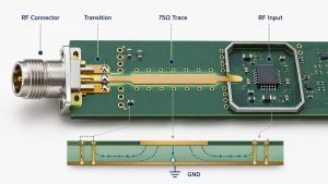
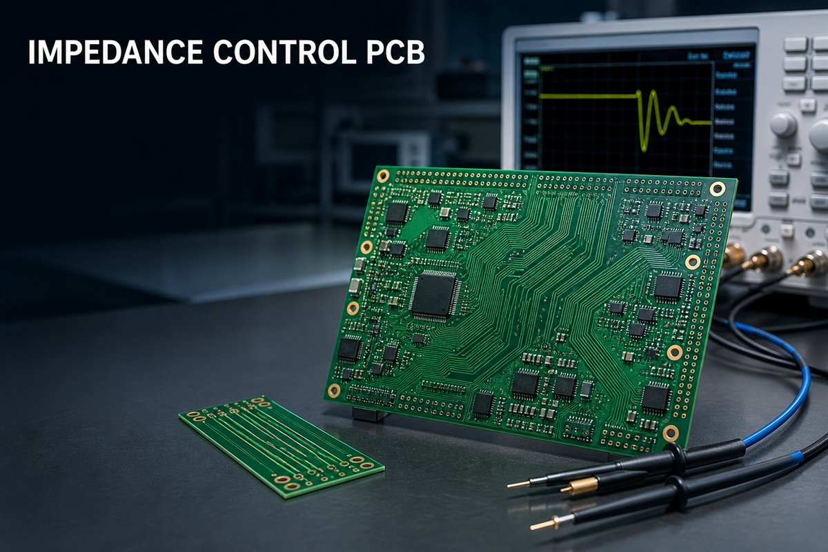
An impedance control PCB has one or more transmission lines manufactured to meet specified characteristic-impedance targets. Common examples include single-ended traces and differential pairs used for high-speed digital, communication, or RF signals.
Impedance is affected by the complete trace environment, not trace width alone. Important variables include:
- Finished trace width and copper thickness
- Spacing within a differential pair
- Distance from the trace to its reference plane
- Dielectric material, thickness, and design Dk
- Solder mask and nearby copper geometry
- Etching and lamination tolerances
A calculator can estimate a starting geometry, but the fabricated result depends on the manufacturer’s actual materials and processes. The released design should therefore identify the required impedance, tolerance, signal layers, reference layers, and controlled nets. The PCB supplier can then compare those requirements with the proposed production stackup.
The customer remains responsible for circuit function, interface requirements, signal-integrity targets, and final design approval. EBest Circuit (Best Technology) can review the released files for PCB manufacturability, coordinate a production stackup, fabricate the boards, and provide agreed impedance-testing evidence.
When Does a PCB Need Impedance Control?
Not every signal trace needs controlled impedance. The decision depends on signal edge rate, interconnection length, interface requirements, acceptable reflection, and the complete electrical path. Clock frequency alone is not enough to make the decision.
Customers should evaluate impedance control when a board includes high-speed digital interfaces, RF paths, fast clock or memory signals, antenna feeds, or other transmission lines whose reflections could reduce operating margin. The applicable component and interface specifications should define the required targets.
Skipping control to reduce board cost can create a larger loss later. Possible consequences include:
- Prototype-to-production performance changes
- Intermittent communication errors
- Reduced eye opening or timing margin
- Excessive ringing, overshoot, or radiated noise
- Repeated layout changes without proof that fabrication was the cause
The practical decision is not simply “high-speed board or ordinary board.” Identify which nets require control, the target for each net group, and the evidence needed for acceptance. Do not mark every trace as controlled when only a small number of critical nets require it; unnecessary requirements can increase engineering work, coupon space, testing, and cost.
PCB Impedance Control Requirements
An RFQ that says only “impedance control required” leaves essential decisions unresolved. Before quotation or engineering release, provide a controlled-impedance table or equivalent fabrication note that connects each target to specific layers and net classes.
The release package should state:
- Target impedance for every controlled net class
- Whether each target is single-ended or differential
- Required tolerance, such as the project-approved percentage or ohmic range
- Signal layer and reference plane for each structure
- Controlled net names or an unambiguous net-class identifier
- Intended finished copper weight or thickness
- Approved material family and any required Dk basis
- Finished board thickness and stackup constraints
- Whether impedance coupons and TDR reports are required
- Whether the manufacturer may adjust trace width or spacing
The Gerber or ODB++ data, fabrication drawing, stackup table, net information, and impedance notes must agree. If one file specifies a 100-ohm differential pair while another calls for 90 ohms, fabrication should stop for clarification rather than rely on an assumption.
Customers should also define the approval path. For example, can the PCB manufacturer compensate a finished trace width to suit its etching process? Can it propose a different prepreg while maintaining the approved dielectric thickness and impedance? Which changes require written customer approval? Resolving these questions before CAM release helps prevent untracked changes and repeated quotation cycles.
Controlled Impedance PCB Layer Stackup
The layer stackup connects the electrical model to the material that will be laminated. A nominal layer count and overall thickness are not enough. The manufacturer needs the copper distribution, core and prepreg construction, finished dielectric thicknesses, material data, and reference-plane relationships.
For each controlled structure, confirm:
- Whether it is a surface microstrip, embedded microstrip, stripline, or coplanar structure
- Which plane provides the continuous reference
- The finished dielectric thickness between the signal and reference layers
- The finished trace width, copper thickness, and differential spacing
- Whether solder mask is included in the calculation
- The material Dk value and frequency basis used for modelling
- Whether nearby copper, plane openings, or routing transitions disturb the structure
A standard stackup can shorten engineering time, but it should not be accepted only because its layer count and board thickness match the design. The available trace geometry must also fit the customer’s routing density and manufacturing limits.
The customer should review the supplier’s proposed production stackup before fabrication. If the supplier changes dielectric thickness or material construction, the calculated line geometry may also need to change. Keep the approved stackup, impedance table, and revised production files under the same revision so purchasing, engineering, and quality teams evaluate one controlled release.

Impedance Control in PCB Manufacturing
Manufacturing converts the approved model into actual copper and dielectric geometry. Lamination, material variation, copper plating, imaging, and etching all influence the finished result. That is why a theoretical value from the design stage cannot, by itself, prove production conformity.
During engineering review, the PCB manufacturer should compare the customer’s targets with the proposed stackup and process capability. If compensation is necessary, the supplier should return the proposed production geometry for approval instead of silently changing controlled features.
Typical manufacturing controls include:
- Material and stackup verification before lamination
- CAM checks for controlled nets, reference planes, and coupon structures
- Process compensation based on the supplier’s qualified etching data
- Finished-copper and geometry control
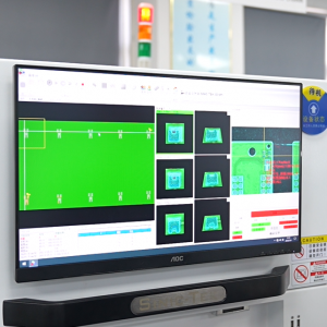
- Coupon fabrication on the same production panel under representative conditions
- TDR measurement against the agreed target and tolerance
- Traceable reporting linked to the job, lot, or panel as agreed
Coupon placement and design should represent the relevant production structures. A coupon is useful only when its layer, reference plane, geometry, materials, and processing are representative of the controlled traces being accepted.
If a measured coupon is outside the specified tolerance, the correct response depends on the agreed acceptance plan. The manufacturer should contain the affected material, review the stackup and process data, and communicate the finding before shipment. The customer should decide whether further investigation, rework, rebuild, or a documented deviation is acceptable.

How to Check Impedance on PCB?
The most common production method is TDR testing of an impedance coupon. The instrument sends a fast electrical transition into the test structure and evaluates reflections along the transmission path. The result is compared with the approved target and tolerance.
Before accepting a test report, check that it identifies:
- Customer part number and revision
- Manufacturing job, lot, or panel reference
- Coupon or test-structure identification
- Controlled structure and target impedance
- Required tolerance or acceptance limits
- Measured result for each reported structure
- Test date, equipment, or method when required by the quality plan
- Clear pass/fail status and authorized review
A report showing only one impedance number without identifying the structure or job may not be sufficient for traceability. Likewise, a passing coupon does not prove the performance of the complete assembled product. It demonstrates that the representative PCB structure met the agreed impedance acceptance criteria.
Customers with stricter reliability or compliance needs should define the sampling plan, report format, retention period, and any coupon-storage requirement in the purchase documentation. If direct board measurements, network analysis, or product-level signal-integrity testing are needed, those requirements should be specified separately because they are not automatically included in standard coupon testing.
A Practical Impedance Control PCB Example
Consider a multilayer control board containing a high-speed differential interface and several single-ended clock lines. The initial RFQ includes Gerber files and an overall board thickness, but it does not identify the controlled nets, reference planes, tolerance, or required report.
If fabrication begins from that package, different suppliers may choose different dielectric constructions and compensate the traces differently. The boards may all match the visible artwork while producing different impedance results.
A safer release would include:
- A table listing each controlled net class and target
- The approved layer and reference-plane assignments
- A preliminary stackup with material and thickness constraints
- Permission boundaries for trace-width or spacing adjustment
- A requirement for representative coupons and a TDR report
- A named customer approver for stackup or geometry changes
EBest Circuit (Best Technology) can review this package against available PCB materials and fabrication rules. If the proposed stackup requires a geometry adjustment, the revised values can be returned for customer approval before production. After fabrication, the agreed coupon results can be supplied with the manufacturing record.
This process does not transfer circuit-design ownership to the manufacturer. It gives both parties a controlled handoff: the customer defines the electrical requirement, the manufacturer defines how the approved requirement will be produced and verified, and unresolved differences are closed before material is committed.
FAQs About Impedance Control PCB
Does every high-speed PCB require impedance control? Not automatically. The customer should evaluate signal edge rate, interconnection length, interface specifications, and acceptable reflection. Control the nets whose transmission-line behaviour can affect performance.
What impedance tolerance should I specify? Use the tolerance required by the interface, design analysis, and product acceptance plan. Confirm that the selected PCB construction and supplier process can support it before release; do not assume one tolerance fits every design.
Can a PCB manufacturer change controlled trace width? Only within the agreed approval process. Manufacturing compensation may be necessary, but the proposed finished geometry and stackup should be reviewed when the change could affect routing, clearance, coupling, or signal performance.
Does a passing TDR coupon guarantee that the assembled product will work? No. It verifies the representative PCB structure against the agreed impedance criteria. Component models, connectors, vias, layout transitions, assembly, firmware, and system conditions still affect final performance.
What should I send for an impedance control PCB quotation? Send the fabrication data, drawing, stackup constraints, controlled-net table, impedance targets and tolerances, material requirements, finished thickness and copper requirements, coupon/report expectations, quantity, and revision. For a manufacturing review or quotation, contact sales@bestpcbs.com.