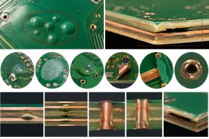
Stop solder mask defects before they become assembly rework. A blocked pad can weaken a joint, a broken mask dam can contribute to bridging, and exposed copper can create a reliability risk.
The fastest path to a decision is to identify what the defect affects, compare it with the released requirement, and request evidence that supports acceptance, repair, or rejection.
What Are Solder Mask Defects?
Solder mask defects are unintended problems with PCB mask coverage, openings, alignment, adhesion, curing, or cleanliness. Common signs include exposed copper, mask on pads, pinholes, bubbles, peeling, cracks, contamination, and broken mask dams.
Do not approve a board from appearance alone. Confirm:
- The affected feature and board location
- The released Gerber and drawing revision
- The number of affected boards
- The applicable acceptance requirement
- Whether the defect appeared before or after assembly
This gives you a faster, evidence-based disposition instead of a subjective appearance debate.
Common PCB Solder Mask Defects
Match the visible problem with the loss you need to prevent:
| What you find | What you can prevent |
|---|---|
| Mask on pads or shifted openings | Weak joints and assembly delays |
| Exposed copper or pinholes | Corrosion and reliability escapes |
| Blisters, peeling, or cracks | Heat-triggered failures during PCBA |
| Broken mask dams | Bridging between fine-pitch pads |
| Via-tenting defects | Solder wicking and uneven surfaces |
| Debris or contamination | Adhesion and cleanliness disputes |
Location matters more than appearance alone. A small mark on unused laminate is not equal to the same defect on a BGA pad, test point, fine-pitch footprint, or closely spaced conductor.
Ask for a marked defect map and quantity count. You can then see whether the issue is isolated, feature-specific, panel-related, or present across the lot.

How Solder Mask Problems Affect Assembly and Reliability
Catch solder mask problems before component placement to avoid sorting populated boards later.
Mask on pads can reduce solderable area. Missing dams can increase bridging risk. Weak or undercured mask may blister, crack, or peel during baking, reflow, wave soldering, cleaning, or repair.
Exposed conductors may also lose protection against moisture and contamination. The actual field risk depends on location, spacing, voltage, cleanliness, and the product environment, so appearance alone cannot predict service life.
Early containment helps you avoid:
- Line stoppage and emergency sorting
- Weak joints or solder bridges
- Damage from late-stage rework
- Shipment delays and repeated lot disputes
Causes of Solder Mask Failure in Design and Fabrication
Separate design, fabrication, and assembly causes before asking for corrective action.
Design data: Incorrect openings, insufficient expansion, unclear via treatment, or mask dams below manufacturing capability can create repeatable defects. Confirm the minimum solder mask sliver the fabricator can hold before releasing fine-pitch data.
Fabrication: Contamination, weak surface preparation, registration error, incorrect processing, or incomplete curing can reduce coverage or adhesion.
Assembly: Excessive heat, incompatible chemistry, fixtures, handling, or repeated rework can damage an otherwise acceptable coating.
Use four checks to reach a decision faster:
| Check | Decision it supports |
|---|---|
| Released files and drawing | Design issue or fabrication issue? |
| Defect map and quantity | Sort, release, or remake? |
| Before/after assembly records | When did the damage occur? |
| Material, cure, and process records | What must change next lot? |
A corrective action should change a file, note, process control, or inspection point. “Pay more attention” does not prevent recurrence.
Simple Tests for Solder Mask Damage
Use agreed tests to obtain release evidence without damaging acceptable boards.
Start with visual inspection under suitable lighting and magnification. Compare the affected area with the same feature on an unaffected board. Record exposed copper, lifted edges, cracked dams, contamination, or color transfer.
Adhesion, hardness, solvent-resistance, or controlled thermal checks may help separate weak adhesion from incomplete curing. When a customer specification calls for IPC-TM-650 testing methods for solder mask, record the exact method number and acceptance limit.
For each test, record:
- Board revision, lot, sample size, and location
- Before-and-after photographs
- Method, conditions, and acceptance limit
- Results from affected and control samples
Electrical test is not a substitute for mask inspection. A board may pass continuity while still creating soldering or protection risks.
What Inspection Evidence Should a Buyer Request?
Replace “the boards are usable” with evidence that supports your decision.
Request:
- Close-up photographs with scale and marked locations
- Lot, panel position, inspected quantity, and defect count
- Confirmation of the released file and drawing revision
- The applicable acceptance requirement
- Test method and actual result
- Containment status and proposed disposition
- Root cause and corrective action for repeat defects
For repairs, also approve the material, area, cure method, final thickness, and post-repair inspection. A repair is useful only when it restores protection without reducing pad area or creating a new assembly problem.

A Project Example: Reject, Repair, or Release?
Fine-pitch pads show mask encroachment one day before assembly. Releasing the lot risks poor wetting; rejecting every board may create unnecessary delay.
The buyer quarantines the lot and requests a defect map, measurements, file-revision confirmation, and panel-position data. The results show correct Gerber data but a repeatable registration shift in one panel position.
The evidence supports a controlled decision:
- Release verified unaffected boards
- Reject or remake boards outside the limit
- Repair only with customer approval
- Add a targeted registration check for the next lot
This illustrative example shows the customer benefit: contain first, identify the affected population, and avoid both unsafe release and unnecessary total-lot rejection.
How to Prevent Solder Mask Issues From Repeating
Confirm mask requirements before production so defects do not reach assembly.
Provide synchronized copper, solder mask, drill, and drawing data. State the mask color, finish, via treatment, acceptance standard, and any special thickness or appearance limits.
For dense BGA, fine-pitch, via-in-pad, test-point, and edge-contact areas, request a focused DFM review before releasing the order.
With EBest Circuit (Best Technology), you can confirm solder mask openings, dams, via treatment, and other manufacturability risks before they become assembly rework. You can also coordinate PCB fabrication, PCBA, and agreed inspection evidence with one manufacturing team.
Send previous defect photographs and corrective-action requirements with your RFQ. This directs the review toward the loss you want to prevent. The customer remains responsible for approved design requirements, product-level reliability targets, regulations, and final acceptance.
FAQs About Solder Mask Defects
Can a PCB with solder mask defects still be used? Possibly. Release it only after checking the affected location, quantity, drawing requirement, and assembly risk.
What causes solder mask to peel? Common causes include contamination, poor surface preparation, incomplete curing, heat, incompatible chemistry, or mechanical damage.
Can solder mask over a pad be repaired? Only when the customer approves the method and the repair restores the required solderable area without creating new damage.
Which files help prevent solder mask defects? Provide synchronized Gerbers, drill files, a fabrication drawing, revision notes, via instructions, and acceptance requirements.
What should I send for a solder mask review? Send the approved PCB files, fabrication notes, defect photographs, lot information, and inspection requirements to sales@bestpcbs.com.