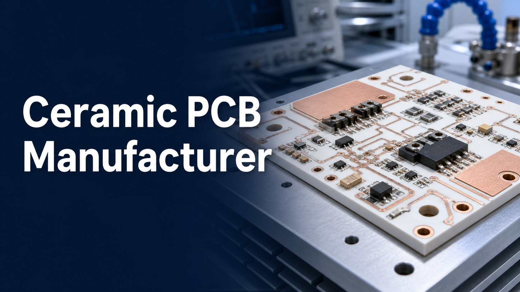
A ceramic PCB manufacturer should help you choose the right substrate, ceramic process, copper structure, surface finish, DFM limits, assembly path and test plan before you place the order. Ceramic boards are not selected only because they look more advanced than FR4. They are used when heat, insulation, high temperature, power density, RF behavior, dimensional stability or long-term reliability makes an organic laminate a poor fit.
EBest Circuit supports buyers with ceramic PCB manufacturing, DFM review, material and process confirmation, optional ceramic PCB assembly, BOM/CPL review and RFQ planning. Send your Gerber or ODB++, drawing, stackup, substrate request, copper requirement, finish, quantity, assembly files and test needs early so the project can be reviewed as a ceramic substrate build rather than a normal PCB quote.
Ceramic Board Buyer Decision Before Quote Approval
A ceramic PCB manufacturer should first help you decide whether the project needs alumina, aluminum nitride, ZTA, silicon nitride, DPC, DBC/DCB, AMB, thick film, LTCC or HTCC. The right answer depends on heat flow, conductor thickness, layer count, operating environment, part mounting, dimensional limits and cost target.
Many ceramic PCB delays happen because the RFQ says only “ceramic PCB” without defining the substrate and process. That is not enough. A thin film ceramic circuit, a DPC board, a DBC/DCB power substrate and an AMB ceramic board do not follow the same design rules or quote logic.
Is your ceramic PCB quote difficult to compare because every supplier is reading the files differently?
Buyers often run into these problems before a ceramic PCB order is approved:
- The project asks for a ceramic PCB, but the substrate material and ceramic process are not clearly tied to the thermal or electrical requirement.
- The copper thickness looks attractive in a quote, but trace width, spacing, panel size, edge quality and assembly clearance have not been reviewed together.
- The board needs good heat transfer, yet the RFQ does not show the heat source, heat path, mounting surface or expected test condition.
- The same design is sent to FR4, MCPCB and ceramic PCB suppliers without adjusting design rules, creating slow DFM loops.
- Assembly, component sourcing and test requirements arrive after fabrication planning, forcing late changes to pads, finish, fixtures or packaging.
Five RFQ Details That Change a Ceramic Board Build
Ceramic PCB projects often get delayed when the purchase team compares unit prices before engineering has confirmed the substrate, conductor, finish and test scope. A low line-item price can hide a weak quote if the supplier has not checked manufacturability.
For a buyer, the fastest path is to make the quote package specific. Show where the heat enters the ceramic substrate, which components sit on high-copper areas, whether the board needs assembly, which finish is expected, and what inspection or reliability checks are important for the application.
EBest Circuit helps turn ceramic PCB uncertainty into a reviewable RFQ package:
- We review substrate choice, ceramic process, copper thickness, line/space, hole design, finish and board outline together instead of quoting one isolated specification.
- We separate standard capability, special review items and file-dependent limits so buyers do not approve a quote on unsupported assumptions.
- We connect ceramic PCB fabrication with PCBA planning when pads, power devices, thermal interfaces, component sourcing or test fixtures affect the finished product.
- We help buyers compare quote scope, not only unit price, so prototype and production decisions are easier to defend internally.
EBest Circuit Review Path for Ceramic Substrate Orders
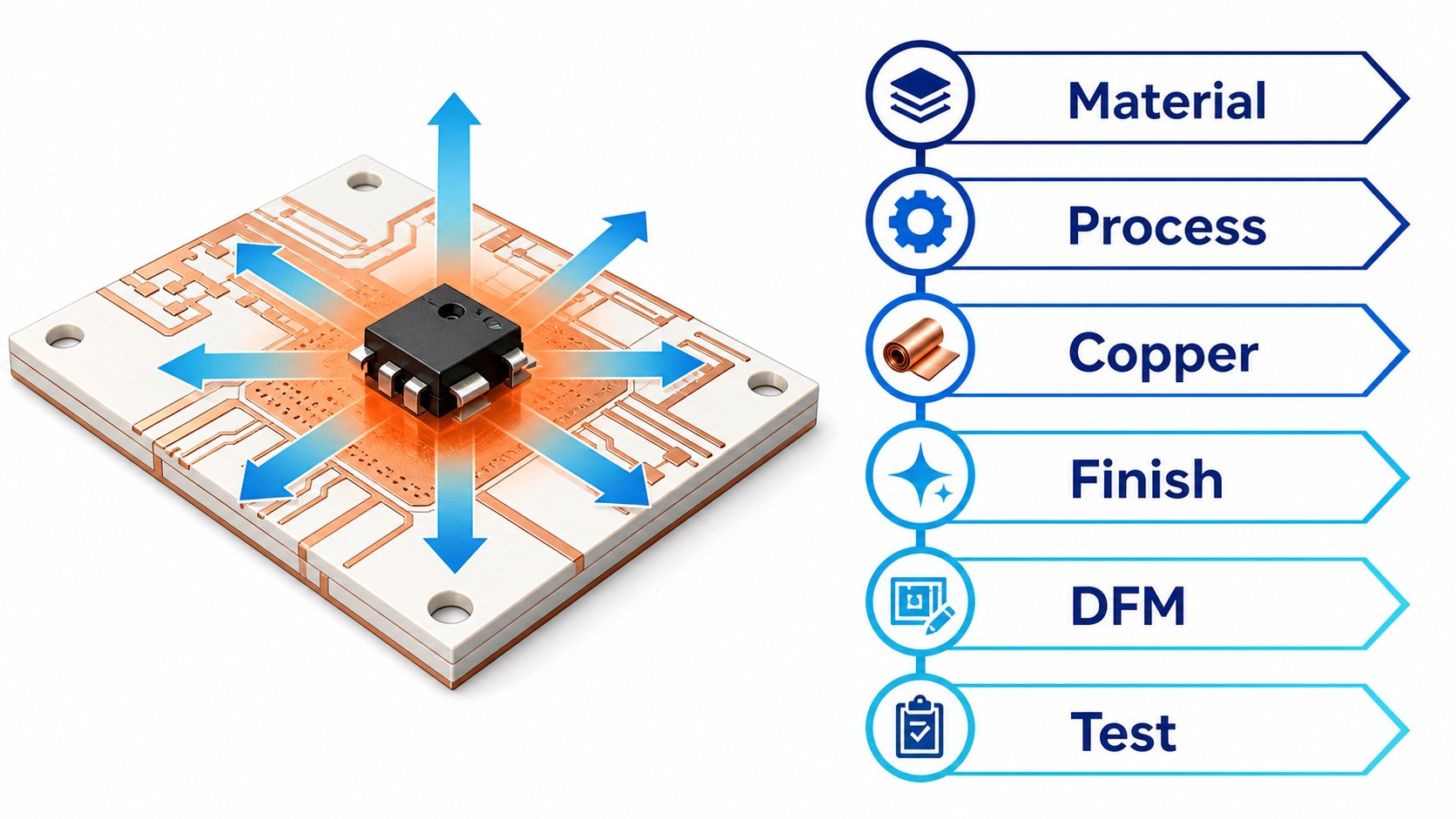
EBest Circuit reviews ceramic PCB projects by checking substrate, process, copper, geometry, finish, assembly and test requirements before production planning. This reduces the chance that a quote looks acceptable but later fails during DFM, assembly or reliability review.
For example, a high-power ceramic board may need DBC/DCB ceramic PCB or AMB discussion because conductor thickness and heat transfer are more important than fine traces. A precision circuit may need DPC or thin film review because line/space, metallization and surface quality matter more. The right manufacturing route should be selected from the function of the board, not from a catalog word.
Ready to Review a Ceramic PCB Build?
Send your substrate choice, Gerber or ODB++, drawing, copper requirement and assembly scope for a practical DFM and RFQ review.
DFM review | BOM/CPL check | Fabrication and assembly planning
When Ceramic Beats FR4 or Metal Core PCB
Ceramic PCB is usually the right choice when the board needs stronger heat transfer, electrical insulation, dimensional stability or high-temperature performance than a normal FR4 board can provide. It is not the lowest-cost route for every circuit, but it can be the better route when thermal or reliability risk dominates the project.
| Project Need | Why Ceramic PCB May Fit | What to Confirm Before RFQ |
|---|---|---|
| High heat density | Ceramic substrates can support strong heat transfer paths. | Heat source, substrate, copper thickness and mounting method. |
| Power electronics | DBC/DCB or AMB structures can support thicker conductors. | Copper weight, isolation, outline, finish and test needs. |
| RF or high-frequency circuit | Some ceramic materials offer stable dielectric behavior. | Material, impedance target, geometry and finish. |
| Harsh or high-temperature environment | Ceramic substrates can provide heat and chemical stability. | Operating temperature, coating, metallization and reliability checks. |
Alumina, AlN, ZTA and Si3N4 Board Fit
Ceramic PCB material should be selected from thermal, mechanical, electrical and cost requirements, not from the keyword alone. Verified EBest Circuit capability records list ceramic substrate options including Al2O3, AlN, ZTA and Si3N4. Special substrate discussions may also involve glass, quartz, sapphire and different alumina grades depending on the project.
Alumina is common in ceramic circuit projects because it balances insulation, availability and cost. Aluminum nitride is often considered when thermal performance is a bigger driver. ZTA and silicon nitride can enter the discussion when mechanical strength, hardness or stability matter. Each choice should be checked with board thickness, conductor method, outline and test requirements.
DPC, DBC, AMB, Thick Film, LTCC and HTCC Routes
The ceramic PCB process should match the required copper structure, layer count, thermal path and operating environment. The source capability records include DPC, DBC/DCB, AMB, thick film, LTCC and HTCC, but they are not interchangeable processes.
| Process | Typical Buying Question | RFQ Evidence Needed |
|---|---|---|
| DPC | Do I need finer ceramic circuit features? | Line/space, conductor thickness, finish and dimensional drawing. |
| DBC/DCB | Do I need a strong direct copper thermal path? | Copper thickness, substrate, isolation, power device location. |
| AMB | Do I need a robust ceramic power substrate? | Substrate, copper thickness, outline, reliability expectation. |
| Thick film, LTCC or HTCC | Does the design need a ceramic circuit route beyond common DPC/DBC? | Layer count, conductor material, application conditions and drawings. |
Layer Count and Panel Size by Ceramic Route
Layer count, copper thickness and panel size must be checked by ceramic process because one capability number cannot represent every ceramic PCB route. EBest Circuit’s English capability source lists thin film ceramic PCB up to 10 layers, while DBC/DCB, DPC and AMB are listed as 2-layer processes in that table.
The same source lists example maximum panel sizes of 200 x 200 mm for thin film ceramic PCB, 138 x 178 mm for DBC/DCB, 138 x 190 mm for DPC and 114 x 114 mm for AMB. These figures should be treated as process-specific review data, not as a universal promise for every ceramic board.
| Capability Item | Verified Process-Specific Data | Buyer Action |
|---|---|---|
| Layer count | Thin film up to 10 layers; DBC/DCB, DPC and AMB listed as 2 layers in the English table. | Send stackup and process expectation for review. |
| Conductor thickness | Thin film 5-13 um; DPC 2-200 um; DBC/DCB 3.9-8.6 oz; AMB 8-22.9 oz. | Confirm whether the project needs fine features or heavy current paths. |
| Panel size | Panel limits vary by process and must be checked against the drawing. | Provide board outline, panel needs and quantity. |
Trace, Space, Drill and Thickness Limits
Ceramic PCB geometry should be reviewed before quote approval because trace/space, hole size and substrate thickness depend on process and material. Verified capability records list thin film and DPC minimum trace/space as 6/8 mil, DBC/DCB as 12/12 mil and AMB as 20/20 mil in the English ceramic table.
The broader ceramic process source also lists general line width and line spacing at 0.1 mm / 0.1 mm, with 0.076 mm / 0.076 mm as a special process item. It lists minimum PTH and NPTH as 0.05 mm and a PTH aspect ratio of 5:1. These values should be checked against your drawing, finish and process route before they are used for approval.
Pad Finish Choices for Soldering, Contact or Bonding
Surface finish affects solderability, wire bonding, storage, assembly and contact reliability, so it should be confirmed before the ceramic PCB quote is finalized. EBest Circuit’s ceramic capability source lists OSP, ENIG, immersion silver, immersion tin, ENEPIG and hard gold among available surface treatment options.
Do not select finish only from price. Ask whether the finish matches your component package, assembly method, contact requirement, storage condition and test plan. If a ceramic PCB will be assembled later, the finish decision should be made together with the PCBA requirement.
DFM Review Before Ceramic Files Move to CAM
A useful ceramic PCB DFM review checks whether the selected material, process, copper, geometry, finish and test plan can be built together. The review should happen before purchasing, because changing ceramic process after quote approval can change cost, lead time, inspection and assembly planning.
For a practical review, send the Gerber or ODB++ files, drill data, board drawing, stackup, copper requirement, substrate requirement, surface finish, application notes and any thermal or electrical constraints. If the design is moving from FR4 or MCPCB to ceramic PCB, call out what failed or what performance target changed.
Component Mounting and Thermal Interface Planning
Ceramic PCB assembly should be planned together with fabrication when component pads, heat-generating devices, soldering, sourcing or test fixtures affect the final product. A ceramic substrate can move heat well, but the assembled product still depends on package selection, solder joints, thermal interface, mechanical mounting and inspection.
EBest Circuit can review fabrication and assembly needs together when you provide Gerber/ODB++, BOM, CPL, assembly drawing, quantity and test requirements. This is especially useful for LED modules, power devices, sensor modules, high-temperature electronics and compact thermal designs.
Reliability Checks for Ceramic Boards Under Load
Testing for ceramic PCB orders should match the failure risks of the application rather than follow a generic checklist. Dimensional inspection, visual inspection, electrical test, finish checks, thermal review and assembly inspection may all matter depending on the board.
If the ceramic board carries power or heat, ask how the supplier will confirm critical copper areas and insulation. If the board supports precision signals, ask how the geometry, finish and cleanliness will be checked. If the board is assembled, define whether AOI, X-ray, functional test or custom fixture testing is required.
High-Temperature and Chemical Environment Review
Environment review matters because ceramic PCB projects are often selected for heat, corrosion resistance or stability under tougher operating conditions. Tell the manufacturer whether the board will face high ambient temperature, aggressive cleaning, chemical exposure, outdoor sealing, power cycling or continuous heat from mounted devices.
This information helps the engineering team review substrate, finish, copper, mounting and inspection needs together. A ceramic board that works on a bench may still need a different finish, coating, fixture plan or acceptance test when it is used in a harsher product environment.
Isolation, Creepage and Grounding Concerns
Isolation and creepage should be reviewed early when ceramic PCB is used in power, RF or high-voltage electronics. Ceramic can provide strong insulation, but the final circuit still depends on conductor spacing, pads, vias, metallization, surface condition and assembled component clearance.
Share voltage, current, isolation targets and any safety spacing rules with the RFQ. Do not assume that a ceramic substrate alone solves all electrical clearance issues. The layout and assembly both need to support the same requirement.
Mounting Flatness, Edge Chipping and Ceramic Handling
Ceramic boards need mechanical handling review because the substrate is rigid and can be sensitive to edge stress, mounting force and packaging choices. Outline shape, hole placement, panelization, screw pressure and fixture design can affect the real manufacturing plan.
If the board will be mounted against a heat sink, metal frame or optical housing, send the mechanical drawing with the PCB files. This helps the supplier check flatness, keep-out areas, edge clearance and safe handling before production begins.
Power Module, LED and Sensor Application Fit
Ceramic PCB is often considered for power modules, LED thermal boards, sensors, RF circuits and compact electronics where heat or stability drives the design. The application should guide the ceramic process and quote scope.
A power device may need conductor thickness and heat-spreading review. An LED module may need thermal path, surface finish and assembly review. A sensor or RF circuit may need tighter geometry, clean finish and stable material behavior. These are different buyer problems, even when they all use ceramic substrates.
Failure Modes: Copper Lift, Cracking and Hot Spots
Common ceramic PCB risks include weak copper adhesion, substrate cracking, local hot spots, finish mismatch and late assembly changes. These risks are easier to control before the files move into production than after a sample fails inspection.
Ask the supplier to review copper thickness, conductor geometry, ceramic thickness, device location, heat path and mechanical mounting together. If the design has high power density, note which areas are most critical so the DFM review does not treat all copper features equally.
Supplier Questions to Ask Before Purchase Order
Ask ceramic PCB suppliers questions that reveal whether they understand your specific build, not only whether they can quote a material name. Useful questions include which process route they recommend, which dimensions require review, how copper thickness affects line/space, what finish they suggest for assembly, and which test records can be provided.
Also ask what information is missing from your RFQ. A strong supplier should be able to tell you what must be confirmed before the quote is reliable.
RoHS, UL and IPC Documents to Confirm
Compliance documents should be confirmed from the actual order scope instead of assumed from a generic ceramic PCB listing. If your product requires RoHS, UL-related documentation, IPC acceptance criteria, material declarations or customer-specific records, state that in the RFQ.
Do not let certification wording float in the quote without a document requirement. If a document is needed for your customer approval process, ask for it before purchase order release and confirm whether it applies to the quoted process.
Ceramic PCB Checklist Before Releasing the Order
Before releasing a ceramic PCB order, check whether the quote covers substrate, process, copper, finish, geometry, assembly, testing and documentation. This checklist prevents the most common gap: a price is approved before the build is fully defined.
- Substrate and ceramic process are clearly stated.
- Copper thickness and critical heat path are reviewed.
- Line/space, holes, board size and substrate thickness match the selected route.
- Finish matches soldering, contact or bonding needs.
- Assembly, sourcing and test scope are included if required.
- Required documents and acceptance criteria are named in the RFQ.
What Ceramic Board Buyers Need to Solve
Most ceramic board buyers are trying to solve a specific performance risk, not simply buy a different PCB base material. The risk may be heat concentration, insulation distance, power cycling, signal stability, device mounting, high-temperature operation or a product approval requirement.
State that problem directly in the RFQ. A supplier can give a more useful review when the files explain what the ceramic board must protect, improve or replace in the final product.
Cracking and Delamination Root Cause Review
Cracking and delamination risk should be reviewed when ceramic boards face mechanical stress, thermal cycling or uneven mounting pressure. Ceramic substrates are strong in the right design, but they should not be treated like flexible laminate during handling, assembly or enclosure design.
Tell the manufacturer where the board is clamped, how it is supported, which components add local stress and whether the product will see repeated heating and cooling. These details can change edge clearance, panel handling, fixture planning and inspection focus.
Need Ceramic PCB Fabrication and Assembly Together?
EBest Circuit can review board files, BOM, CPL, substrate choice, finish and test needs in one RFQ package.
Ceramic substrate | Copper and finish | PCBA planning | Test requirements
Price Drivers Buyers Should Normalize
Ceramic PCB cost is mainly driven by substrate, process route, copper thickness, layer count, size, finish, tolerance, quantity, assembly and test requirements. A quote that does not define these items is hard to compare.
| Cost Factor | Why It Changes the Quote | How to Control It |
|---|---|---|
| Substrate and process | Alumina, AlN, DPC, DBC/DCB and AMB use different manufacturing routes. | Choose from the actual heat, insulation and copper requirement. |
| Copper and geometry | Thicker copper and tighter line/space can change yield and process review. | Send current path, drawing and design rules early. |
| Finish and assembly | Finish must match soldering, contact or bonding needs. | Share BOM, CPL and assembly plan before quote approval. |
| Testing and reliability | Extra inspection or custom test fixtures add scope. | Define acceptance criteria in the RFQ. |
Supplier Shortlist Criteria for Ceramic Boards
Compare ceramic PCB manufacturers by how clearly they review your material, process, copper, finish, assembly and test requirements, not by price alone. A strong supplier should help you see what is standard, what is special and what must be confirmed from the files.
- Can the supplier explain which ceramic process fits your application?
- Can the supplier review copper thickness, trace/space, holes and panel size together?
- Can the supplier support both bare ceramic PCB and assembly if your project needs PCBA?
- Can the supplier give DFM feedback before purchase order approval?
- Can the supplier help define test and inspection scope instead of leaving it vague?
- Can the supplier separate confirmed capability from file-dependent review items?
File Package for a Fast Ceramic Board Review
A ceramic PCB RFQ should include the files and decisions needed to confirm the board as a ceramic substrate project. The more complete the package is, the easier it is to avoid re-quotation and late engineering changes.
- Gerber or ODB++ files.
- Drill files and mechanical drawing.
- Substrate request, such as alumina, AlN or project-specific review.
- Preferred process if known, such as DPC, DBC/DCB, AMB, thick film, LTCC or HTCC.
- Copper thickness or conductor requirement.
- Board thickness, outline, panel or array requirements.
- Surface finish requirement.
- BOM, CPL and assembly drawing if PCBA is needed.
- Quantity, prototype or production stage and target schedule.
- Thermal, electrical, insulation, reliability or test requirements.
Why Put EBest Circuit on the Quote List Early?
EBest Circuit belongs on your ceramic PCB quote list when you need engineering review, cost control, fabrication planning, optional PCBA support and clear RFQ feedback before production starts. We do not ask buyers to send a vague “ceramic PCB” request and wait for a price. We help define the build so the quote can be compared on scope and risk.
That matters for buyers in power electronics, LED, industrial control, communication modules, medical electronics, sensors and compact thermal assemblies. The supplier you choose should help you protect the project from material mismatch, unsupported geometry, finish errors, assembly surprises and unclear test scope.
FAQ About Ceramic PCB Manufacturers
These questions help buyers clarify ceramic PCB scope before asking for a quote.
What is a ceramic PCB manufacturer?
A ceramic PCB manufacturer builds circuit boards or substrates using ceramic materials instead of standard organic laminate. The manufacturer should help confirm substrate, ceramic process, copper, surface finish, geometry, assembly and testing requirements before production.
Is ceramic PCB better than FR4?
Ceramic PCB is better than FR4 when the project needs stronger thermal performance, electrical insulation, dimensional stability or high-temperature behavior. FR4 may still be more cost-effective for standard electronics without severe heat or reliability requirements.
What is the difference between DPC and DBC ceramic PCB?
DPC and DBC/DCB are different ceramic metallization and copper bonding routes. DPC is often considered where finer circuit features are important, while DBC/DCB is often considered for stronger copper and thermal power paths. The right choice depends on your design files and application.
Can ceramic PCB be assembled with components?
Yes, ceramic PCB can be assembled when the pads, finish, component package, soldering method and inspection plan are suitable. Send BOM, CPL, assembly drawing and test requirements with the fabrication files so the assembly scope can be reviewed early.
What files are needed for a ceramic PCB quote?
Send Gerber or ODB++, drill files, mechanical drawing, substrate request, copper requirement, finish, quantity, target schedule and any thermal or electrical test needs. If assembly is required, also send BOM, CPL and assembly drawings.
Final Recommendation
Choose a ceramic PCB manufacturer that can review the complete project, not only quote a ceramic material name. Your quote should connect substrate, process, copper, finish, DFM, assembly and testing so the board can move from prototype to production with fewer surprises.
To review a ceramic PCB project with EBest Circuit, send your Gerber or ODB++, drawing, stackup, substrate preference, copper thickness, surface finish, BOM, CPL, quantity, test requirements and target schedule to sales@bestpcbs.com. Our team will help check the files, confirm the manufacturing route and prepare a practical quotation scope.
You may also like








Tags: ceramic PCB, PCB Quote, Thermal PCB