If you’ve worked with high-frequency circuits or sensitive signals, you might have come across the term “impedance control.” Understanding and managing impedance can be the difference between a reliable design and one plagued by signal loss or interference.
Are You Facing These Challenges?
Many customers come to us after struggling with unstable signal performance, failed first builds, or mismatched stack-up assumptions.
Common Challenges
- Signal reflection in high-speed traces
- Differential pair mismatch
- Unclear stack-up planning
- Unexpected impedance deviation after fabrication
- EMI issues caused by routing inconsistency
- Difficulty finding a manufacturer that understands impedance requirements
Our Solution
We help review your layer structure, material selection, and trace geometry before production. With manufacturing-aware engineering support, we reduce the gap between design calculation and actual fabrication result.
Why Choose EBest Circuit for Impedance Control PCB?
Choosing the right manufacturer is important because controlled impedance is not only a calculation task. It is also a process control task. A good supplier needs to understand both design intent and manufacturing consistency.
What We Offer
- Engineering support for stack-up review
- Controlled impedance trace calculation support
- Stable multilayer lamination process
- In-process impedance monitoring
- Support for high-speed and RF PCB projects
- Fast prototype and production service
- PCB and PCBA one-stop support
Our team works closely with customers during the early design stage to reduce risk before fabrication starts. That helps shorten revision cycles and improve project efficiency.
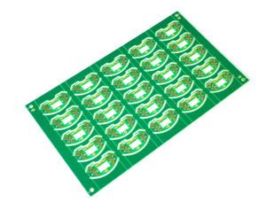
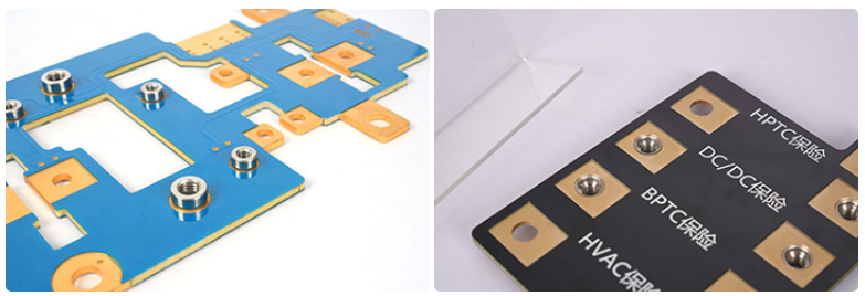
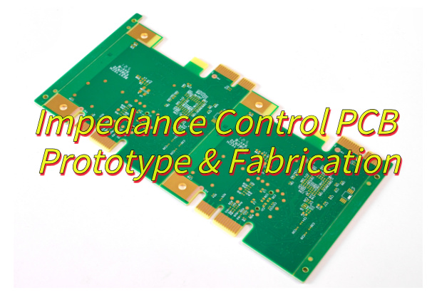
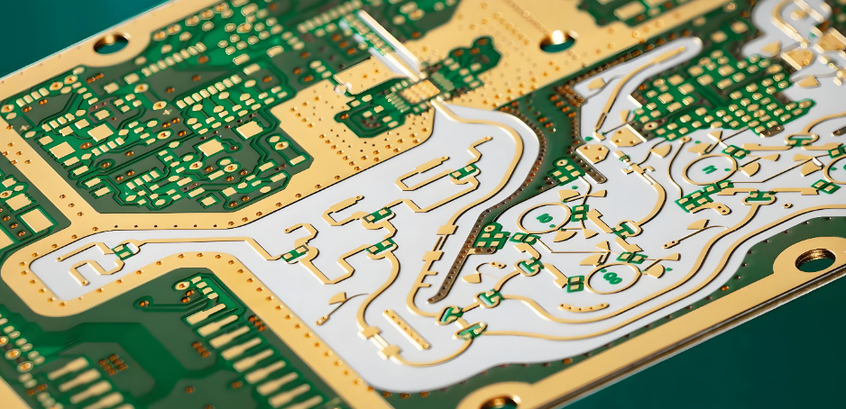
Impedance Control PCB Manufacturer
What is Impedance?
Impedance, in simple terms, is the opposition a circuit offers to the flow of alternating current (AC). It combines two elements: resistance, which is straightforward opposition, and reactance, which is the opposition due to capacitance and inductance. Together, they form impedance, usually measured in ohms (Ω).
In a PCB, impedance is vital because it affects how signals propagate through the traces. If the impedance isn’t controlled, it can lead to reflections, signal loss, or even total communication failure, especially in high-speed circuits.
What is Impedance Control PCB?
An impedance control PCB is a printed circuit board designed so that specific traces maintain a target impedance value throughout signal transmission. The purpose is to make sure signals travel with minimal loss, reflection, or distortion.
In PCB design, impedance is influenced by resistance, capacitance, and inductance. When signal speed rises, these factors become more critical. If impedance changes unexpectedly along the routing path, the signal quality can drop quickly. This is why controlled impedance is widely used in RF circuits, high-speed digital interfaces, and precision analog systems.
Common controlled impedance types include:
- 50Ω single-ended impedance
- 75Ω single-ended impedance
- 90Ω differential impedance
- 100Ω differential impedance
- 120Ω differential impedance
The right target depends on your interface standard, material system, stack-up, and routing method.
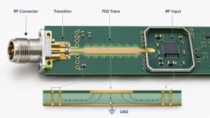
Why Is Controlled Impedance Important in PCB Design?
Controlled impedance matters because signal integrity depends on consistency. In high-speed designs, the copper trace is not just a conductor. It behaves like a transmission line. If the impedance of that transmission line does not match the system requirement, part of the signal energy reflects back toward the source.
This can lead to:
- Signal reflection
- Timing instability
- Crosstalk
- EMI problems
- Higher bit error rates
- Reduced communication reliability
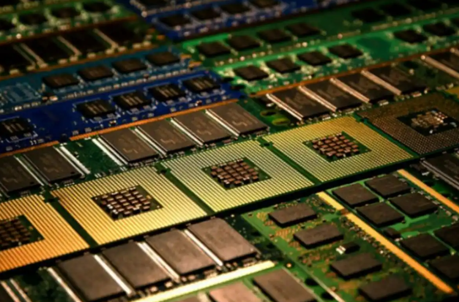
For products using DDR memory, RF modules, antennas, automotive communication, industrial control, or high-speed connectors, impedance control is often not optional. It is part of the design foundation.
What Factors Affect PCB Impedance?
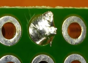
PCB impedance is not determined by one variable alone. It comes from the interaction of conductor geometry, laminate properties, and layer arrangement. Even a small change in fabrication can affect the final result.
1. Trace Width
Trace width is one of the most direct factors. A wider trace usually lowers impedance, while a narrower trace increases it. This is why impedance traces cannot be adjusted casually during layout optimization.
2. Copper Thickness
Copper thickness changes the effective conductor shape and resistance. Thicker copper can reduce impedance, but it also changes etching behavior and production tolerance.
3. Dielectric Constant (Dk)
The dielectric constant of the laminate affects electric field distribution and capacitance between the trace and reference plane. FR4 materials commonly show Dk values around 3.9 to 4.5, while PTFE materials are lower and often preferred for high-frequency applications.
4. Dielectric Thickness
The spacing between the signal trace and the reference plane has a strong effect on impedance. A thicker dielectric usually increases impedance, while a thinner dielectric lowers it.
5. Loss Tangent
Low-loss materials preserve signal energy better, especially in RF and high-speed applications. While loss tangent is not the only parameter that matters, it strongly affects real-world transmission quality.
6. Trace Coupling and Crosstalk
When traces are too close, coupling can change the expected impedance and create crosstalk. This is particularly important in dense differential pair routing.
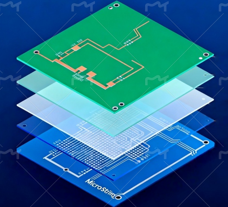
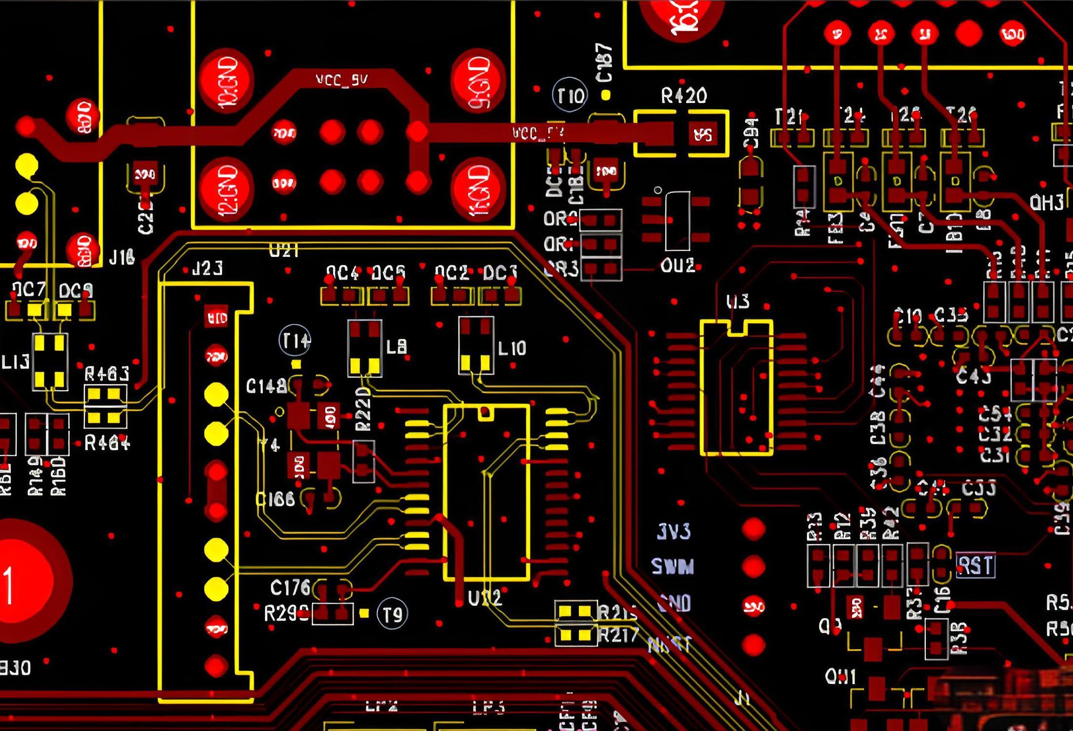
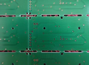
7. Layer Stack-Up
In multilayer PCBs, impedance depends heavily on stack-up design. Signal layer position, plane continuity, dielectric thickness, and via transitions must all be considered together.
When Do You Need an Impedance Control PCB?
Not every board needs controlled impedance. For low-speed, low-frequency, or simple power control products, standard PCB design may be enough. But if your design includes fast signals or strict waveform requirements, controlled impedance becomes much more important.
You should consider impedance control for:
- RF and microwave circuits
- High-speed digital interfaces
- DDR memory routing
- USB, HDMI, PCIe, LVDS, and Ethernet designs
- Differential pair signal routing
- Sensitive analog signal paths
- Long trace interconnects
- Multi-layer signal-dense boards
In these applications, controlled impedance helps maintain cleaner transmission and more predictable electrical behavior.
What Is the Typical Impedance Tolerance of PCB?
Impedance tolerance refers to the acceptable variation between the target impedance and the actual measured result. In many PCB applications, the typical tolerance is ±10%. For more demanding products, tighter tolerances such as ±5% or even ±2% may be required.
A tighter tolerance usually requires:
- More accurate material data
- Better etching control
- Stable lamination process
- Precise stack-up construction
- Reliable impedance coupon testing
This is why the manufacturer’s process capability matters just as much as the design itself.
How Is 100Ω Differential Impedance Controlled?
For 100Ω differential impedance, the process usually begins with stack-up definition and field-solver calculation. The dielectric thickness between layers, line width, and trace spacing must all be matched to the target value. Your original content provided example geometries for four different stack-up options, showing that trace width and spacing vary depending on the specific layer structure.
Example reference values include:
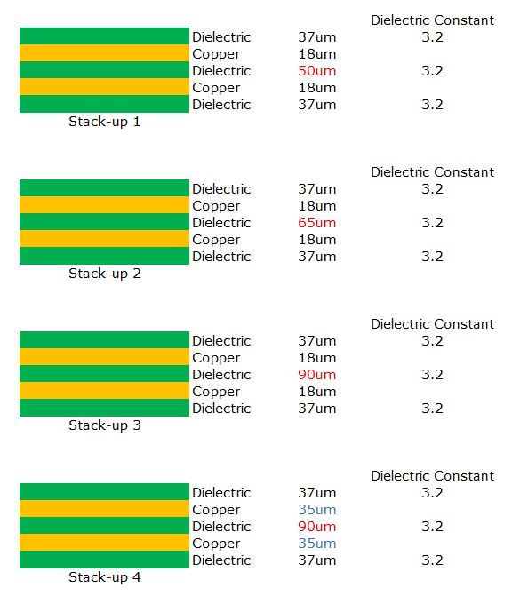
- Stack-Up 1: 70/130μm trace/space
- Stack-Up 2: 95/140μm trace/space
- Stack-Up 3: 125/130μm trace/space
- Stack-Up 4: 105/150μm trace/space
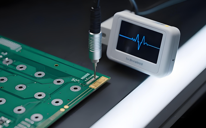
During production, manufacturers normally establish process parameters after first article verification, then carry out random impedance checks during production and on finished boards.
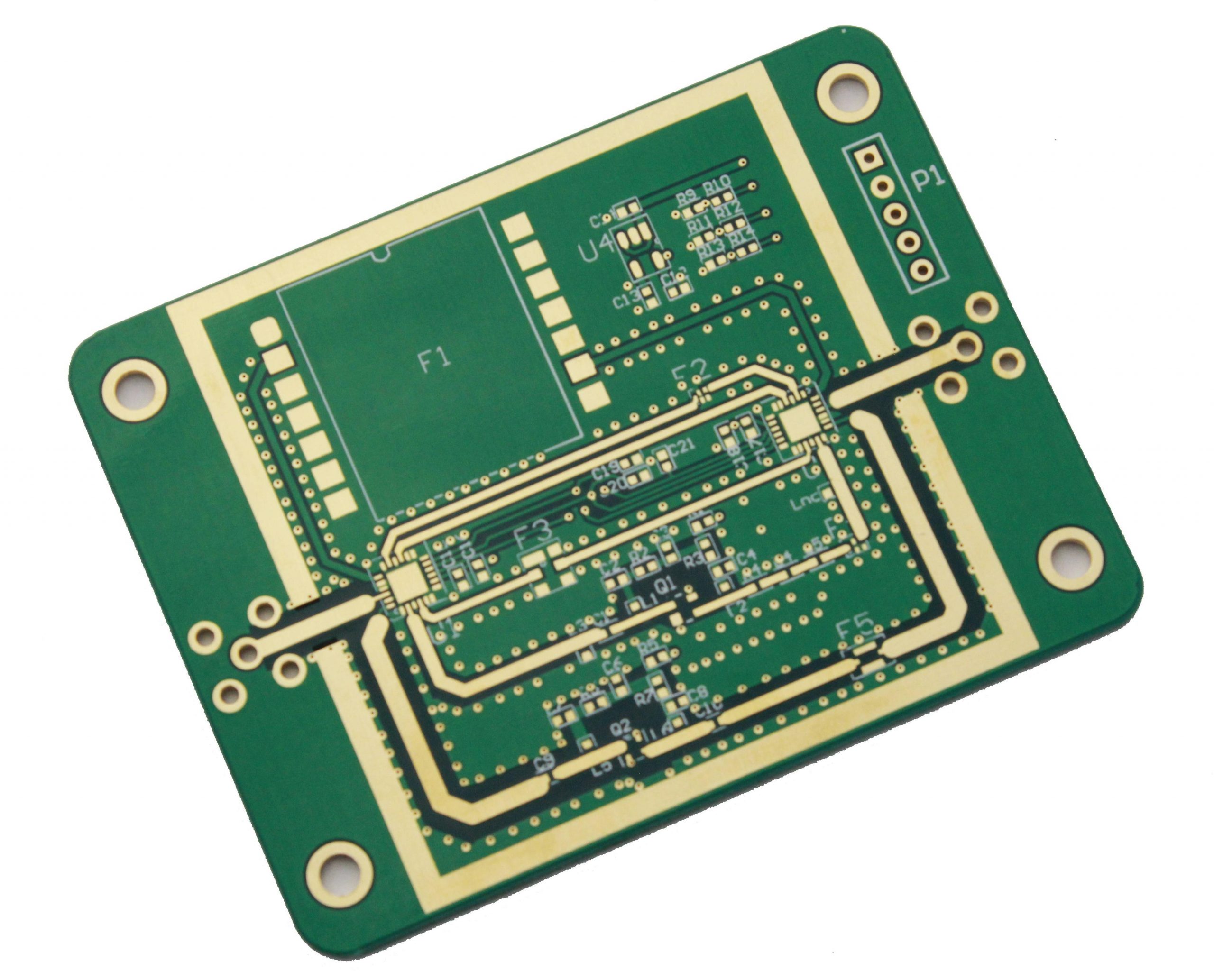
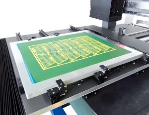
Manufacturing Capabilities for Impedance Control PCB
At EBest Circuit (Best Technology), we support controlled impedance PCB manufacturing for a wide range of applications, from prototype builds to volume production.
Typical Capability Overview
| Item | Capability |
| Board Type | Rigid PCB, multilayer PCB, HDI PCB, RF PCB |
| Layer Count | 1–32 layers typical |
| Controlled Impedance Type | Single-ended and differential |
| Common Target Values | 50Ω / 75Ω / 90Ω / 100Ω / 120Ω |
| Base Materials | FR4, high-speed materials, RF laminates |
| Copper Thickness | Standard to heavy copper options |
| Impedance Verification | Coupon testing / in-process control |
| Application Support | RF, telecom, automotive, industrial, medical |
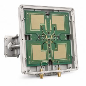
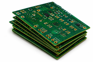
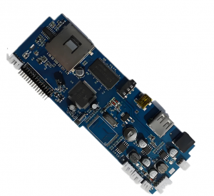
Applications of Impedance Control PCB
Controlled impedance PCBs are widely used in products where signal integrity matters.
Typical applications include:
- Communication equipment
- RF modules
- Automotive electronics
- Medical devices
- Industrial control systems
- Network hardware
- Embedded computing platforms
- High-speed data transmission systems
As product speed and complexity continue to rise, controlled impedance is becoming a standard requirement in more electronic categories.
FAQs About Impedance Control PCB
1. What is the difference between impedance control and standard PCB design?
Standard PCB design may not define a strict trace impedance target. Impedance control PCB design requires specific trace width, spacing, material selection, and stack-up planning to achieve a defined impedance value.
2. Is FR4 suitable for impedance control PCB?
Yes. FR4 can be used for many controlled impedance applications, especially common digital designs. For higher frequencies or lower signal loss requirements, specialized materials may be a better choice.
3. What is the most common differential impedance value?
100Ω differential impedance is one of the most common targets, especially for many high-speed signal interfaces.
4. Can impedance control PCB reduce EMI?
Yes. Stable impedance routing can reduce reflections and signal discontinuities, which helps improve overall signal integrity and can support better EMI performance.
5. How is impedance tested during manufacturing?
Manufacturers commonly use impedance coupons and random process checks during production, followed by finished board verification.
6. What tolerance is usually acceptable?
A typical impedance tolerance is ±10%, while tighter requirements such as ±5% may be used in more demanding applications.
Get a Quote for Your Impedance Control PCB Project
If you are developing a high-speed or RF product, controlled impedance should be considered early in the design stage. A correct stack-up and manufacturable trace structure can save both time and revision cost later.
EBest Circuit (Best Technology) provides impedance control PCB manufacturing with engineering review, stack-up support, and reliable process control for demanding electronic applications.
Send us your Gerber files, layer stack-up, and impedance requirements, and our team will help you move your project forward with greater confidence.