PCB manufacturing PCB manufacturing
Home > Blog

pcb solder mask

Solder Mask Defects: Causes, Checks, and Prevention
Thursday, August 13th, 2026

Stop solder mask defects before they become assembly rework. A blocked pad can weaken a joint, a broken mask dam can contribute to bridging, and exposed copper can create a reliability risk.

The fastest path to a decision is to identify what the defect affects, compare it with the released requirement, and request evidence that supports acceptance, repair, or rejection.
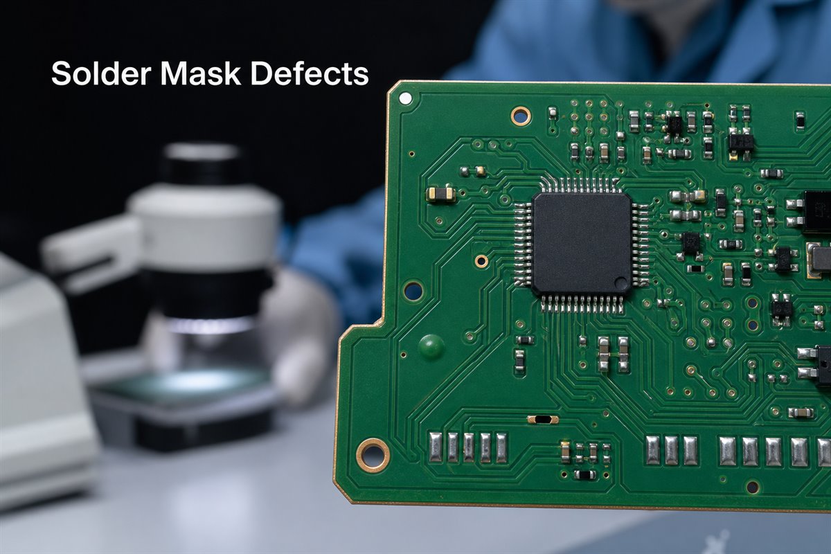
solder mask defects
Inspect solder mask conditions before they become assembly rework.

What Are Solder Mask Defects?

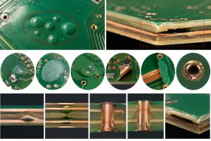
Solder mask defects are unintended problems with PCB mask coverage, openings, alignment, adhesion, curing, or cleanliness. Common signs include exposed copper, mask on pads, pinholes, bubbles, peeling, cracks, contamination, and broken mask dams.

Do not approve a board from appearance alone. Confirm:

  • The affected feature and board location
  • The released Gerber and drawing revision
  • The number of affected boards
  • The applicable acceptance requirement
  • Whether the defect appeared before or after assembly

This gives you a faster, evidence-based disposition instead of a subjective appearance debate.

Common PCB Solder Mask Defects

Match the visible problem with the loss you need to prevent:

What you find What you can prevent
Mask on pads or shifted openings Weak joints and assembly delays
Exposed copper or pinholes Corrosion and reliability escapes
Blisters, peeling, or cracks Heat-triggered failures during PCBA
Broken mask dams Bridging between fine-pitch pads
Via-tenting defects Solder wicking and uneven surfaces
Debris or contamination Adhesion and cleanliness disputes

Location matters more than appearance alone. A small mark on unused laminate is not equal to the same defect on a BGA pad, test point, fine-pitch footprint, or closely spaced conductor.

Ask for a marked defect map and quantity count. You can then see whether the issue is isolated, feature-specific, panel-related, or present across the lot.
solder mask defects
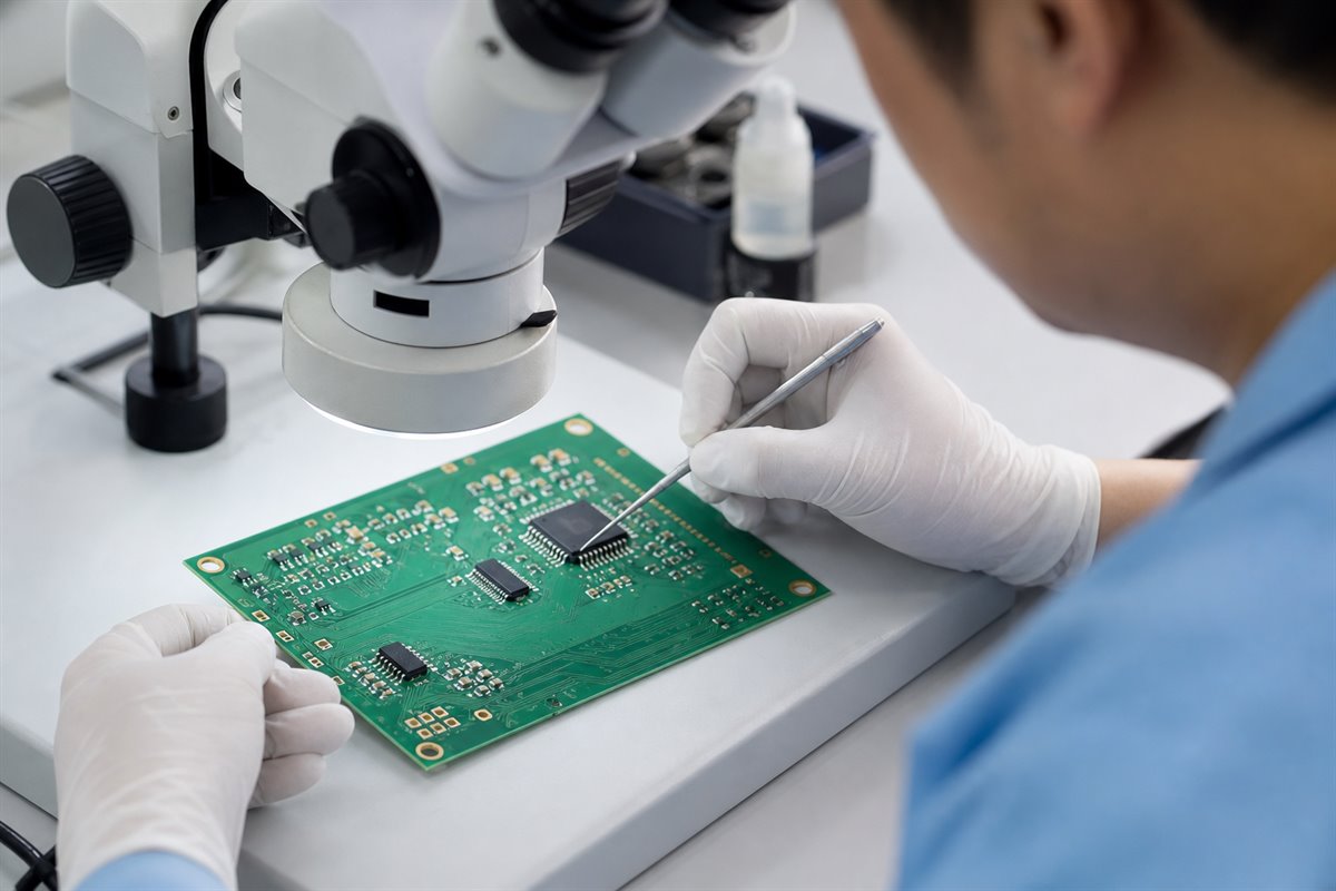
Magnified inspection helps locate mask damage before component placement.

How Solder Mask Problems Affect Assembly and Reliability

Catch solder mask problems before component placement to avoid sorting populated boards later.

Mask on pads can reduce solderable area. Missing dams can increase bridging risk. Weak or undercured mask may blister, crack, or peel during baking, reflow, wave soldering, cleaning, or repair.

Exposed conductors may also lose protection against moisture and contamination. The actual field risk depends on location, spacing, voltage, cleanliness, and the product environment, so appearance alone cannot predict service life.

Early containment helps you avoid:

  • Line stoppage and emergency sorting
  • Weak joints or solder bridges
  • Damage from late-stage rework
  • Shipment delays and repeated lot disputes

Causes of Solder Mask Failure in Design and Fabrication

Separate design, fabrication, and assembly causes before asking for corrective action.

Design data: Incorrect openings, insufficient expansion, unclear via treatment, or mask dams below manufacturing capability can create repeatable defects. Confirm the minimum solder mask sliver the fabricator can hold before releasing fine-pitch data.

Fabrication: Contamination, weak surface preparation, registration error, incorrect processing, or incomplete curing can reduce coverage or adhesion.

Assembly: Excessive heat, incompatible chemistry, fixtures, handling, or repeated rework can damage an otherwise acceptable coating.

Use four checks to reach a decision faster:

Check Decision it supports
Released files and drawing Design issue or fabrication issue?
Defect map and quantity Sort, release, or remake?
Before/after assembly records When did the damage occur?
Material, cure, and process records What must change next lot?

A corrective action should change a file, note, process control, or inspection point. “Pay more attention” does not prevent recurrence.

Simple Tests for Solder Mask Damage

Use agreed tests to obtain release evidence without damaging acceptable boards.

Start with visual inspection under suitable lighting and magnification. Compare the affected area with the same feature on an unaffected board. Record exposed copper, lifted edges, cracked dams, contamination, or color transfer.

Adhesion, hardness, solvent-resistance, or controlled thermal checks may help separate weak adhesion from incomplete curing. When a customer specification calls for IPC-TM-650 testing methods for solder mask, record the exact method number and acceptance limit.

For each test, record:

  • Board revision, lot, sample size, and location
  • Before-and-after photographs
  • Method, conditions, and acceptance limit
  • Results from affected and control samples

Electrical test is not a substitute for mask inspection. A board may pass continuity while still creating soldering or protection risks.

What Inspection Evidence Should a Buyer Request?

Replace “the boards are usable” with evidence that supports your decision.

Request:

  • Close-up photographs with scale and marked locations
  • Lot, panel position, inspected quantity, and defect count
  • Confirmation of the released file and drawing revision
  • The applicable acceptance requirement
  • Test method and actual result
  • Containment status and proposed disposition
  • Root cause and corrective action for repeat defects

For repairs, also approve the material, area, cure method, final thickness, and post-repair inspection. A repair is useful only when it restores protection without reducing pad area or creating a new assembly problem.
solder mask defects
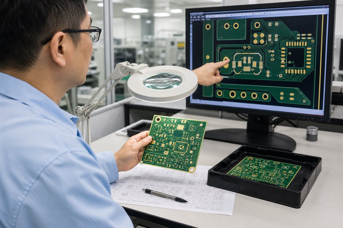
Compare the physical board, released data, and inspection record before disposition.

A Project Example: Reject, Repair, or Release?

Fine-pitch pads show mask encroachment one day before assembly. Releasing the lot risks poor wetting; rejecting every board may create unnecessary delay.

The buyer quarantines the lot and requests a defect map, measurements, file-revision confirmation, and panel-position data. The results show correct Gerber data but a repeatable registration shift in one panel position.

The evidence supports a controlled decision:

  • Release verified unaffected boards
  • Reject or remake boards outside the limit
  • Repair only with customer approval
  • Add a targeted registration check for the next lot

This illustrative example shows the customer benefit: contain first, identify the affected population, and avoid both unsafe release and unnecessary total-lot rejection.

How to Prevent Solder Mask Issues From Repeating

Confirm mask requirements before production so defects do not reach assembly.

Provide synchronized copper, solder mask, drill, and drawing data. State the mask color, finish, via treatment, acceptance standard, and any special thickness or appearance limits.

For dense BGA, fine-pitch, via-in-pad, test-point, and edge-contact areas, request a focused DFM review before releasing the order.

With EBest Circuit (Best Technology), you can confirm solder mask openings, dams, via treatment, and other manufacturability risks before they become assembly rework. You can also coordinate PCB fabrication, PCBA, and agreed inspection evidence with one manufacturing team.

Send previous defect photographs and corrective-action requirements with your RFQ. This directs the review toward the loss you want to prevent. The customer remains responsible for approved design requirements, product-level reliability targets, regulations, and final acceptance.

FAQs About Solder Mask Defects

Can a PCB with solder mask defects still be used? Possibly. Release it only after checking the affected location, quantity, drawing requirement, and assembly risk.

What causes solder mask to peel? Common causes include contamination, poor surface preparation, incomplete curing, heat, incompatible chemistry, or mechanical damage.

Can solder mask over a pad be repaired? Only when the customer approves the method and the repair restores the required solderable area without creating new damage.

Which files help prevent solder mask defects? Provide synchronized Gerbers, drill files, a fabrication drawing, revision notes, via instructions, and acceptance requirements.

What should I send for a solder mask review? Send the approved PCB files, fabrication notes, defect photographs, lot information, and inspection requirements to sales@bestpcbs.com.

You may also like

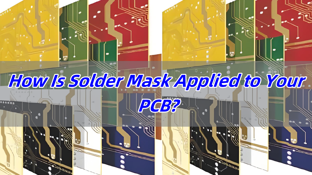
What is Solder Mask in PCB? How Is Solder Mask Applied to Your PCB?
Wednesday, March 26th, 2025

What Is Solder Mask?

A solder mask also called solder resist, it is a protective layer applied to a printed circuit board (PCB) to shield copper traces from oxidation, contamination, and unintended solder bridges. Without this layer, exposed copper can easily corrode or cause short circuits due to accidental solder connections.

Most solder masks are made from epoxy resins, liquid photo imageable (LPI) materials, or dry films. These materials create an insulating layer that only exposes the necessary contact points for soldering, such as component pads. In modern PCB manufacturing, solder masks are essential for ensuring proper functionality, ease of assembly, and long-term reliability. Whether for simple or advanced circuits, a high-quality solder mask is critical for maintaining the integrity of a PCB.

What is Solder Mask in PCB? How Is Solder Mask Applied to Your PCB?

How Is Solder Mask Applied to Your PCB?

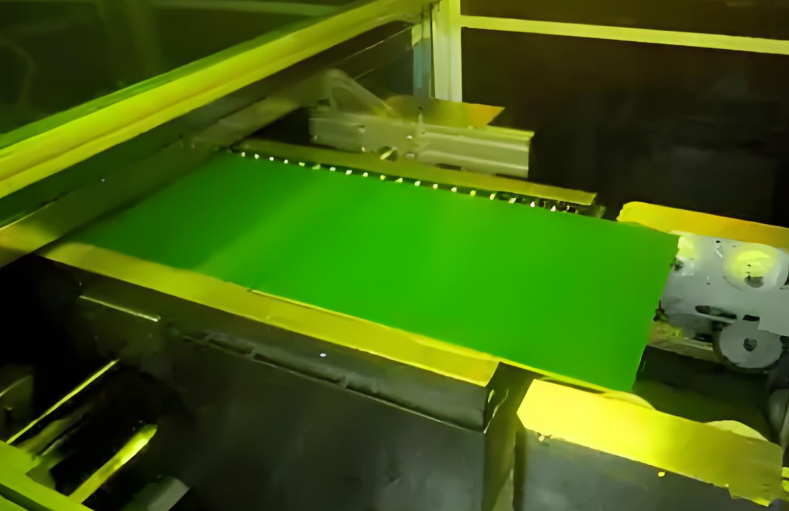
How is solder mask applied to your PCB? Applying a solder mask is a multi-step process that requires precision to ensure even coverage and proper functionality. The process varies depending on the type of solder mask used, but the general steps include:

1. Surface Preparation

Before applying a solder mask, the PCB surface must be thoroughly cleaned. Any dust, grease, or oxidation can affect adhesion. Manufacturers use chemical cleaning or mechanical scrubbing to remove contaminants and prepare the board for coating.

2. Solder Mask Application

The solder mask is applied using one of the following methods:

  •  LPI Solder Mask: A liquid mask is sprayed or screen-printed onto the PCB surface. This method provides excellent precision and is widely used in high-density PCB designs.
  • Dry Film Solder Mask: A pre-cured solder mask film is laminated onto the board and then exposed to UV light for patterning. It is a common method in high-volume manufacturing.
  • Epoxy-Based Solder Mask: A thermosetting polymer is screen-printed onto the board and then cured. This is one of the oldest methods but is less precise than LPI.
What is Solder Mask in PCB? How Is Solder Mask Applied to Your PCB?

3. UV Exposure and Developing

After application, the board is exposed to ultraviolet (UV) light through a photomask that defines the solder mask openings. The exposed areas harden, while the unexposed parts remain soft and can be removed using a developer solution.

4. Curing and Final Inspection

Once the mask is developed, the PCB undergoes a curing process, usually in an oven, to fully harden the solder mask. Afterward, the board is inspected to ensure the mask is properly applied without defects. Evenly application of the solder mask is essential for preventing soldering issues and ensuring the long-term reliability of the PCB.

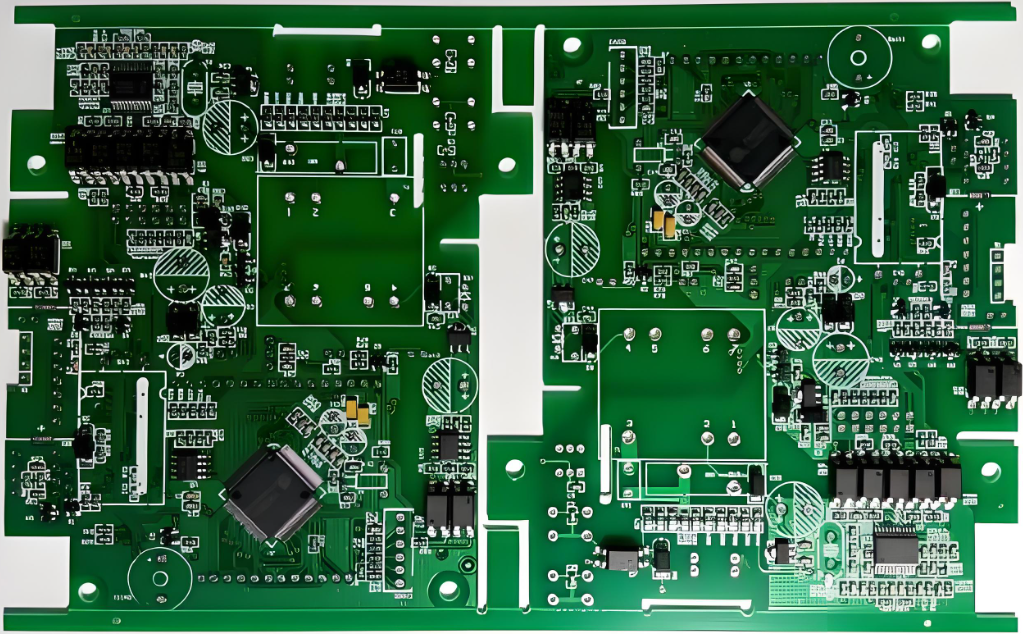
Why Is the Solder Mask Green?

The green color of solder masks became the industry standard due to a combination of historical, practical, and technical factors. Early PCB manufacturing processes used epoxy-based resins, which naturally had a green tint. Over time, manufacturers standardized this color because it offered excellent contrast for visual inspection. Engineers and technicians rely on automated optical inspection (AOI) systems to detect defects, and the green color provides the best balance between visibility and eye strain. Other colors like red, blue, and black exist, but green remains the most widely used due to its well-established reliability and cost-effectiveness.

What is Solder Mask in PCB? How Is Solder Mask Applied to Your PCB?

Beyond visibility, green solder masks also offer superior thermal and chemical stability compared to some other colors. PCBs endure high temperatures during soldering, and green formulations have been extensively tested to withstand heat without degrading.

What Can I Use Instead of a Solder Mask Material?

If a solder mask isn’t available, there are alternative methods to protect PCB copper traces. However, they may not provide the same level of durability and precision.

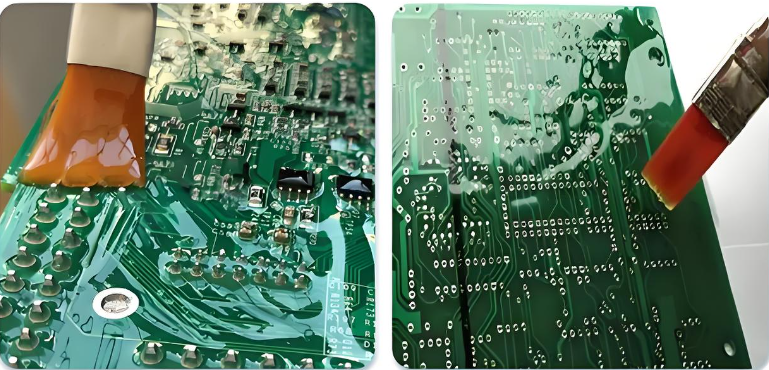
1. Conformal Coatings

Conformal coatings are thin protective layers applied to PCBs to protect against moisture, dust, and corrosion. While they don’t replace solder masks, they can provide an extra layer of protection. Some PCBAs may required to coating a layer of conformal as an extra protect layer.

What is Solder Mask in PCB? How Is Solder Mask Applied to Your PCB?

2. Kapton Tape

Kapton tape is a heat-resistant, electrically insulating material that can be used to protect specific areas of a PCB. However, it doesn’t offer the same level of coverage or durability as a solder mask.

3. PCB Lacquers

Some manufacturers use specialized PCB lacquers to coat copper traces and prevent oxidation. These coatings are easy to apply but may wear off over time.

4. DIY Solutions

Some electronics hobbyists use clear nail polish as a temporary solder mask substitute. While it can offer short-term protection, it is not a recommended solution for professional PCBs.

A proper solder mask is always the best choice for ensuring the longevity and reliability of a PCB.

How Do You Apply Solder Mask Evenly?

A smooth and uniform solder mask application is crucial for avoiding defects. Here are some key factors to consider:

1. Clean the PCB Surface: Any dust or grease can cause uneven adhesion. Proper cleaning ensures the mask spreads evenly.

2. Use Controlled Application Methods: Automated spraying, screen printing, or laminating techniques help distribute the solder mask uniformly.

3. Maintain Proper Viscosity: If the solder mask is too thick or too thin, it may not spread evenly. Maintaining the right consistency ensures better coverage.

4. Ensure Proper Curing: Over-curing or under-curing can create issues with adhesion and durability. Controlled UV exposure and thermal curing help achieve the best results.

What Is the Solder Mask Requirement?

Solder mask requirements vary depending on PCB design, industry standards, and application needs. The mask must very good to protect the board from oxidation, solder bridges, and contaminants. Manufacturers should follow strict guidelines to ensure the solder mask meets performance and quality expectations. And customers also can inspect these parameters to make sure solder mask is good.

1. Thickness Requirements

The solder mask must maintain a consistent thickness to prevent defects. Typical thickness values are:

  • Over Copper Traces: 15–35 ÎŒm (micrometers)
  • Over Substrate (Bare Board Areas): 5–15 ÎŒm
  • Near SMD Pads and Through-Holes: Sufficient clearance to avoid interference with soldering.

An uneven or excessively thick mask can cause soldering issues, while a thin mask may not provide enough protection.

What is Solder Mask in PCB? How Is Solder Mask Applied to Your PCB?

2. Registration Accuracy

The solder mask must align precisely with the PCB layout. Misalignment can lead to:

  • Blocked SMD pads or vias, affecting solderability.
  • Unprotected traces, increasing the risk of oxidation or short circuits.

Industry standards, such as IPC-6012, define the allowable misregistration, typically within ±3 mils (±0.075 mm) to ensure proper coverage.

3. Clearance and Openings

The solder mask must be designed with appropriate clearances around pads and vias to ensure smooth soldering. Key points include:

  • Pad-to-solder mask clearance: Typically 3–5 mils (0.075–0.125 mm) to prevent solder mask from covering pad edges.
  • Via coverage: Some designs require tenting (fully covering the via), while others leave vias exposed for better connectivity.

4. Electrical Insulation Properties

Solder masks act as an insulating layer to prevent short circuits between copper traces. The dielectric strength must be high enough to withstand PCB operating voltages. Common requirements include:

  • Dielectric strength: Above 500V/mil for proper insulation.
  • Surface resistivity: Greater than 10âč Ω/sq to prevent leakage currents.

5. Compliance with Industry Standards

Solder mask materials and application processes must comply with international standards, such as: IPC-SM-840, RoHS & REACH, UL 94V-0.

What Kinds of Solder Masks Do We Have in EBest Circuit (Best Technology)?

At EBest Circuit (Best Technology), we offer a range of solder masks to suit different PCB applications. Our selection includes:

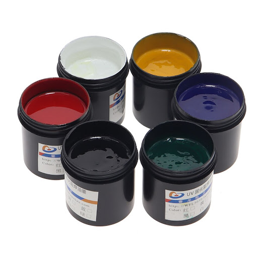
  • Green (commonly select)
  • Red (for prototype)
  • Blue (for power supply board)
  • Black (consumer electronics)
  • Matte Black (high-end products or prototypes)
  • White (lightings)
  • Grey (prototypes)
  • Matte Grey (prototypes)
  • Yellow (rarely used)
  • Purple (prototype or high-end product that need good appearance)

We ensure that our solder masks meet industry standards, providing excellent adhesion, thermal stability, and long-term reliability. Would you like to discuss a specific solder mask for your PCB project? Contact us today!

You may also like

What is the solder mask? PCB basic information
Wednesday, February 19th, 2025

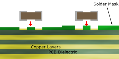
What is a solder mask? The solder mask on the PCB is a special coating covering the surface of the circuit board, usually composed of polymer resins, pigments and other materials. It is used to prevent solder from flowing into non-soldering areas during soldering, avoid short circuits, and protect copper lines from oxidation and environmental erosion.

What is the solder mask on a PCB?

What is solder mask layer on pcb?

The solder mask layer is a thin polymer layer applied to the surface of a PCB to protect the copper traces from exposure to air, moisture, and solder during assembly. It is typically applied as a liquid and then cured to create a durable, insulating coating.

This layer ensures that solder only adheres to designated areas, such as component pads, while preventing unintentional connections that can cause electrical failures.

Most PCBs feature a solder mask on both sides, covering all traces except for the exposed pads where components will be soldered. The mask enhances the board’s mechanical strength, providing extra durability against physical damage.

What is a solder mask used for?

A solder mask serves multiple functions in PCB manufacturing and assembly, including:

What is the solder mask on a PCB?
  • Prevents Solder Bridging – Stops accidental solder connections between closely spaced components.
  • Protects Copper Traces – Shields against oxidation and environmental damage.
  • Improves Electrical Insulation – Reduces the risk of unintended electrical contact between conductive traces.
  • Enhances PCB Durability – Adds a layer of mechanical strength, preventing wear and tear.
  • Aesthetic Enhancement – Gives PCBs a smooth, uniform finish and a professional appearance.

By preventing shorts and increasing reliability, the solder mask plays an essential role in producing high-performance circuit boards.

What is the standard thickness of a solder mask layer?

The thickness of a solder mask depends on the manufacturing method and the type of PCB. The most common solder mask thickness values are:

  • Liquid Photoimageable (LPI) Solder Mask: 0.7 to 1.5 mils (18-38 microns)
  • Dry Film Solder Mask: 0.5 to 1.2 mils (12-30 microns)
  • UV Curable Solder Mask: 0.2 to 1.0 mils (5-25 microns)

A well-applied solder mask ensures proper adhesion and durability without interfering with PCB functionality.

How to apply solder mask to a pcb?

The solder mask application process follows precise steps to ensure uniform coverage and proper curing:

What is the solder mask on a PCB?
  • Surface Preparation – The PCB is cleaned to remove dust, oils, and oxidation.
  • Curtain Coating – Ideal for high-volume production.
  • Spray Coating – Suitable for complex multilayer boards.
  • Pre-baking – The board is partially cured to enhance adhesion.
  • UV Exposure – The solder mask is exposed to UV light through a photomask to define areas where it should remain.
  • Development & Cleaning – Uncured mask material is removed to reveal solder pads.
  • Final Curing – The PCB undergoes heat curing for maximum durability.

This process ensures a strong, long-lasting solder mask layer that can withstand harsh conditions.

How long does it take for solder mask to cure?

Curing time depends on the method used:

  • UV Curing: A few minutes with high-intensity UV exposure.
  • Thermal Curing: 30-60 minutes at 150°C (302°F) for enhanced durability.
  • Combination Curing: UV exposure followed by thermal curing for optimal strength.

Proper curing is crucial to prevent defects like delamination, peeling, or cracking.

Does solder mask color matter?

The color of a solder mask does not affect PCB performance, but it can impact visibility, aesthetics, and inspection efficiency. Common colors include:

What is the solder mask on a PCB?
  • Green – The industry standard for optimal contrast and easy inspection.
  • Blue – Provides high contrast with white silkscreen text.
  • Red – Used for high-end or custom branding.
  • Black – Reduces light reflection but makes defect detection harder.

While color selection is mostly aesthetic, certain colors may aid in automated optical inspection (AOI) processes.

Why is most solder mask green?

Green solder mask is widely used due to:

  • Best Visibility for AOI – The contrast makes defect detection easier.
  • Industry Standardization – Manufacturers are optimized for green solder mask production.
  • High Durability – Green solder masks tend to have better adhesion and chemical resistance.

However, manufacturers can produce PCBs with different solder mask colors based on specific project needs.

What is the difference between blue and green solder masks?

The key differences between blue and green solder masks are:

  • Green – Best for automated inspection, high contrast, and industry standard.
  • Blue – Vibrant appearance but slightly harder for AOI systems to detect defects.

Both options provide reliable protection, and the choice depends on aesthetic and inspection needs.

What is the difference between solder mask and solder paste?

Solder mask and solder paste serve different purposes in PCB assembly:

  • Solder Mask – A permanent protective coating that prevents unintended soldering and oxidation.
  • Solder Paste – A temporary material containing metal particles and flux, used to attach components before reflow soldering.

Both are essential for high-quality PCB production, but they are applied at different stages.

Conclusion:

In summary, the solder mask plays a critical role in ensuring the longevity and reliability of a PCB. It protects the copper traces, prevents soldering errors, and improves overall circuit board performance.

At EBest Circuit (Best Technology), we are committed to delivering high-quality PCBs, with precise solder mask application, to meet your specific needs. Contact us today for customized PCB solutions that will elevate your product’s performance. Email: sales@bestpcbs.com

You may also like