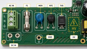
A PCB interposer is an intermediate printed circuit board that remaps pads, pins, power rails, or signals between two incompatible interfaces. Typical uses include adapting a new BGA to a legacy footprint, expanding a fine-pitch device into a testable array, and connecting boards or sockets with different pin assignments. Its design must control the complete transition from the first pad field through vias and routing to the second interface.

Do You Need an Organic PCB Interposer or a Package-Level Interposer?
Choose the supplier from the interconnect level, not from the word interposer. An organic PCB interposer is fabricated with laminate, copper circuitry, plated holes or microvias, solder mask, and a board-level surface finish. A silicon interposer uses semiconductor processes and may contain through-silicon vias. Glass and advanced package substrates also require different fabrication equipment and qualification methods.
| Structure | Connection Level | Typical Fabrication Route | Primary Design Constraint |
| Organic PCB interposer | Package-to-board, board-to-board, socket, or test interface | Multilayer PCB or HDI processes | BGA escape, via geometry, planarity, impedance, and assembly |
| IC package substrate | Die or package to system board | Fine-line organic substrate processes | Package warpage, fine pitch, and substrate reliability |
| Silicon interposer | Die-to-die or die-to-package in 2.5D integration | Semiconductor lithography, often with TSVs | Microbump density, TSV design, and thermal stress |
| Glass interposer | Advanced package redistribution | Specialized glass-via and metallization processes | Via formation, metallization adhesion, and handling |
If the input data contains bare-die bumps, microbumps, TSVs, redistribution layers, or package-level warpage requirements, route the project to an advanced-packaging supplier. If both sides are conventional pads, BGA lands, connectors, sockets, or test contacts that can be built with PCB processes, continue with an organic PCB feasibility review.
Which Inputs Must Be Fixed Before Stackup Design?
Freeze both mating interfaces and their electrical mapping before selecting layer count or via type. The design team needs controlled coordinates, orientation, pin names, mechanical datums, installed height, attachment method, and service conditions for both sides. A mirrored footprint or outdated pin map can produce a board that passes fabrication inspection but connects the wrong nets.
- Interface geometry: provide pad coordinates, package drawings, body outline, keepouts, datum locations, connector or socket drawings, and allowable positional error.
- Pin mapping: identify every signal, ground, power, no-connect, reserved pin, polarity mark, and remapped connection in a controlled table.
- Electrical limits: state impedance, current, voltage spacing, differential-pair skew, insertion-loss budget, and any sensitive analog or clock nets.
- Assembly route: define soldered, socketed, compression-contact, or test-only use; also state which side is assembled first and the number of thermal cycles.
- Mechanical limits: specify total thickness, flatness or coplanarity, component clearance, support points, contact force, and allowable board deflection.
- Service profile: include operating and storage temperature, vibration, expected mating cycles, moisture exposure, cleanliness, and target life.
How Should the BGA Escape and Stackup Be Built?
Derive the stackup from routing channels, reference-plane continuity, and manufacturable via transitions. Start by grouping pins into ground, power, high-speed, low-speed, analog, clock, and unused classes. Then estimate how many traces must leave each BGA ring and which layer changes are unavoidable.

- Route the outer rows: use surface escape where trace width, clearance, and solder-mask geometry provide adequate manufacturing margin.
- Assign via structures: use through holes when pitch permits; introduce blind microvias or via-in-pad only where inner rows cannot escape otherwise.
- Reserve reference planes: keep controlled-impedance signals adjacent to continuous ground and provide nearby ground transitions at every signal-layer change.
- Distribute power: size copper and via arrays from current and transient requirements, then place decoupling where the connection inductance remains useful.
- Check lamination sequence: map each blind and buried via to a real build stage; stacked microvias and multiple sequential laminations require an explicit reliability review.
- Balance copper: correct large density differences between the central pad field and the perimeter to reduce bow, twist, and registration variation.
Via-in-pad must be called out as filled, capped, and planarized when the pad will be soldered. Leaving the construction undefined can cause solder loss into the via, insufficient joint volume, and uneven pad surfaces. Backdrilling may reduce through-via stubs, but it requires adequate stub access, drill tolerance, and clearance from adjacent structures.
Which Parameters Control Signal and Power Integrity?
Analyze the pad, via, trace, plane reference, and mating joint as one electrical discontinuity. Short interposers can still degrade fast interfaces because their transitions may contain large pads, long via stubs, anti-pad changes, or interrupted return paths.
- Impedance: calculate from the proposed production stackup, including finished copper, dielectric thickness, resin content, trace geometry, and fabrication tolerance.
- Return path: prevent plane splits and voids below fast routes; place ground vias close to signal vias when the route changes layers.
- Via discontinuity: evaluate barrel length, unused stub, pad diameter, anti-pad diameter, and nearby ground-via placement.
- Differential symmetry: match the two paths through pads and vias, not only along straight traces; control intra-pair skew at the transition.
- Crosstalk: evaluate spacing together with parallel length, edge rate, reference distance, and allowable coupled noise; a fixed spacing ratio is not a universal acceptance rule.
- Power impedance: minimize loop inductance through paired power-ground vias, suitable plane spacing, and decoupling connected with short, wide paths.
Use impedance coupons for fabrication control, TDR for time-domain discontinuity location, and S-parameters or an end-to-end link test when insertion loss, return loss, or crosstalk is part of the interface budget. Match the test method and frequency range to the actual signal instead of using a generic high-speed label.
What Manufacturing Limits Require an Early DFM Review?
No single minimum-feature value proves that a dense interposer is manufacturable. Pad pitch must accommodate trace escape, capture pads, anti-pads, solder-mask openings, registration allowance, copper thickness, via fill, and the selected lamination sequence at the same time.
| Capability Item | General Capability | Special Process or Review |
| FR-4 layer count | 1-10 layers; high-Tg material noted for 8 layers and above | 10-32 layers |
| Laser blind or buried via diameter | 0.10 mm | Project-specific stackup review |
| Minimum finished mechanical hole | 0.20 mm | 0.15 mm |
| Through-hole aspect ratio | 8:1 | 10:1 |
| Inner-layer line/space at 0.5 or 1 oz | 4/4 mil | 3/3 mil |
| Outer-layer line/space at 1 oz | 4/4 mil | 3/3 mil |
| Solder-mask opening, single side | 2 mil | 1 mil |
| ENIG thickness | Gold 0.025-0.125 micrometers; nickel 3-8 micrometers | Confirm against pad function and assembly criteria |
These values come from the current general PCB capability workbook and are feasibility boundaries, not automatic design rules. EBest Circuit must review the actual BGA map, copper weight, material, panel construction, via sequence, solder-mask strategy, and acceptance criteria before confirming a special-process design.
How Is an Organic PCB Interposer Manufactured?
Organic PCB production is the base process. Dense pad fields add tighter controls for registration, via filling, planarity, and copper balance.
- Verify data: compare the netlist, layer stack, drill pairs, pin map, dimensions, impedance notes, and finish requirements before tooling.
- Form inner layers: image and etch copper, then inspect line width, spacing, annular rings, and defects before lamination.
- Laminate the structure: control resin flow, dielectric thickness, copper distribution, and layer registration across each build cycle.
- Create interconnects: drill mechanical holes or laser microvias, desmear, metallize, and plate to the specified layer pairs.
- Fill via-in-pad: fill, cure, planarize, and cap solderable pads so that the assembly surface remains flat and sealed.
- Form outer layers: image and etch the final circuitry, then inspect critical pads, traces, and clearances.
- Apply mask and finish: control solder-mask registration and apply the approved surface finish for soldering or contact use.
- Profile and test: route the outline, inspect dimensions, perform electrical test, and complete the defined coupon or microsection checks.
Which Failure Modes Should the Design and Test Plan Control?
Each critical failure needs a defined prevention method and a measurable detection method. Continuity testing alone cannot detect planarity, joint fatigue, impedance discontinuities, or weak microvias.
| Failure Mode | Primary Cause | Design Control | Verification |
| Wrong net connection | Mirrored footprint, orientation error, or uncontrolled pin-map revision | Independent coordinate and netlist comparison | Electrical test against the approved netlist |
| Solder wicking | Open or incompletely filled via-in-pad | Filled, capped, and planarized construction | Cross-section and assembly inspection |
| Open or intermittent joint | Warpage, contamination, inadequate solder volume, or unstable contact force | Flatness, finish, stencil or socket, and support controls | X-ray, coplanarity measurement, and continuity under load |
| Signal reflection | Via stub, pad/anti-pad discontinuity, or reference-plane interruption | Transition modeling and controlled return path | TDR, S-parameters, or link test |
| Microvia fatigue | Stacked geometry, high thermal stress, or unsuitable lamination sequence | Via-structure and stackup reliability review | Thermal cycling with resistance monitoring and cross-section |
| Pad or laminate damage | Board bending, socket force, shock, or poor support | Mechanical load-path and thickness review | Strain measurement, mechanical test, or destructive analysis |
How Should the Finished PCB Interposer Be Validated?
Validate in four stages: data correctness, bare-board quality, assembled-interface quality, and application performance.
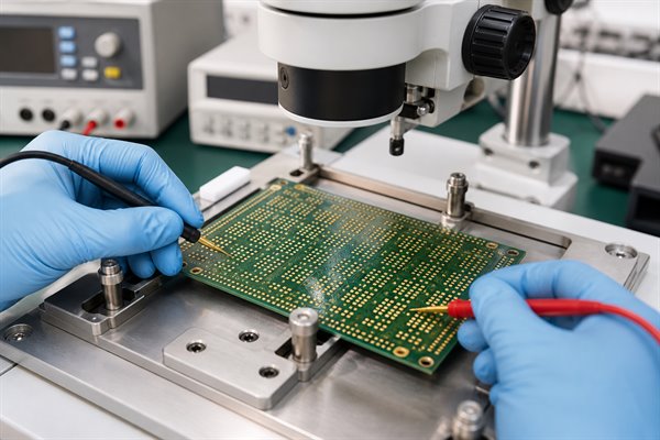
- Data comparison: verify fabrication data, drill pairs, stackup, netlist, and pin-map revision before production release.
- Dimensional inspection: measure thickness, outline, datum locations, hole and pad positions, and bow or twist where mating alignment depends on them.
- Electrical test: check opens and shorts; add four-wire resistance limits for low-resistance power or measurement paths when required.
- Microsection: inspect plating, via fill, registration, dielectric condition, and interconnect structure on representative coupons or boards.
- Assembly inspection: evaluate hidden solder joints by X-ray and inspect bridging, voiding, solder volume, wetting, and alignment against defined limits.
- Signal verification: use impedance coupons, TDR, S-parameters, or a functional link test according to the electrical risk.
- Reliability verification: select thermal cycling, vibration, mechanical loading, or mating-cycle testing from the actual service profile.
The purchase specification must name the test, sampling level, equipment or method, numerical acceptance limit, and disposition for failure. “100% electrical test” is meaningful only when the controlled netlist and tested characteristics are identified.
What Determines PCB Interposer Cost and Supplier Suitability?
PCB interposer cost is driven by the number of special operations and the manufacturing margin left around critical features. A small board can still be expensive when it requires sequential lamination, stacked or filled microvias, fine line/space, tight registration, controlled flatness, impedance coupons, or extensive inspection. Quantity and panel utilization matter, but they do not remove the cost of a complex build sequence.
| Cost Driver | Why It Changes the Quote | RFQ Action |
| Layer and lamination structure | Additional build cycles increase processing, registration control, inspection, and failure exposure. | Request the proposed stackup and a layer-pair diagram for every blind or buried via. |
| Microvia and via-in-pad construction | Laser drilling, filling, planarization, copper capping, and stacked structures add controlled operations. | Identify which pads require filled and capped vias; do not apply the requirement to every via by default. |
| Fine features and tolerances | Line/space, annular ring, solder-mask registration, positional accuracy, thickness, and flatness interact and can reduce yield margin. | Mark each tolerance as functional, preferred, or open to supplier proposal. |
| Material and surface finish | Material availability, stackup thickness, copper weight, finish type, and finish thickness affect sourcing and process compatibility. | State the required electrical, thermal, soldering, or contact function instead of naming an unsupported substitute. |
| Electrical control | Controlled impedance, low-resistance paths, and high-frequency limits require stackup calculations, coupons, or additional measurements. | List the controlled nets, target values, tolerances, test method, and required report. |
| Inspection and reliability evidence | Dimensional reports, microsections, X-ray, TDR, S-parameters, thermal cycling, and traceability add work only when specified as deliverables. | Separate mandatory production acceptance from qualification or optional engineering tests. |
| Assembly responsibility | Bare-board supply, solder-ball attachment, component assembly, socket integration, and functional testing have different tooling and quality ownership. | Define the delivery state and assign responsibility for each mating interface. |
Compare quotations only after normalizing their scope. One supplier may include via filling, impedance coupons, electrical test, dimensional reporting, and assembly inspection, while another may quote only the bare board. Ask each supplier to identify exclusions, special-process charges, tooling, test coverage, supplied reports, and the design changes assumed in the price.
A technically suitable supplier should return a manufacturable stackup, a complete via sequence, the features that consume the smallest process margin, and any proposed changes to pads, anti-pads, mask openings, copper balance, or tolerances. The response should also identify which operations are performed and controlled within its qualified supply chain. Silicon, glass, and bare-die package structures require an advanced-packaging route and should not be evaluated as conventional PCB work.
What Should Be Included in the Engineering Review Package?
The review package must reproduce both interfaces without assumptions. It must also control their mapping, board construction, and acceptance criteria.
- Fabrication package: Gerber X2 or ODB++, NC drill files with layer pairs, IPC-356 or equivalent netlist, fabrication drawing, outline, and stackup.
- Interface package: land-pattern coordinates, package and connector drawings, pin maps, orientation, datums, keepouts, and height limits.
- Electrical package: net classes, impedance and skew limits, current by rail, voltage spacing, loss budget, and required measurements.
- Material package: laminate performance requirements, copper weight, solder mask, surface finish, and restricted-substance requirements.
- Assembly package: BOM where applicable, centroid data, paste intent, reflow limits, inspection criteria, and handling controls.
- Quality package: acceptance class or customer specification, sampling, coupon plan, dimensional report, microsection criteria, traceability, and reliability tests.
Mark every requirement as mandatory, preferred, or open to supplier proposal. This prevents inherited layout habits from being treated as fixed system requirements and makes DFM changes auditable.
FAQs About PCB Interposer
Q1: Can one PCB interposer support several package variants?
A1: Only when the pad geometry and pin mapping remain unambiguous. Shared pads, jumpers, or option components must not create unterminated stubs, accidental shorts, or an assembly configuration that cannot be inspected.
Q2: When is a socketed interposer preferable to a soldered one?
A2: Use a socket when replacement, repeated testing, or device preservation is more important than minimum height and transition loss. Confirm contact resistance, force, wear, alignment, and bandwidth.
Q3: Does a thicker interposer improve reliability?
A3: Not automatically. Greater thickness can increase stiffness but also lengthen vias and change solder-joint or socket loading; evaluate electrical and mechanical effects together.
Q4: Can ENIG be used for every interposer contact?
A4: ENIG is common for solderable pads, but the contact function determines the finish. Repeated mechanical contacts, wire bonding, fine-pitch assembly, or special storage requirements may require another finish and separate confirmation.
Q5: When is backdrilling worth adding?
A5: Add backdrilling when the unused through-via stub consumes a meaningful part of the channel budget. Confirm remaining stub, drill tolerance, accessible side, and nearby-clearance limits before release.
Q6: Should unused BGA pads be removed?
A6: Remove or retain them only after checking routing space, assembly balance, inspection needs, and future variants. Unused pads must not be mistaken for connected or testable nodes.
Q7: How should orientation be controlled?
A7: Use at least two independent controls. Combine pin-one marking with asymmetric datums, keyed mechanical features, coordinate tables, or an assembly drawing that cannot be mirrored.
Q8: Is a functional test enough for production acceptance?
A8: Functional testing does not replace bare-board netlist testing or structural inspection. It may miss latent microvia, plating, dimensional, and process defects that have not yet caused system failure.
Q9: When should a test coupon be added?
A9: Add a coupon when production verification requires a representative structure that cannot be measured reliably on the finished board. Examples include impedance, plating, microvia, and lamination checks.
Q10: What must be controlled when the interposer is reworked?
A10: Limit cumulative heat, pad damage, laminate moisture, and mechanical bending. Define the permitted rework cycle, thermal profile, cleaning method, inspection, and acceptance test before reusing the assembly.
Conclusion
A reliable PCB interposer begins with controlled interface data and ends with measurable acceptance evidence. Freeze both pad fields and the pin map, derive the stackup from escape and reference requirements, review every via against the real build sequence, and connect each failure risk to a defined inspection or test.
For an organic PCB interposer review, send the fabrication data, pin maps, stackup, impedance targets, assembly method, service profile, and acceptance criteria to sales@bestpcbs.com. EBest Circuit will review the printed-board construction and identify features that require special-process confirmation.